Leveraging Plasmonic Hot Electrons to Quench Defect Emission in Metal - Semiconductor Nanostructured Hybrids: Experiment and Modeling
Abstract
Modeling light-matter interaction in hybrid plasmonic materials is vital to their widening relevance from optoelectronics to photocatalysis. Here, we explore photoluminescence from ZnO nanorods (ZNR) embedded with gold nanoparticles (Au NPs). Progressive increase in Au NP concentration introduces significant structural disorder and defects in the ZNRs, which paradoxically quenches defect related visible photoluminescence (PL) while intensifying the near band edge (NBE) emission. Under UV excitation, the simulated semi-classical model realizes PL from ZnO with sub-band gap defect states, eliciting visible emissions that are absorbed by Au NPs to generate a non-equilibrium hot carrier distribution. The photo-stimulated hot carriers, transferred to ZnO, substantially modify its steady-state luminescence, reducing NBE emission lifetime and altering the abundance of ionized defect states, finally reducing visible emission. The simulations show that the change in the interfacial band bending at the Au-ZnO interface under optical illumination facilitates charge transfer between the components. This work provides a general foundation to observe and model the hot carrier dynamics in hybrid plasmonic systems.
I Introduction
Surface plasmon resonances (SPR) of metal nanostructures finds wide-ranging applications stemming from the capability to concentrate and enhance light energy into ultra-small sub-wavelength volumes and their large scattering cross-section in the visible [1, 2, 3, 4, 5, 6, 7]. The localized surface plasmons (LSP) and the polaritons de-excite radiatively [8, 9] or, more often non-radiatively through electron-electron, electron-phonon and defect or surface scattering [10, 11, 12], which has been exploited for localized heating[13]. Plasmons may also decay via secondary electron-hole (e-h) pair generation, forming an uncorrelated, non-equilibrium hot carrier distribution. The distribution is commensurate with the plasmon energy () and characterized by a temperature () that is significantly higher than the equilibrium lattice temperature () [14]. There is significant interest in exploiting hot carrier dynamics in an emerging class of hybrid plasmonic systems composed of plasmonic nanostructures and semiconductors. The emission properties of semiconducting emitters often benefit from overlap in its spectral response with plasmonic field enhancement[15]. However, even in the off-resonant regime, hybrid systems can be designed to leverage hot carriers to tailor the spectral characteristics and improve efficiency of photovoltaic devices and photocatalysts[16, 17, 18, 19].
Here, we explore a hybrid plasmonic system of ZnO nanorods (ZNR) embedded with Au nanoparticles (NP). ZnO, a wide band gap ( 3.3 eV) semiconductor, has been widely explored in conjunction with plasmonic NPs to achieve luminescence tuning, enhanced sensor performance[20, 21, 22], and improved photocatalytic activity [23, 24, 25]. The typical photoluminescence (PL) spectrum of ZnO shows a distinct near band edge (NBE) excitonic peak around 370 nm, along with broad emission in the visible, that is attributed to interstitial Zn () and deep level (DL) oxygen vacancy () related defects[26]. Consequently, the intensity and spectral composition of visible emission is highly dependent on the growth conditions and morphology of the nanostructures and are susceptible to environmental conditions [27]. The PL is also influenced by the highly inhomogeneous distribution of the neutral and ionized defect states (), especially at interfaces and grain boundaries [28]. Previous investigations from our group [29] and others [30, 31, 32, 33, 34, 35, 36, 37] have shown that ZnO nanostructures coupled with plasmonic NPs lead to decay in visible PL, simultaneously enhancing NBE emission, a similar observation has been reported in Ag-GaN hybrids [38] which have been exploited for novel applications in photovoltaics and spectroscopy[39]. While the reports recognize strong coupling between the components that enable charge & energy transfer, the investigations do not elucidate the role of the Au-ZnO Schottky interface, especially under photoexcitation that influences carrier exchange[40]. Reduction of barrier width comparable to hot electron mean free path in the NPs [41, 42] and embedding NPs within the semiconductor have been shown to increase charge transport efficiency[43], highlighting the importance of not only the choice of materials but also the geometry of inclusion. Effective engineering of hybrid systems and exploitation of their novelties also requires comprehension of the multiple concurrent physical processes that enrich the response of such hybrids. Previous theoretical investigations have modeled PL in wide band gap systems and their variation with experimental control parameters, both in the steady state[44, 45, 46, 47] as well as their temporal response[48]. Further, the proximity effect of plasmonic NPs on semiconductor emitters, modifying their decay rates have been variously modeled to elucidate the role of emitter-plasmon coupling [49]. However, these investigations omit the concurrence of several energetic and dynamical processes that plasmonic nanostructures induce in hybrid systems, finally modifying the emission properties of the semiconductor. Our investigation is also motivated by a paucity of models with well-delineated parameters that simulate optical processes in the constituent materials and further offer physically motivated coupling that determines and controls the PL of the hybrid system.

Here, Au NPs embedded in the ZnO matrix create the most intimate and pristine contact between the two materials and modify the PL spectrum as shown in Fig.1. PL spectra of bare ZNR samples prepared under identical conditions show wide variation, especially in visible emission. Spectra from samples with increasing Au NP inclusion lead to progressive quenching of visible emission, accompanied by NBE emission enhancement. The results are counter intuitive since the ZNRs become morphologically disordered with increasing NP incorporation, nucleating increasing density of native defects that would aid visible emission. We present a combined experimental and theoretical study to explore the spectral response of this hybrid plasmonic system with increasing Au NP inclusion in ZnO. Finite element method (FEM) modeling is used to implement a semiclassical calculation to obtain recombination rates for bare ZNRs that are later augmented by modeling energy and charge transfer processes arising due to Au NP inclusion. Under UV illumination, the model evinces change to the metal-semiconductor interfacial band alignment which, along with an estimate for hot carrier density generated in the NPs, quantifies electron transfer from Au to ZnO. The results show direct increase in the interband transition rate and also reveal increased electron occupancy of the DL ionized defect states in ZnO, due to electron transfer. This indirect occupancy modulation leads to the observed quenching in visible emission. Diverse applicability of hybrid plasmonic systems contextualizes the relevance of the present exercise in modeling their optical properties that may be extended to provide insights into the properties and parameters which govern their response.
II Experimental and Model details
All chemicals, including zinc nitrate hexahydrate, hexamethylene-tetramine (HMTA), Au NPs of mean diameter 30 () nm, were supplied by Sigma Aldrich. All ZNR samples were grown by a low-temperature hydrothermal route[26] on Zn foil substrate, as detailed in Supplemental Material (SM) Section S1. A process with slow ZNR growth kinetics was chosen to promote the incorporation and retention of Au NPs within the ZnO lattice. To embed AuNP within the ZNR, a suspension of AuNPs in a stabilizing buffer ( particles/ml) was added to the growth solution. SM table S1 lists the Au:Zn atomic ratio in the growth solution. By simultaneously increasing the AuNP solution volume and decreasing the zinc nitrate hexahydrate+HMTA stock solution volume, we obtain samples ranging from least AuNP inclusion(bare ZNR) to maximum inclusion(5AZn).
Morphological characterization was performed using a field-emission scanning electron microscope (SEM, Nova Nano SEM 450) and transmission electron microscope (TEM, TECHNAI G2-TF-30). Structural analysis was carried out using a powder x-ray diffractometer (Empyrean, PANalytical) with reference radiation of Cu Kα = 1.540 Å. X-ray photo-electron spectroscopy (XPS) was done using a Scienta Omicron XPS system. The Raman spectra were recorded with 638 nm and 532 nm excitation (Horiba Scientific Xplora Plus). PL spectra were recorded using a custom made setup using a spectrometer (Shamrock 303i and iDus 420 CCD, Oxford Instruments) under 320 nm laser excitation. All numerical calculations were performed using codes developed in Mathematica, python and finite element method (FEM) calculation software COMSOL Multiphysics 5.3a. Details of the model parameters are available in the SM Sections S3, S4 and S5. The optical properties of Au used are given by Rakic et al. [50]. ZnO is modeled as an -type direct band gap semiconducting dielectric with = 3.4 eV, electron affinity = 4.29 eV, dopant density /cc and relative permittivity = 8.3.
III Results and Discussion
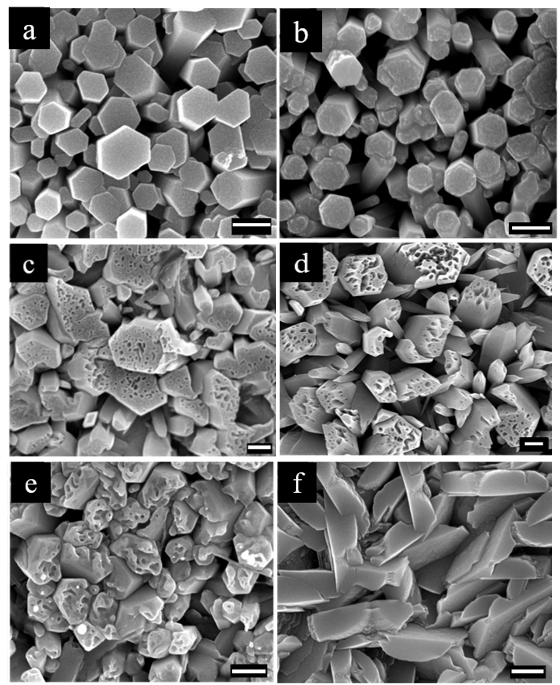
SEM images of bare ZNR and Au-ZNR with increasing concentrations of Au NPs are shown in Fig. 2 (a)-(f). The bare ZNRs show typical hexagonal nanorods with an average diameter of ) nm and uniform coverage across the Zn substrate. In contrast, Au-ZNR samples display distortion of the hexagonal shape and are riddled with pores (fig 1b-1e), with pore size and density increasing with increasing Au NP concentration. The pore size varies from 20 – 80 nm, which is comparable to the Au NP diameter. At the highest NP concentration (5AZn), the hexagonal shape is completely lost (Fig. 2(f)).
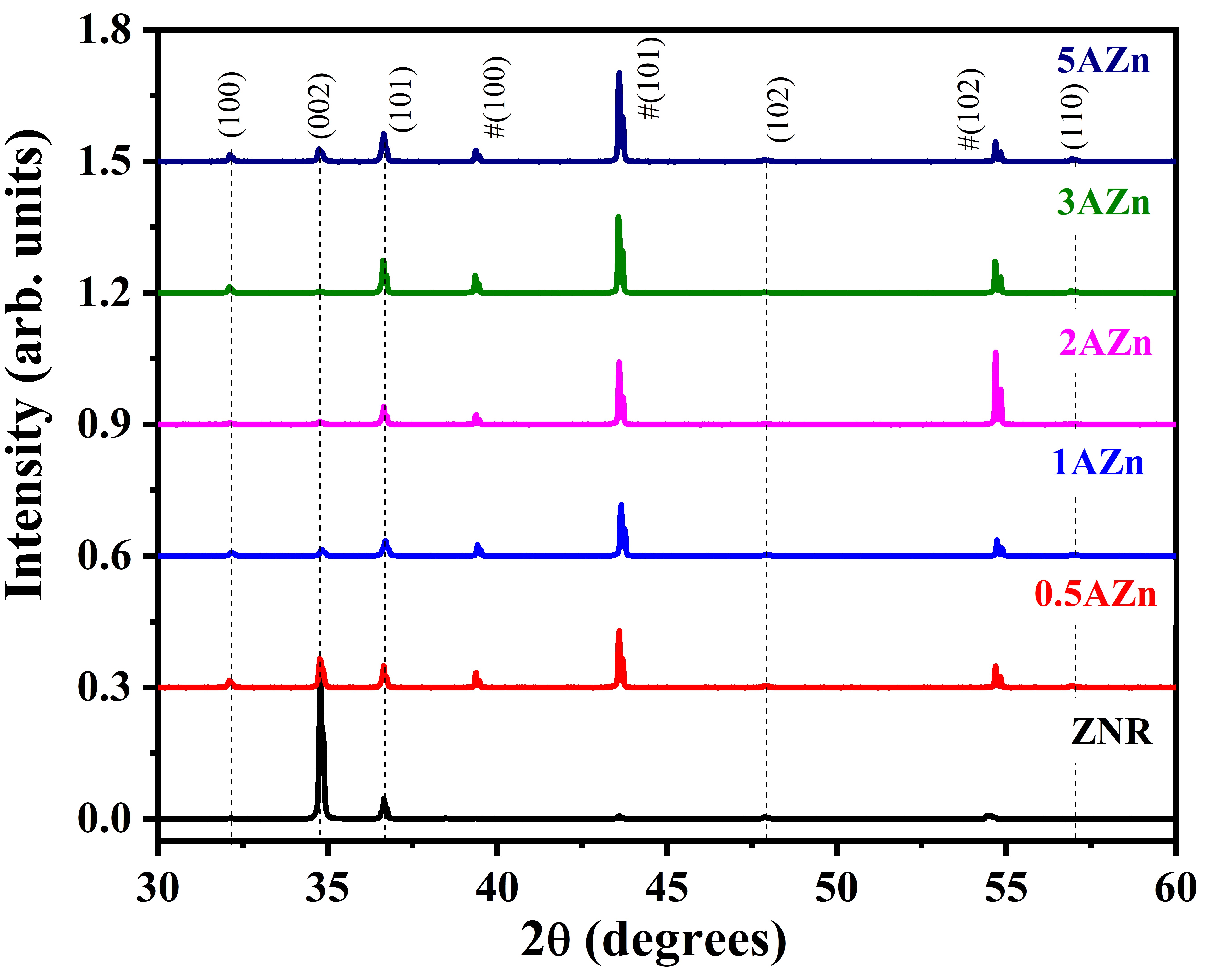
The evolution in morphology is reflected in the XRD spectra of the samples, shown in Fig. 3. The spectrum for the bare ZNRs shows a dominant ZnO (002) wurtzite peak along with less intense (100), (101) peaks and signatures of the Zn foil are marked with .
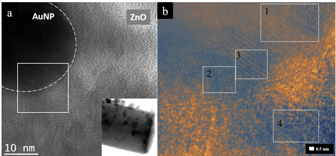
The spectra for AZn samples show increasingly impeded c-axis growth of the ZNRs and emerging signature of (100), (101), (102) and (110) planes of the ZnO lattice. It appears that the incorporation of each Au NP hinders the local c-axis growth of the ZnO crystallites, leading to the creation of pores, compromising the pristine hexagonal morphology. Low-resolution TEM images of an AZn sample, shown in Fig. 4(a), image the presence of Au NPs (dark regions of diameter 20-40 nm) on the surface and embedded within the ZNRs. Fig.4 (b) shows the HRTEM image of an AZn sample. The atomic planes of the nanorods and Au NPs are clearly evidenced by the fringe patterns. The c-axis oriented ZNRs shows commensurate planar spacing in the Fig.4 (b), simultaneously resolving the Au (111) planes of the AuNP, exhibiting fringe spacing of 0.28 and 0.22 nm, respectively. Fig.4 (c) shows magnified, contrast-enhanced image of the Au - ZnO interface evidencing the crossover from the Au to ZnO lattice. Regions 1 and 2 of Au NP show fringe width 0.23 nm while region 3 shows spacing between 0.22 nm to 0.24 nm. Region 4 shows fringe width 0.28 nm corresponding to the (002) plane of ZNR. The absence of any signature of Au lattice in the XRD data is perhaps due to the very low concentration of Au NPs in the system.
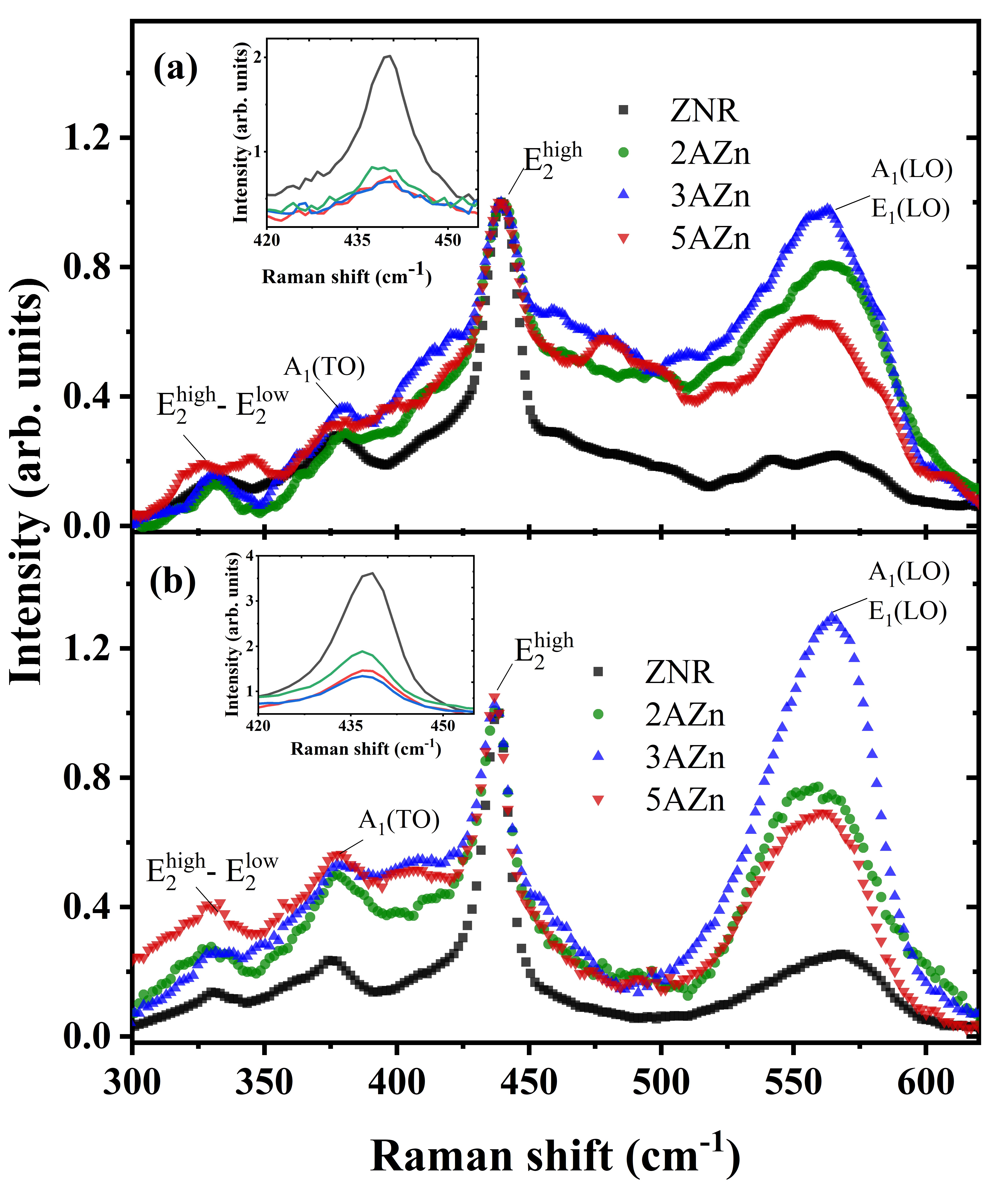
The Raman spectra of selected samples are shown in Fig.5, under 638 nm and 532 nm excitations. The in-plane motion of the O sub-lattice is indicated via the non-polar mode at 439 . Incorporation of Au NPs significantly compromises the intensity of the mode, as evidenced in the insets of Fig. 5. The Zinc sub-lattice vibration counterpart appears at around 99 (not shown).
The wurtzite structure also hosts the and modes, split into and branches. The broad peak centered at 560 is understood to be a convolution of the and modes along with contribution from Fröhlich optical phonon modes [51]. These polar modes are susceptible to the local electronic structure and thus sensitive to disorder via defect-induced doping. In the present samples, the feature around 560 increases in prominence with higher inclusion of Au NPs, i.e. samples 2AZn and 3AZn, due to increasing density of defects but then diminishes for the 5AZn sample. The disordered nature of the 5AZn sample with compromised growth leads to the breakdown of long range Fröhlich interaction[52], adversely affecting the intensity. Overall, modal intensity, in the 400 - 600 range, benefits from the presence of zone edge phonon modes that increase the phonon density of states [53]. An increase in intensity with NP inclusion is accompanied by increase in peak width that originates from defect-mediated relaxation of Raman selection rules [54]. The above understanding is further supported by the reproducibility of spectra recorded under both 638 nm and 532 nm excitation and across multiple samples. Under 532 nm excitation, the spectra in Fig. 5b benefit from localized surface plasmon-induced enhancement, especially the mixed mode peak centered at 560 . SM table S2 lists the wavenumbers for the various Raman modes of ZnO.
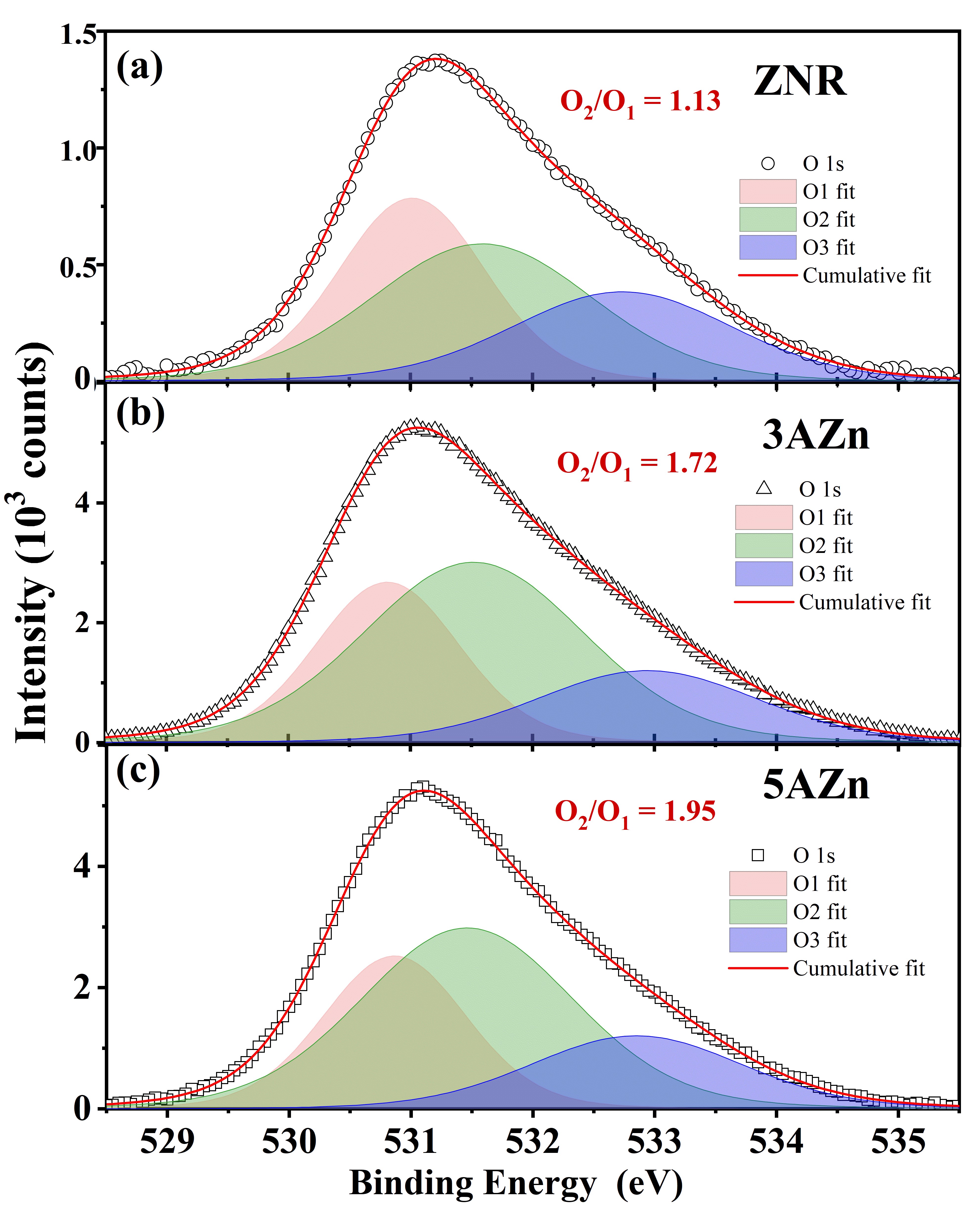
The relative abundance of defects and their evolution across the samples is obtained from XPS analysis. XPS spectra of the oxygen 1s state from bare ZNR and selected AuZNR samples are shown in Fig.6 (a)-(c). Each spectrum is deconvoluted to yield three peaks centred at 529 eV (O1), 530 eV (O2), and 532 eV (O3). While the O3 peak is understood to originate from surface contamination [55], the O1 and O2 correspond to binding energies of 1s electrons in O2- atoms in stoichiometrically pure and oxygen deficient regions of the lattice, respectively. The ratio of areas under the O2/O1 curves systematically increases across the samples and almost doubles for the 5AZn sample compared to bare ZNR, quantifying the monotonic increase in abundance upon inclusion of Au NPs.
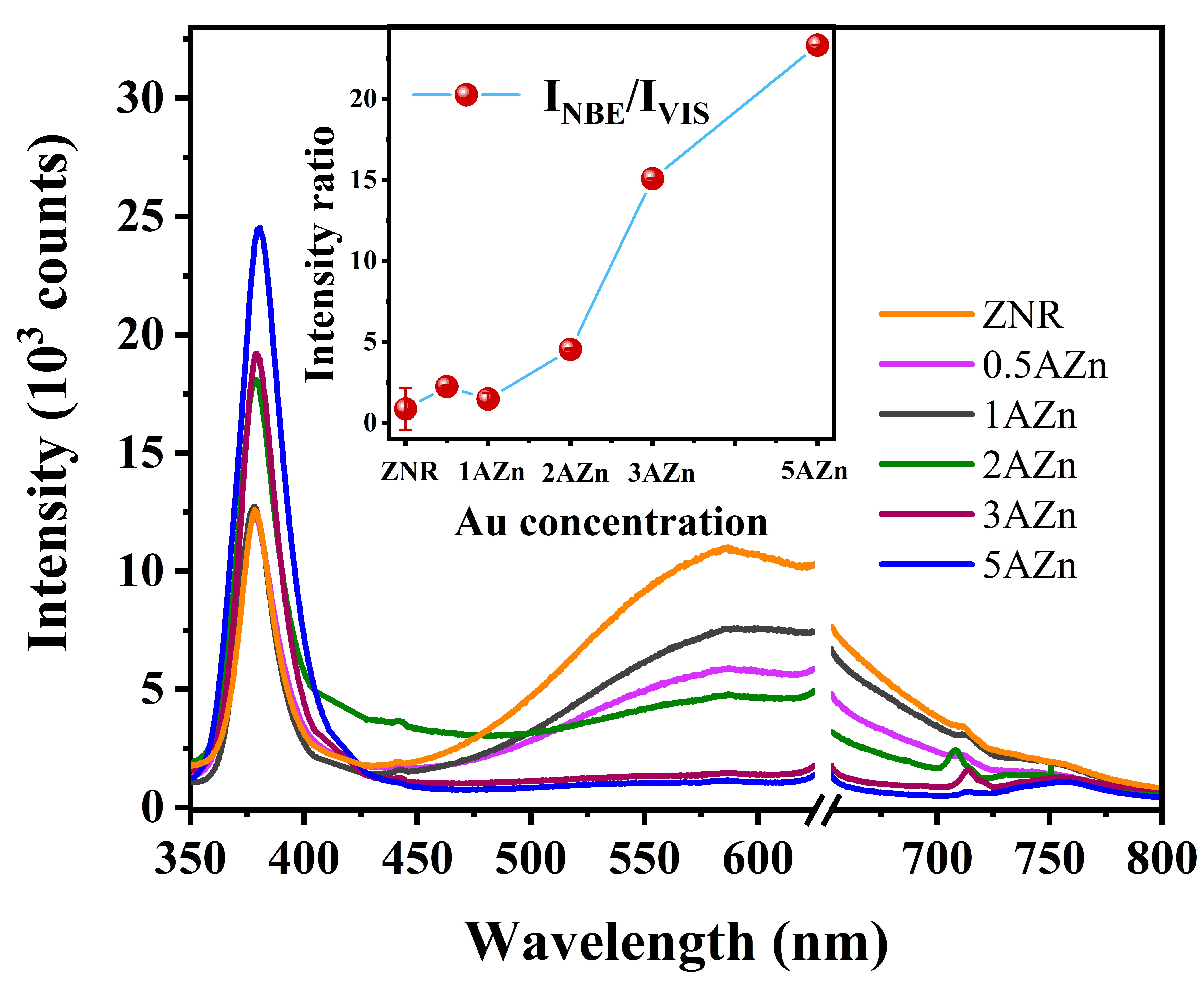
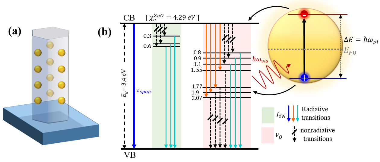
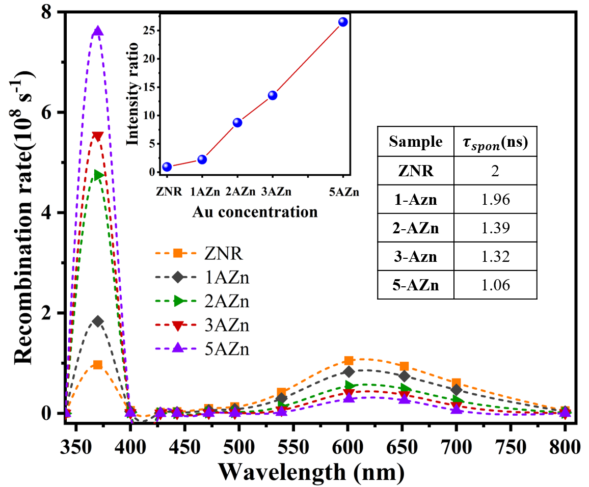
Inclusion of Au NPs in the ZNR matrix leads to changes in its morphology, crystal structure and stoichiometry, primarily nucleating higher density of and defects reflected in the PL spectra. Selected PL spectra (Fig.7) show that the NBE peak intensity progressively enhances with increasing AuNPs incorporation while the visible emission intensity decreases. The inset shows the change in intensity ratio that enhances with increasing Au NP inclusion, and by more than 20 for the 5AuZNR sample compared to the bare ZNR.[29, 56] Note that the enhancement varies across samples and these numbers are representative. The presence of the plasmonically active Au NPs strongly affects the spontaneous decay rates and, thus, luminescence from ZnO. For such low plasmonic resonances, the effect is spread over the 500 - 600 nm window, i.e. around the localized Surface Plasmon Resonance(SPR) wavelength of the 30 nm Au NP in ZnO matrix [29]. The physics of the excitation and photon emission under super band gap optical excitation are investigated via a 3D model of the system using FEM simulation in COMSOL Multiphysics using semi-classical formalism, combining the Semiconductor and Wave-Optics module of the software. Fig. 8a shows the in-scale model of ZnO nanorod embedded with Au NPs.
The PL spectrum of a bare -type ZNR, i.e. without any Au NP inclusion, is modeled with ten sub-band gap defect states, as shown in Fig. 8b. Each defect state is specified by its energy below the conduction band(CB), number density , and the electron and hole capture cross-sections and , respectively. Together they determine the electron and hole recombination rates associated with each defect level. Defect states with correspond to shallow levels arising from variously ionized and those with correspond to oxygen vacancy () states, with the states having the lowest energies. Under continuous wave super band gap energy excitation ( 320 nm), the model calculates the rate of stimulated absorption ( pair generation between the VB and CB). Assuming (i) a steady state is achieved between excitation and decay of pairs and (ii) that the Fermi-Dirac statistics adequately describe the distribution of electrons and holes across the energy states, albeit with different quasi-Fermi energies and , for electrons and holes respectively. Simulating the de-excitation process involves the calculation of various transition rates, including the spontaneous decay rate for direct CB to VB de-excitation that gives rise to NBE emission given by,
| (1) |
where and are the CB and VB electron occupation probabilities and (= 2 ns) is the spontaneous emission lifetime for ZnO [37, 57]. Similarly, rates for other transitions (Fig. 8b) from the CB edge to individual defect states (-capture) and from defect states to the VB edge (-capture) are calculated. We designate all transitions with emission energy () within the PL detection window (3.1 - 1.2 eV) as radiative transitions at the corresponding emission wavelength , and all other transitions as non-radiative. A plot of the transition rates vs. generates the simulated PL spectrum as shown in Fig. 9. The defect states at various are all assumed to have the same but different and . Typically, would be determined by the selection rules of transition between the states and show wide variation due to variability in local band bending and degree of ionization of the defect state. Broadly, would decrease with increasing defect state energy difference with the conduction or valence band involved in the radiative transition (Fig. S1 )[58].
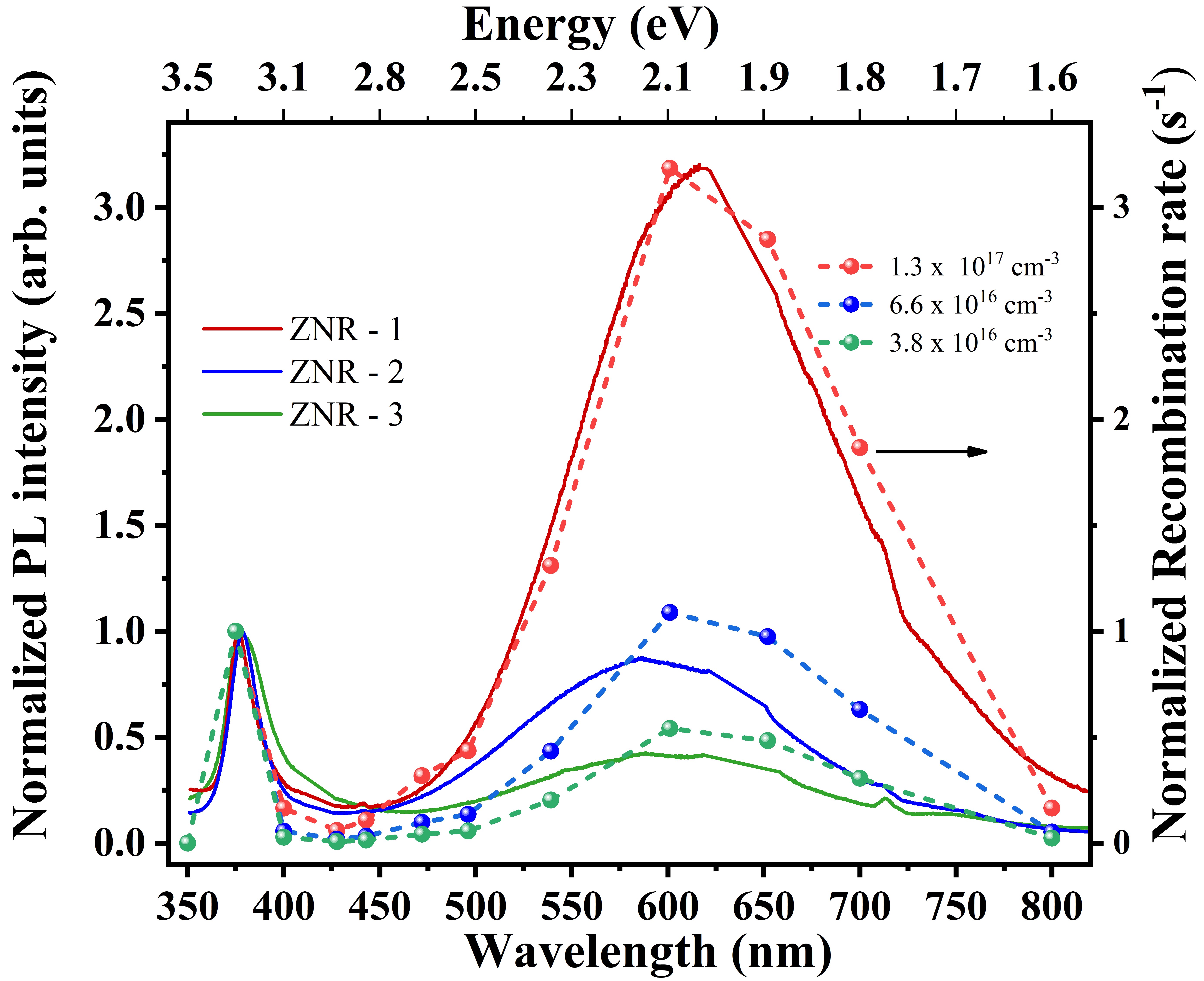
Here, variation of alone controls the intensity of visible to NBE emission and is used to mimic the experimentally observed variation across samples (Fig. 9), as shown by the blue spectra in Fig. 1. We proceed with /cc that mimics PL of samples showing . Details of the simulation, including model geometry and material parameters used are available in SM Section S3.
For the hybrid system, inclusion of Au NPs in ZNRs and UV photoexcitation induce systemic changes that include (i) increase in overall defect density in ZNRs due to increased disorder, (ii) creation of Schottky barriers at the Au-ZnO boundaries, (iii) absorption of ZnO visible PL in the near field by the NPs to generate LSPs, (iv) LSP decay induced hot carrier generation in Au NPs and transfer to ZnO, and finally (v) cumulative modulation in PL spectrum of the hybrid samples.
The PL spectrum from bare ZNRs may be alternatively simulated using a classical dipole emission model by defining a dipole current density () distributed throughout the volume of the ZNRs [29]. The spectral variation of the dipole moment is given as , where is the experimentally recorded PL spectrum of bare ZNR. Beginning with the simulated PL spectrum corresponding to sample ZNR-2 in Fig. 9, the PL spectral evolution upon inclusion of Au NPs within the ZNR geometry (Fig.8(a)) is shown in Fig. S2(SM Section S3). With increasing Au NP density the changes negligibly and the decrease in is far muted than that observed experimentally, demonstrating that plasmonic absorption, modeled using classical electrodynamics alone does not account for the observed quenching of visible emission. Within the semi-classical framework, the work function of Au (), along with the electron affinity of ZnO () set the energy scale of the hybrid system. At equilibrium without any photoexcitation, solution of the Poisson equation shows that the CB edge in the -type ZnO bends upwards at the Au-ZnO interface creating a Schottky barrier and local depletion in (SM Fig. S3). However, upon super band gap excitation ( 320 nm), the increase in photoexcited carriers induces a nonequilibrium steady state in ZnO, increasing with the CB edge bending down by 0.15 eV below its flat band energy, as shown in Fig. 10 (see SM Section S4 for further details).

The visible component () of the ensuing PL (Fig. 9), with strong overlap with the absorption of the NPs, excites LSPs of energy . Once excited, the LSPs dephase in the time scale 10 fs [59, 60] and decay radiatively and non-radiatively, depending on NP size [9]. In smaller NPs, the latter dominates causing pair generation and subsequent thermalization with 0.1 - 100s of ps [61]. Under continuous excitation, hot carriers in the NPs reach a steady state, non-equilibrium distribution , that departs significantly from the equilibrium distribution in the energy range , where is the Fermi energy prior to photoexcitation [62, 10, 63]. For spherical NPs, may be determined from Eq. 2, following Kornbluth et al. [64];
| (2) |
where is the number density of plasmons absorbed per unit time, is a relaxation time constant, is the density of states, and . The left panel of Fig. 10 plots calculated for = 5.1 eV at 300 K and = 2.3 eV(see SM Section S5 for further details). is determined by several parameters including the number of embedded Au NPs, intensity of visible emission from ZnO, which is dependent on the intensity of the UV excitation (). Finally the quantum efficiency of hot carrier generation and the fraction transferred to ZnO, aided by the downward band bending at the interface determine . SM Fig. S5 plots the for various values of and . Hot electrons transferred to the ZnO CB would enhance NBE emission, which is incorporated in the present model by recalculating (Eq. 1) by modifying the ZnO CB occupation by addition of distribution of electrons. The increased rate is given as:
| (3) |
Increasing Au NP density across samples is reflected in via increasing in Eq. 2, which is guided by the experimentally detected NBE emission enhancement. The increase in is reflected in time resolved PL measurements that show a decrease in NBE spontaneous emission life-time as summarized in SM table S6 in the presence of plasmonic NPs [36, 31, 32, 33, 34]. Recalculating the transition rates with and thus thus incorporates the hot electron contribution from NP inclusion, which intensifies NBE emission and provides a direct coupling that quantifies the cross-talk between the components. The nonequilibrium steady state reached under CW photoexcitation also modifies the probability of electron occupation across the defect states. Though is assumed to be the same across the defect states, the number changes dynamically under photoexcitation, affecting the kinetics of the PL process. SM Fig. S4 plots the occupancy of the states before and after hot electron transfer showing that DL state occupancy 1, with two consequences. Firstly, the ionized DL defect states () under high occupancy cease to exist at the designated energies, selectively reducing their individual . The abundance and occupation of defect states is non-trivial to estimate, especially with photoexcitation. The simulation uses Shockley-Read-Hall statistics to calculate the probability of occupation of the defect states [65]. At equilibrium the fraction of any ionized donor species is given by [66].
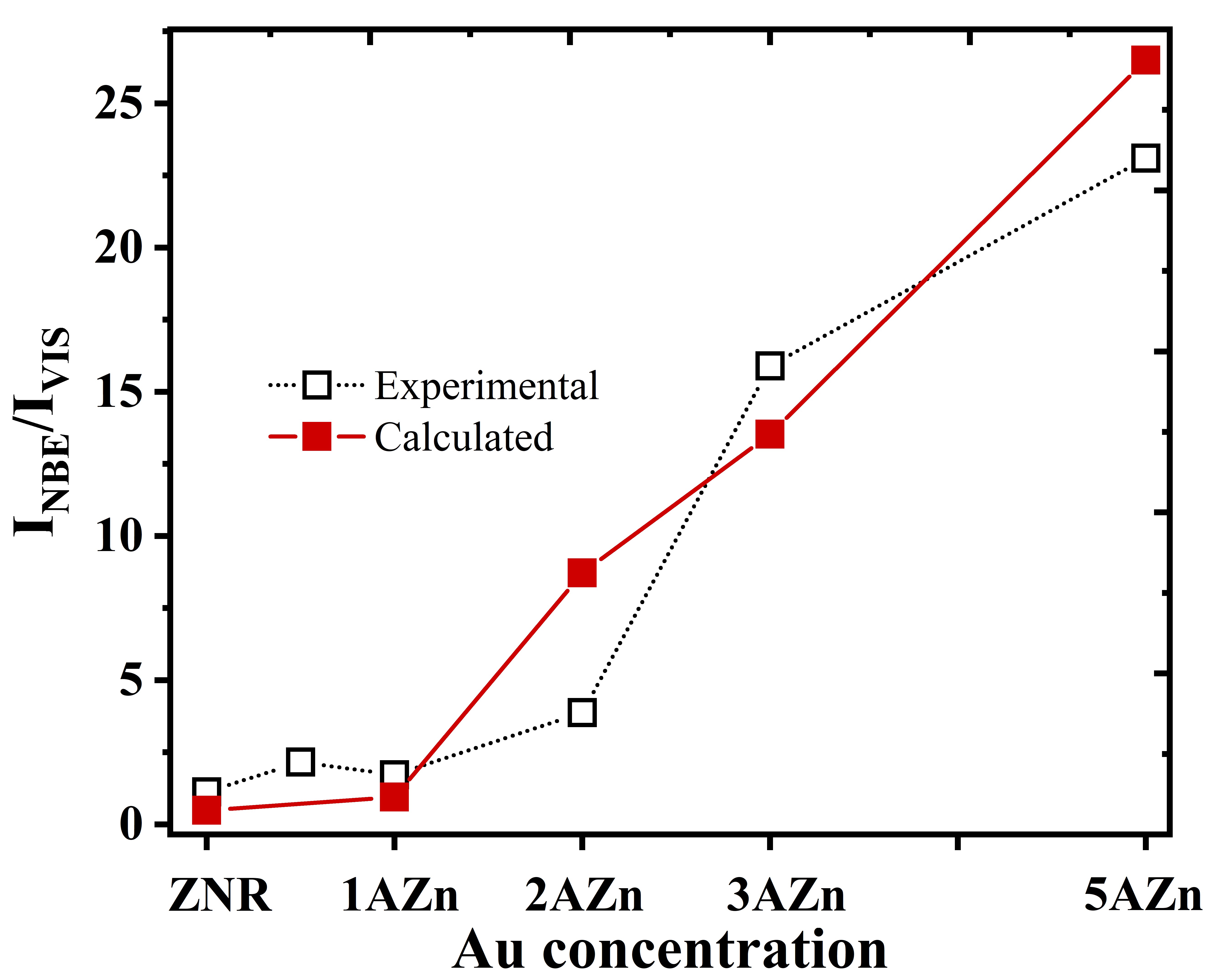
Under photoexcitation, lies closer to , decreasing and quenching the relative abundance of the DL ionized defect states, as discussed above. Secondly, the energy proximity of the DL states with indicates presence of non-radiative charge transfer pathways between Au and ZnO. Hot holes may diffuse and recombine with DL state electrons or vice-versa, thereby reducing the availability of DL electrons, compromising both NBE and visible emission [37]. Under CW illumination, these competing processes would reach a steady state, compromising radiative transitions to and from the DL states in ZnO and thus, visible emission. The condition is mimicked in the simulation by a decrease in preferentially for the states with occupancy close to 1. Beginning with model parameters for bare ZNR that yield comparable maximum recombination rates for NBE and visible emission, Fig.11 plots the evolution with increasing Au NP inclusion. As progressively increases, raising , decrease in s for selected DL states based on calculated occupancy of the states decrease visible emission. The table in the inset of Fig.11 lists the calculated decrease in with the changing parameters. The efficacy of the simulations and optimal choice of parameters in modeling experimental results are further shown in Fig.12, which plots the ratio for samples with increasing Au NP density across the experimental and simulated results. Agreement between the results evidence the capability model in capturing the key ingredients of light-matter interactions discussed here.
Though the experimental results modeled here follow previous reports [31, 32, 33, 34, 35, 36, 37] the near complete quenching of visible emission has not been reported earlier. Size and density of the plasmonic inclusions play a crucial role in determining their effect on the PL of the semiconductor. Increasing NP density above a threshold leads to quenching of PL due to charge transfer from ZnO to Au NPs [25], which is controlled via both geometric parameters and the nature of band alignment across the components [29]. Further, increase in UV excitation () intensity enhances PL NBE emission more than visible emission in plasmonic hybrids, in contrast to bare ZnO where both components are seen to increase in tandem [37]. In the model, intensity increase if effected via increasing , which again selectively enhances the NBE emission more than the visible.
IV Conclusion
This investigation models the photoluminescence of an Au - ZnO hybrid plasmonic system using a semiclassical model, employing finite element method calculations. Experimental results evidence complete quenching of visible emission and simultaneous increase in NBE emission intensity, with increasing Au NP inclusion in ZnO nanorods. The result is non-trivial since inclusion of Au NPs substantially increases morphological disorder in the ZnO lattice and increases oxygen defect density as investigated by a combination of structural and spectroscopic probes. The model, incorporating ZnO’s band properties with sub-bandgap defect states, reproduces the photoluminescence from bare ZnO nanorods and its variation across samples. The effect of plasmonic NPs under UV excitation is incorporated via calculating localized surface plasmon-mediated hot electron generation in Au and subsequent transfer to the conduction band of ZnO, thus enhancing NBE emission. Finally, reduction in visible emission is partially attributed to near-field absorption by the Au NPs and partially to passivation of the deep-level ionized defect states due to high electron occupancy under photoexcitation and non-radiative charge transfer to Au NPs. Overall, the model successfully combines the photo-stimulated excitation and de-excitation processes in a wide band gap semiconductor with plasmon-mediated hot electron generation in metal nanoparticles to simulate the evolution of photoluminescence spectra of the semiconductor. With increasing interest in hybrid plasmonic systems and novel applications, the results offer a modeling platform for engineering their optoelectronic and photocatalytic properties.
Acknowledgements.
The authors thank Harikrishnan G. (IISER TVM) for valuable inputs on XPS analysis. The authors acknowledge ISTEM, Govt. of India for access to COMSOL Multiphysics software and financial support from SERB, Govt. of India (CRG/2019/004965). KS and SC acknowledge PhD fellowship from IISER TVM.KS and SC contributed equally to this work.
References
- Kalathingal et al. [2016] V. Kalathingal, P. Dawson, and J. Mitra, Scanning tunneling microscope light emission: Effect of the strong dc field on junction plasmons, Phys. Rev. B 94, 035443 (2016).
- Maier [2007] S. A. Maier, Localized surface plasmons, in Plasmonics: Fundamentals and Applications, edited by S. A. Maier (Springer US, New York, NY, 2007) pp. 65–88.
- Pelton [2015] M. Pelton, Modified spontaneous emission in nanophotonic structures, Nature Photonics 9, 427 (2015).
- Wu et al. [2015] K. Wu, J. Chen, J. R. McBride, and T. Lian, Efficient hot-electron transfer by a plasmon-induced interfacial charge-transfer transition, Science 349, 632 (2015).
- Boyle et al. [2009] M. G. Boyle, J. Mitra, and P. Dawson, The tip–sample water bridge and light emission from scanning tunnelling microscopy, Nanotechnology 20, 335202 (2009).
- Kalathingal et al. [2017] V. Kalathingal, P. Dawson, and J. Mitra, Scanning tunnelling microscope light emission: Finite temperature current noise and over cut-off emission, Sci Rep 7, 3530 (2017).
- Lee et al. [2012] S.-Y. Lee, I.-M. Lee, J. Park, S. Oh, W. Lee, K.-Y. Kim, and B. Lee, Role of magnetic induction currents in nanoslit excitation of surface plasmon polaritons, Phys. Rev. Lett. 108, 213907 (2012).
- Jimbo and Imura [2022] A. Jimbo and K. Imura, Nonlinear photoluminescence from gold nanoparticle thin films studied by scanning near-field optical microscopy, The Journal of Physical Chemistry C 126, 14960 (2022).
- Mertens et al. [2017] J. Mertens, M. E. Kleemann, R. Chikkaraddy, P. Narang, and J. J. Baumberg, How Light Is Emitted by Plasmonic Metals, Nano Letters 17, 2568 (2017).
- Brown et al. [2016] A. M. Brown, R. Sundararaman, P. Narang, W. A. Goddard, and H. A. Atwater, Nonradiative plasmon decay and hot carrier dynamics: Effects of phonons, surfaces, and geometry, ACS Nano 10, 957 (2016).
- Pinchuk and Kreibig [2003] A. Pinchuk and U. Kreibig, Interface decay channel of particle surface plasmon resonance, New Journal of Physics 5, 151 (2003).
- Link and El-Sayed [1999] S. Link and M. A. El-Sayed, Spectral properties and relaxation dynamics of surface plasmon electronic oscillations in gold and silver nanodots and nanorods, The Journal of Physical Chemistry B 103, 8410 (1999).
- Cao et al. [2007] L. Cao, D. N. Barsic, A. R. Guichard, and M. L. Brongersma, Plasmon-assisted local temperature control to pattern individual semiconductor nanowires and carbon nanotubes, Nano Letters 7, 3523 (2007).
- Cui et al. [2020] L. Cui, Y. Zhu, M. Abbasi, A. Ahmadivand, B. Gerislioglu, P. Nordlander, and D. Natelson, Electrically driven hot-carrier generation and above-threshold light emission in plasmonic tunnel junctions, Nano Letters 20, 6067 (2020).
- Olson et al. [2015] J. Olson, S. Dominguez-Medina, A. Hoggard, L.-Y. Wang, W.-S. Chang, and S. Link, Optical characterization of single plasmonic nanoparticles, Chem. Soc. Rev. 44, 40 (2015).
- Clavero [2014] C. Clavero, Plasmon-induced hot-electron generation at nanoparticle/metal-oxide interfaces for photovoltaic and photocatalytic devices, Nature Photonics 8, 95 (2014).
- Li and Valentine [2017] W. Li and J. G. Valentine, Harvesting the loss: surface plasmon-based hot electron photodetection, 6, 177 (2017).
- Linic et al. [2021] S. Linic, S. Chavez, and R. Elias, Flow and extraction of energy and charge carriers in hybrid plasmonic nanostructures, Nature Materials 20, 916 (2021).
- Mali et al. [2016] S. S. Mali, C. S. Shim, H. Kim, P. S. Patil, and C. K. Hong, In situ processed gold nanoparticle-embedded tio2 nanofibers enabling plasmonic perovskite solar cells to exceed 14efficiency, Nanoscale 8, 2664 (2016).
- Chen et al. [2008] T. Chen, G. Z. Xing, Z. Zhang, H. Y. Chen, and T. Wu, Tailoring the photoluminescence of zno nanowires using au nanoparticles, Nanotechnology 19, 435711 (2008).
- Kim et al. [2021] D. W. Kim, K. H. Park, S.-H. Lee, C. Fàbrega, J. D. Prades, and J.-W. Jang, Plasmon expedited response time and enhanced response in gold nanoparticles-decorated zinc oxide nanowire-based nitrogen dioxide gas sensor at room temperature, Journal of Colloid and Interface Science 582, 658 (2021).
- Suematsu et al. [2018] K. Suematsu, K. Watanabe, A. Tou, Y. Sun, and K. Shimanoe, Ultraselective toluene-gas sensor: Nanosized gold loaded on zinc oxide nanoparticles, Analytical Chemistry 90, 1959 (2018).
- Bora et al. [2016] T. Bora, D. Zoepfl, and J. Dutta, Importance of plasmonic heating on visible light driven photocatalysis of gold nanoparticle decorated zinc oxide nanorods, Scientific Reports 6, 26913 (2016).
- Castelló Lux et al. [2023] K. Castelló Lux, J. Hot, P. Fau, A. Bertron, M. L. Kahn, E. Ringot, and K. Fajerwerg, Nano-gold decorated zno: An alternative photocatalyst promising for nox degradation, Chemical Engineering Science 267, 118377 (2023).
- Chiu et al. [2018] Y.-H. Chiu, K.-D. Chang, and Y.-J. Hsu, Plasmon-mediated charge dynamics and photoactivity enhancement for au-decorated zno nanocrystals, J. Mater. Chem. A 6, 4286 (2018).
- Bandopadhyay and Mitra [2015] K. Bandopadhyay and J. Mitra, Zn interstitials and O vacancies responsible for n-type ZnO: what do the emission spectra reveal?, RSC Advances 5, 23540 (2015).
- Kang et al. [2021] Y. Kang, F. Yu, L. Zhang, W. Wang, L. Chen, and Y. Li, Review of zno-based nanomaterials in gas sensors, Solid State Ionics 360, 115544 (2021).
- Bandopadhyay and Mitra [2016] K. Bandopadhyay and J. Mitra, Spatially resolved photoresponse on individual zno nanorods: correlating morphology, defects and conductivity, Scientific Reports 6, 28468 (2016).
- Prajapati et al. [2020] K. N. Prajapati, B. Johns, K. Bandopadhyay, S. R. P. Silva, and J. Mitra, Interaction of ZnO nanorods with plasmonic metal nanoparticles and semiconductor quantum dots, Journal of Chemical Physics 152, 64704 (2020).
- Cheng et al. [2010] C. W. Cheng, E. J. Sie, B. Liu, C. H. A. Huan, T. C. Sum, H. D. Sun, and H. J. Fan, Surface plasmon enhanced band edge luminescence of zno nanorods by capping au nanoparticles, Applied Physics Letters 96, 071107 (2010).
- Ziani et al. [2022] A. Ziani, S. Al-Taweel, M. A. Nadeem, and H. Idriss, Effect of gold loading on time-resolved ps photoluminescence of zno, The Journal of Physical Chemistry C 126, 16148 (2022).
- Fiedler et al. [2020a] S. Fiedler, L. O. L. C. Lem, C. Ton-That, M. Schleuning, A. Hoffmann, and M. R. Phillips, Correlative study of enhanced excitonic emission in zno coated with al nanoparticles using electron and laser excitation, Scientific Reports 10, 2553 (2020a).
- Kiba et al. [2016] T. Kiba, K. Yanome, M. Kawamura, Y. Abe, K. H. Kim, J. Takayama, and A. Murayama, Emission enhancement in indium zinc oxide(izo)/ag/izo sandwiched structure due to surface plasmon resonance of thin ag film, Applied Surface Science 389, 906 (2016).
- Fiedler et al. [2020b] S. Fiedler, L. O. Lee Cheong Lem, C. Ton-That, A. Hoffmann, and M. R. Phillips, Enhancement of the uv emission from gold/zno nanorods exhibiting no green luminescence, Optical Materials Express 10, 1476 (2020b).
- Khan et al. [2019] R. Khan, P. Uthirakumar, T. H. Kim, and I.-H. Lee, Enhanced photocurrent performance of partially decorated au nanoparticles on zno nanorods based uv photodetector, Materials Research Bulletin 115, 176 (2019).
- Wang et al. [2021] X. Wang, Q. Ye, L.-H. Bai, X. Su, T.-T. Wang, T.-W. Peng, X.-Q. Zhai, Y. Huo, H. Wu, C. Liu, Y.-Y. Bu, X.-H. Ma, Y. Hao, and J.-P. Ao, Enhanced uv emission from zno on silver nanoparticle arrays by the surface plasmon resonance effect, Nanoscale Research Letters 16, 8 (2021).
- Guidelli et al. [2015] E. J. Guidelli, O. Baffa, and D. R. Clarke, Enhanced uv emission from silver/zno and gold/zno core-shell nanoparticles: Photoluminescence, radioluminescence, and optically stimulated luminescence, Scientific Reports 5, 14004 (2015).
- Singh et al. [2023] D. K. Singh, P. Prajapat, J. Saroha, R. K. Pant, S. N. Sharma, K. K. Nanda, S. B. Krupanidhi, and G. Gupta, Photocurrent polarity switching and enhanced photoresponse in silver nanoparticles decorated a-gan-based photodetector, ACS Applied Electronic Materials 5, 1394 (2023).
- Prajapati et al. [2022] K. N. Prajapati, A. A. Nair, J. Fernandes, S. R. P. Silva, and J. Mitra, Imaging with raman photons: a novel use of mixed-mode spectroscopy, Nano Express 3, 035007 (2022).
- Wang et al. [2023] X. Wang, S. Gao, and J. Ma, Schottky barrier effect on plasmon-induced charge transfer, Nanoscale 15, 1754 (2023).
- Shi et al. [2013] X. Shi, K. Ueno, N. Takabayashi, and H. Misawa, Plasmon-enhanced photocurrent generation and water oxidation with a gold nanoisland-loaded titanium dioxide photoelectrode, The Journal of Physical Chemistry C 117, 2494 (2013).
- Strelow et al. [2016] C. Strelow, T. S. Theuerholz, C. Schmidtke, M. Richter, J.-P. Merkl, H. Kloust, Z. Ye, H. Weller, T. F. Heinz, A. Knorr, and H. Lange, Metal–semiconductor nanoparticle hybrids formed by self-organization: A platform to address exciton–plasmon coupling, Nano Letters 16, 4811 (2016).
- Ratchford et al. [2017] D. C. Ratchford, A. D. Dunkelberger, I. Vurgaftman, J. C. Owrutsky, and P. E. Pehrsson, Quantification of efficient plasmonic hot-electron injection in gold nanoparticle–tio2 films, Nano Letters 17, 6047 (2017).
- Vogel and Kilin [2015] D. J. Vogel and D. S. Kilin, First-principles treatment of photoluminescence in semiconductors, The Journal of Physical Chemistry C 119, 27954 (2015).
- Zhou et al. [2019] N. Zhou, B. C. Hu, Q. Y. Zhang, C. Y. Ma, and S. Z. Hao, Theoretical model of excitonic luminescence and its application to the study of fine structure and exciton dynamics in zno, Journal of Applied Physics 126, 165701 (2019).
- Lyons et al. [2017] J. L. Lyons, J. B. Varley, D. Steiauf, A. Janotti, and C. G. Van de Walle, First-principles characterization of native-defect-related optical transitions in zno, Journal of Applied Physics 122, 035704 (2017).
- Li [2017] L. Li, On the double-band luminescence of zno nanoparticles, Europhysics Letters 117, 67005 (2017).
- Campbell et al. [2019] B. Campbell, E. Zarate, P. Kelly, and L. Kuznetsova, Three-level system for numerical modeling of ultraviolet and visible photoluminescence of aluminum-doped zinc oxide, Journal of the Optical Society of America B 36, 1017 (2019).
- Mertens et al. [2007] H. Mertens, A. F. Koenderink, and A. Polman, Plasmon-enhanced luminescence near noble-metal nanospheres: Comparison of exact theory and an improved gersten and nitzan model, Physical Review B 76, 115123 (2007).
- Rakić et al. [1998] A. D. Rakić, A. B. Djurišić, J. M. Elazar, and M. L. Majewski, Optical properties of metallic films for vertical-cavity optoelectronic devices, Appl. Opt. 37, 5271 (1998).
- Cuscó et al. [2007] R. Cuscó, E. Alarcón-Lladó, J. Ibáñez, L. Artús, J. Jiménez, B. Wang, and M. J. Callahan, Temperature dependence of raman scattering in , Physical Review B 75, 165202 (2007).
- Gandhi et al. [2018] A. C. Gandhi, W.-S. Yeoh, M.-A. Wu, C.-H. Liao, D.-Y. Chiu, W.-L. Yeh, and Y.-L. Huang, New insights into the role of weak electron–phonon coupling in nanostructured zno thin films, 8, 632 (2018).
- Serrano et al. [2004] J. Serrano, A. H. Romero, F. J. Manjón, R. Lauck, M. Cardona, and A. Rubio, Pressure dependence of the lattice dynamics of zno: An ab initio approach, Phys. Rev. B 69, 094306 (2004).
- Šćepanović et al. [2010] M. Šćepanović, M. Grujić-Brojčin, K. Vojisavljević, S. Bernikc, and T. Srećković, Raman study of structural disorder in ZnO nanopowders, Journal of Raman Spectroscopy 41, 914 (2010).
- Kayaci et al. [2014] F. Kayaci, S. Vempati, I. Donmez, N. Biyikli, and T. Uyar, Role of zinc interstitials and oxygen vacancies of ZnO in photocatalysis: A bottom-up approach to control defect density, Nanoscale 6, 10224 (2014).
- Shubina et al. [2010] T. V. Shubina, A. A. Toropov, V. N. Jmerik, D. I. Kuritsyn, L. V. Gavrilenko, Z. F. Krasil’nik, T. Araki, Y. Nanishi, B. Gil, A. O. Govorov, and S. V. Ivanov, Plasmon-induced purcell effect in inn/in metal-semiconductor nanocomposites, Phys. Rev. B 82, 073304 (2010).
- Galdámez-Martínez et al. [2022] A. Galdámez-Martínez, A. Dutt, M. Jain, L. Bazán-Díaz, G. Santana, A. Méndez-Blas, and O. de Melo, Decay emission study of zno nanostructures obtained by low-pressure vapor transport technique, Applied Surface Science Advances 12, 100334 (2022).
- Ryan et al. [2015] J. T. Ryan, A. Matsuda, J. P. Campbell, and K. P. Cheung, Interface-state capture cross section—Why does it vary so much?, Applied Physics Letters 106, 163503 (2015).
- Brongersma et al. [2015] M. L. Brongersma, N. J. Halas, and P. Nordlander, Plasmon-induced hot carrier science and technology, Nature Nanotechnology 10, 25 (2015).
- Voisin et al. [2001] C. Voisin, N. D. Fatti, D. Christofilos, and F. Vallee, Ultrafast electron dynamics and optical nonlinearities in metal nanoparticles, Journal of Physical Chemistry B 105, 2264 (2001).
- Furube et al. [2007] A. Furube, L. Du, K. Hara, R. Katoh, and M. Tachiya, Ultrafast plasmon-induced electron transfer from gold nanodots into TiO2 nanoparticles, Journal of the American Chemical Society 129, 14852 (2007).
- Bernardi et al. [2015] M. Bernardi, J. Mustafa, J. B. Neaton, and S. G. Louie, Theory and computation of hot carriers generated by surface plasmon polaritons in noble metals, Nature Communications 6, 7044 (2015).
- Besteiro et al. [2017] L. V. Besteiro, X. T. Kong, Z. Wang, G. Hartland, and A. O. Govorov, Understanding Hot-Electron Generation and Plasmon Relaxation in Metal Nanocrystals: Quantum and Classical Mechanisms, ACS Photonics 4, 2759 (2017).
- Kornbluth et al. [2013] M. Kornbluth, A. Nitzan, and T. Seideman, Light-induced electronic non-equilibrium in plasmonic particles, J. Chem. Phys 138, 174707 (2013).
- [65] E. H. Rhoderick and R. H. Williams, Metal-semiconductor contacts (Oxford Univ. Press, 1988).
- Sze and Ng [2006] S. Sze and K. K. Ng, Physics and properties of semiconductors—a review, in Physics of Semiconductor Devices, edited by S. Sze and K. K. Ng (John Wiley & Sons, Ltd, Hoboken, NJ, 2006) pp. 5–75.