Towards understanding the electronic structure of the simpler members of two-dimensional halide-perovskites
Abstract
In this paper we analyze the band-structure of two-dimensional (2D) halide perovskites by considering structures related to the simpler case of the series, (BA)2PbI4, in which PbI4 layers are intercalated with butylammonium (BA=CH3(CH2)3NH3) organic ligands. We use density-functional-theory (DFT) based calculations and tight-binding (TB) models aiming to discover a simple description of the bands within 1 eV below the valence-band maximum and 2 eV above the conduction-band minimum, which, including the energy gap, is about a eV energy range. The bands in this range are those expected to contribute to the transport phenomena, photoconductivity and light-emission in the visible spectrum, at room and low temperature. We find that the atomic orbitals of the butylammonium chains have negligible contribution to the Bloch states which form the conduction and valence bands in the above defined range. Our calculations reveal a rather universal, i.e., independent of the intercalating BA, rigid-band picture inside the above range characteristic of the layered perovskite “matrix” (i.e., PbI4 in our example). Besides demonstrating the above conclusion, the main goal of this paper is to find accurate TB models which capture the essential features of the DFT bands in this range. First, we ignore electron hopping along the -axis and the octahedral distortions and this increased symmetry (from C2 to C4) halves the Bravais-lattice unit-cell size and the Brillouin zone unfolds to a 45∘ rotated square and this allows some analytical handling of the 2D TB-Hamiltonian. The Pb and I orbitals are far away from the above range and, thus, we integrate them out to obtain an effective model which only includes hybridized Pb and I states. Our TB-based treatment a) provides a good quantitative description of the DFT band-structure, b) helps us conceptualize the complex electronic structure in the family of these materials in a simple way and c) yields the one-body part to be combined with appropriately screened electron interaction to describe many-body effects, such as, excitonic bound-states.
I Introduction
The discovery and production of semiconducting superlattices has led to a significant advancement in solid-state physics and electronic technology. Further development, however, has been hindered by the infrastructure-demanding time-consuming fabrication procedure for precisely assembling the nanometer-scale structures in such artificial material structures. Rather recently, a new class of superlattices has been discovered, known as Ruddlesden-Popper (RP) two-dimensional (2D) halide-perovskites, that can be self-assembled using wet-chemistry synthesis[1, 2]. The interest in this type of materials is not just because of the simplicity of the synthesis process, but more importantly, the interest is due to the fact that they are clean and maintain the periodic structure at the atomic level.
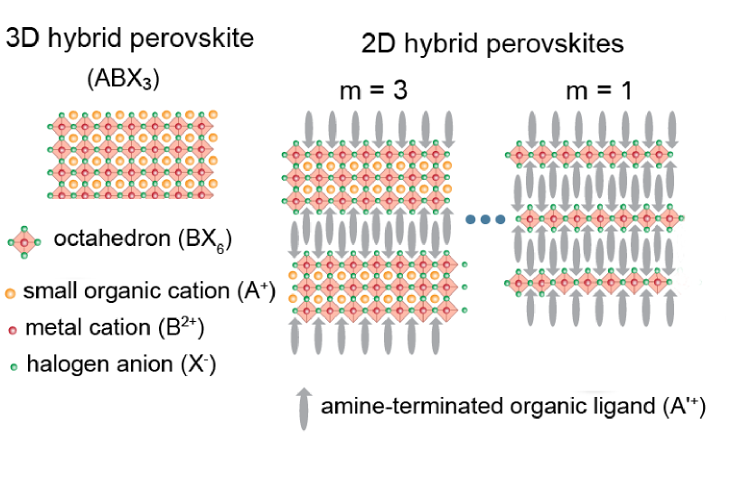
These 2D halide-perovskites are analogues to the oxide perovskites described by Ruddlesden and Popper[3], from where they gain their name, and they form self-assembled superlattice structures[1, 4, 5, 6]. Fig. 1 illustrates the relationship of the Ruddlesden-Popper perovskite structures to the three-dimensional (3D) perovskite ABX3, where A B and X are, a small organic cation (such as methylammonium), a metal cation and a halogen anion respectively. The bulk perovskite ABX3 is figuratively sliced apart to form a multilayer sandwich in which amine-terminated organic ligands A′ (such as, butylammonium) are “inserted” in between every m (m=1,2,…) adjacent halide-perovskite layers (see Fig. 1) in the formula AAm-1BmX3m+1. An example of this series is the family[1, 2] (BA)2(MA)m-1PbmI3m+1 with BA=CH3(CH2)3NH3 and MA=CH3NH3 (m = 1, 2, 3, 4, …). These Ruddlesden-Popper hybrid perovskites come with inherent low dimensionality and highly ordered periodic nanostructures. The amine-terminated organic ligands essentially cleave the 3D perovskite lattices into two-dimensional sheets, forming alternating layers of organic and inorganic supercells along the -axis crystal orientation. The formation of such layered structures is thermodynamically favorable, which makes it possible to obtain Ruddlesden-Propper hybrid perovskites conveniently using wet-chemistry synthesis.
The family of 3D organic halide-perovskites has received tremendous attention during the past decade due to their promising optoelectronic and solar cell applications. Decreasing the dimensionality from 3D to 2D, more versatile organic cations can be incorporated as templates to produce new structures[7]. The properties of these reduced dimensionality semiconductors are less widely studied but results of many such studies have started to appear in the literature rapidly. Among the many fascinating properties of these materials is white-light emission[8], where the broad emission comes from the transient photoexcited states generated by self-trapped excitons. Furthermore, these materials have a significant flexibility in tuning their optoelectronic properties by varying the number of perovskite layers and by choosing an appropriate organic ligand. This makes them particularly suitable for several photovoltaic applications[9] and as light emitters.[8, 10, 11, 12, 13] Fast pump-probe spectroscopies have also revealed useful information about the carrier dynamics and recombination of these RP perovskite materials[14, 15, 16, 17], as well as effects of excitonic many-body interactions[18].
Examining these materials from a different view angle, these RP perovskites can potentially provide a new playground for fundamental physics. Namely, these nearly ideal 2D structures add another interesting family of materials to a growing list of interesting 2D materials, such as, Graphene and its variants and its cousin materials, transition metal dichalcogenides, etc, which can host a variety of interesting phenomena, and potentially new phases of matter. Understanding the physics beyond single-electron phenomena, and in order to make further progress, requires understanding the band structure of these materials at a deeper yet simpler level than the complex multi-band picture provided by the DFT calculation. However, the number of atoms in a single unit cell of the Bravais lattice is very large. For example, the unit-cell of the Bravais lattice of the m=1 structure, which is the subject of the present paper, contains 156 atoms. Therefore, the complexity of the atomic structure of the material, which is reflected in its band-structure, might be a reason for not finding them appealing for theoretical investigations of potential novel phenomena. Namely, at first sight, it might seem a hopeless task to try to find a simple picture to describe the electronic structure.
There are numerous publications where DFT and related techniques have been applied in order to understand various aspects of these and related materials. The aim of the present paper is not to add another such study, but rather to analyze the known complex band-structure[19] of (BA)2PbI4 and related materials and find a simple (and, if possible, analytical) and accurate way to describe the origin of its features. Interestingly, we find that, in the simplest case of (BA)2PbI4, it is possible to achieve this goal. First, we show that a rigid-band description is accurate for such materials. For example, we find that all the bands within 2 eV below the valence-band maximum (VBM) and 2 eV above the conduction-band minimum (CBM) have negligible contribution from the atomic orbitals contained in the amine-terminated organic ligands. This is not to say that these larger organic ligands do not play a significant role in various aspects of the crystal formation. For example, the choice of these organic spacers is important in achieving good quality crystallization[20, 21] and allows optimization of the film quality[9], and in achieving the crystal orientation and the stability of the system[22, 4] However, once the structure is formed and the positions of all the metal and halogen atoms are given, our calculation illustrates that the Bloch states with energy within 1 eV below the VBM and 2 eV above the CBM, have negligible projection to the atomic orbitals of these large organic ligands. The role of these larger butylammonium organic ligands is simply to act as a charge reservoir which fill completely the highest occupied bands making the material an insulator.
The second part of the present paper is to uncover a simple picture of the band-structure responsible for most of the optoelectronic response. We consider a 2D TB model, which ignores the small octahedra distortions and this allows us to reduce the size of the unit-cell by a factor of two, a fact that doubles the Brillouin-zone (BZ) by unfolding it because of symmetry. This reduces the TB Hamiltonian to a matrix for each point in the BZ. The most important conduction and valence bands are obtained as a hybridization of mostly metal-ion and halogen orbitals. In the case of our example, (BA)2PbI4, hybridization occurs between Pb and I orbitals. To obtain the correct dispersion of the highest valence-band, we also need to involve the role of the hybridization between the metal-ion orbital and the orbital of the halogen atoms that sit at the octahedra corners. Finally, we offer a simple analytic description of the band-structure by integrating out this metal-ion orbital as it is energetically well below the Fermi energy.
The paper is organized as follows. In Sec. II we present the results of our DFT calculation (including the projection of the Bloch states to atomic orbitals) for those crystalline structures which we think are relevant for the point to be made. In Sec. III we detail our tight-binding model and how it fits with the DFT results of the bands and the orbital character of the Bloch wavefunctions. In Sec. IV we present the analytical model that gives a good approximation to the bands near the Fermi level and we also give the final fit or our TB model to the DFT bands. In Sec. VII we present our final remarks and conclusions of our study.
II The crystal and band structure
II.1 Crystal structure
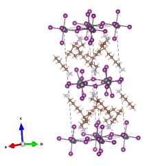
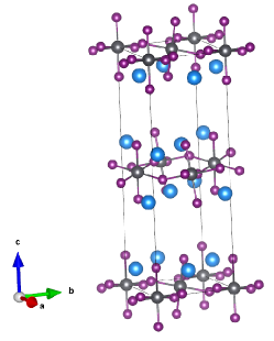
Fig. 2 illustrates the crystal structure of the low-temperature structure[23] of (BA)2PbI4 layered material. There are PbI4 perovskite layers which are intercalated by butylammonium chains. Notice that the atomic positions in two successive PbI4 perovskite layers are staggered relative to the atomic positions of the same atoms in their nearest neighboring layer. As a result the unit-cell of the Bravais lattice is twice as long along the axis.
II.2 (BA)2PbI4 Band Structure
First, we carried out calculations for the (BA)2PbI4 structure[19] shown in the left panel of Fig. 2 using the Quantum Espresso[24] (QE) implementation of the density functional theory (DFT) in the GGA framework. The Perdew-Burke-Ernzerhof (PBE) exchange correlation functional[25] was used with Projector Augmented-Wave [26] pseudopotentials generated with a scalar-relativistic calculation local potential using the “atomic” code by Dal Corso[27]. Our self-consistently converged ground-state calculation used a k-point mesh and a 30 Rd energy cut-off. In Appendix A a convergence study demonstrates that the k-point mesh and the energy cut-off used are accurate for the purpose of the present paper.
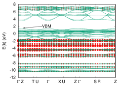
Our first objective is to establish that the atomic orbitals of the butylammonium organic ligands, i.e., the orbitals of C, N and H, have negligible contribution to the Bloch states with energy which falls in the energy window of 1 eV below the top of the VBM and 2 eV above the CBM, which, including the gap is about a 5 eV range. Fig. 3 illustrates that there is insignificant projection of each of the Bloch states to the local orbitals of all C, N and H.
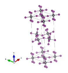
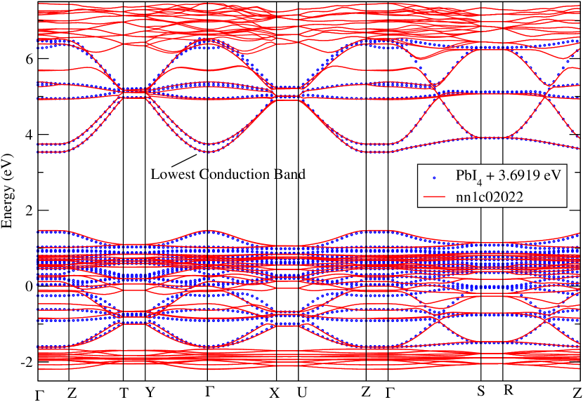
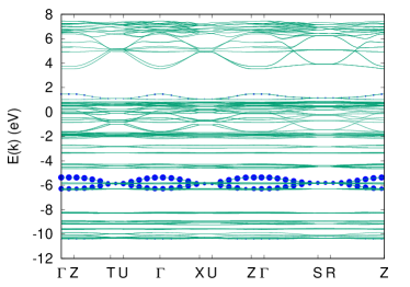
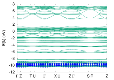
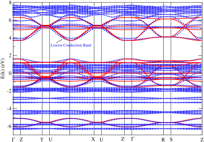
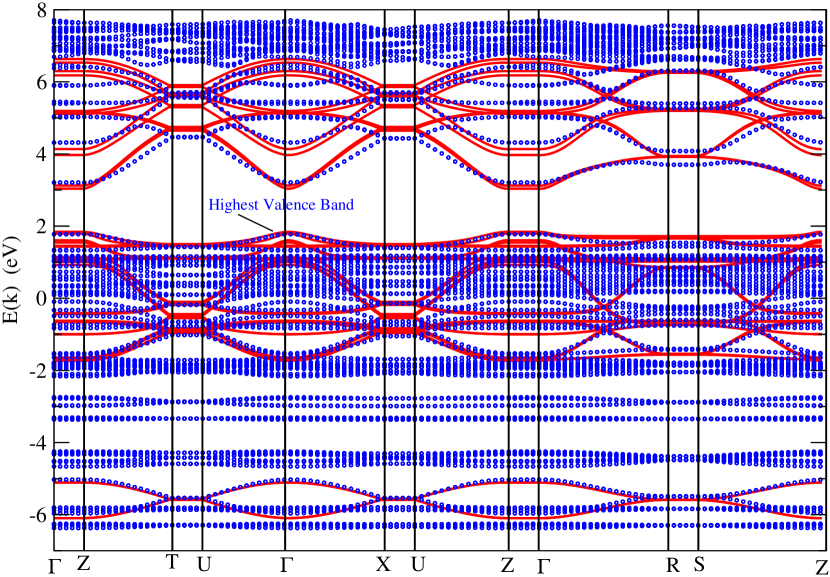
Using the same exchange correlation functional and pseudopotentials as in the case of (BA)2PbI4, we carried out a self-consistent-field (SCF) DFT ground state calculation for the “bare-bone” perovskite atomic matrix illustrated in the middle panel of Fig. 2, i.e., without the intercalating butylammonium chains. We then computed the bands along the same crystallographic directions as for the (BA)2PbI4 for comparison. These bands are shown in Fig. 4 as blue circles and are compared with those of the complete material (BA)2PbI4 (shown as red-lines).
Notice that the agreement between the bands near the Fermi level is very good. The position of the Fermi level is different for the real material (BA)2PbI4 as compared to the simple PbI4 matrix because the intercalating butylammonium chains add more electrons to these bands, thus, raising the Fermi level and making it a band insulator. The important conclusion is that the bands near the Fermi level and their Bloch wavefunctions, assuming the same atomic positions, are determined by the PbI4 matrix to a good degree of accuracy.
II.3 Projecting Bloch states near the Fermi energy to atomic orbitals
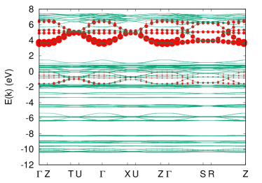
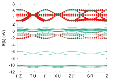
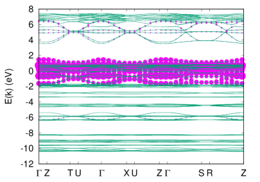
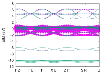
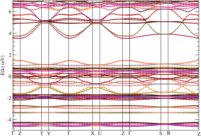
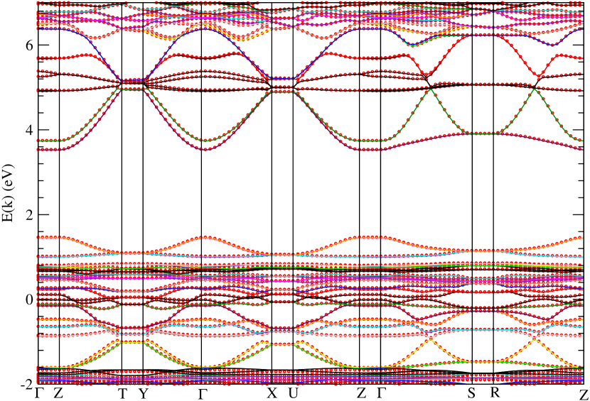
Next, we wish to determine the orbital character of the bands inside the energy window of our interest. Since we have demonstrated in the previous section that these bands are almost completely determined by the Pb and I atoms we projected the bands in the orbitals of those atoms only. In Figs. 5,6 the projection of the bands in the atomic orbitals are shown. The size of the circle is proposal to the contribution of the particular orbital to the given band. The orbitals chosen are those that contribute to the bands and lie within eV from the Fermi level. These are the Pb outer orbitals, i.e., 6, and and the I and . Notice that the projections for the case of (BA)2PbI4 (left panels), and those of the PbI4 halide-perovskite “matrix” (right panels) are very similar. In addition, we note that top valence bands and the lower conduction bands (i.e., with band energy less than about 5 eV and above 0 eV) are mostly made out of (Pb or I) orbitals. There is a very small amount of orbital contribution.
II.4 Removing the organic molecules and adding Cs at the location of N sites: Cs2PbI4
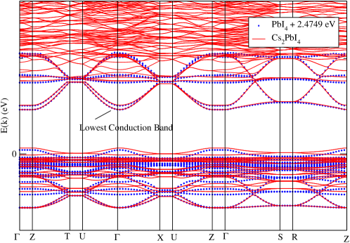
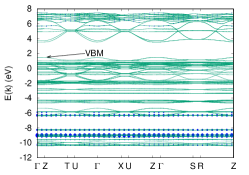
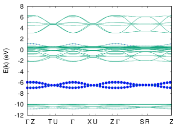
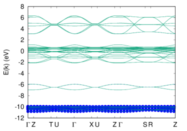
In order to clearly demonstrate the almost irrelevance of the butylammonium chains on the band-structure near the Fermi level, we calculated the band-structure of the a compound obtained by removing all the butylammonium chains and by adding Cs at the N sites of the original (BA)2PbI4 compound. We choose Cs based on its electronegativity relative to the Fermi level of the PbI4 matrix, in order to make sure that the energy level of the outer Cs level falls above the energy of the highest occupied band, such that these Cs states will be empty inside the compound, thus, resulting in doping the PbI4 matrix in the same manner as the alkylammonium chains cause doping. The structure is illustrated in the left panel of Fig 7 and the DFT calculated band structure is compared to the (BA)2PbI4 compound in right panel of Fig. 7.
This compound exists in nature but with different lattice constants than those used in this calculation: we wish to keep them the same as in the (BA)2PbI4 for direct comparison of the bands. Notice that after shifting the energy of all the bands of PbI4 by the same amount of 2.4749 eV there is very good agreement between the bands near the Fermi energy. This finding strengthens our conclusion and makes transparent our statement that the bands of the PbI4 matrix almost solely determine the band structure within 1 eV below the VBM and 2 eV above the bottom of the CBM, which, including the energy gap, is about a 5 eV energy range.
III Tight-binding model
From the previous comparison we conclude that it makes sense to derive a TB model to describe these rigid-band features. In this model the role of all the interlayer butylammonium chains is to create the structure, and their role in the electronic structure is to provide one additional electron per Pb atom. Therefore, in our TB model which aims at describing these rigid band features for only the bands in the energy window of our interest discussed previously, the intercalating organic chains will be ignored.
We start from a symmetric system without any octahedra distortions and we choose the -axis and axis to be of the same length, i.e., the lattice has the symmetry of the square-lattice. In the real material the and axes are very close to each other, namely, .
First, we ignore the interplane coupling, which reduces the effective unit-cell to one with half the number of atoms. Notice that the bands obtained by the DFT calculation have different bandwidths along the axis. The bands that are mostly made of Hydrogen atomic orbitals, i.e., from the butylammonium chains have significant bandwidth of the order of 0.1 eV. The bands of our interest, however, i.e., those within the region of 5 eV near the Fermi level, have remarkably negligible dispersion along the axis. The bandwidth of these bands is less than 0.01 eV. This justifies our treatment of these bands as two-dimensional.
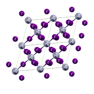
In addition, as a first step, we are going to ignore the role of the I atoms which are off the plane which reduces the problem to the 2D unit-cell shown on the left panel of Fig. 8. We will also discuss how to include these off-planar atoms displayed on the right panel of Fig. 8 as a second stage.
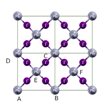
Next, we are going to consider matrix elements of the Hamiltonian between the following twelve (12) states inside the unit-cell of the reduced Bravais lattice: , and , where for the 3 atoms in the reduced unit cell, i.e., the Pb atom at the origin , the I atom at and the I atom at . We note that throughout the rest of the paper, our and axes are with respect to the rotated coordinate system, not the original unit cell. The state for is the Pb orbital and for it is the I orbital. The states and where corresponds to the Pb orbitals, whereas when it corresponds to the I orbitals.
Matrix elements of the form when are the on-site energies, which are , , while off-diagonal matrix elements are non-zero only if the atoms are nearest neighbors, in which case they are .
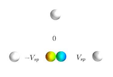
Matrix elements between a orbital of a Pb atom and a -type orbital of any of its nearest neighbor I atoms or vice-versa, when non-zero, are given by or . Because of the negative eigenvalue of the orbital with respect to reflections about a plane perpendicular to the -axis, some of these matrix elements are zero and others have a relative minus sign as illustrated in the left panel of Fig. 9.
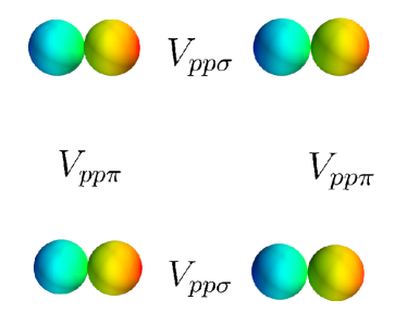
There two kinds of matrix elements of between the same type of -orbitals as illustrated in the right panel of Fig. 9. As explained in the figure caption of this figure, they can be either of -type, i.e., or of -type, i.e., . One has to be careful about their relative sign and when these matrix elements are zero.
| 0 | 0 | 0 | 0 | 0 | 0 | 0 | ||||||
| 0 | 0 | 0 | 0 | 0 | 0 | 0 | 0 | |||||
| 0 | 0 | 0 | 0 | 0 | 0 | 0 | 0 | |||||
| 0 | 0 | 0 | 0 | 0 | 0 | 0 | 0 | 0 | ||||
| 0 | 0 | 0 | 0 | 0 | 0 | 0 | 0 | 0 | ||||
| - | 0 | 0 | 0 | 0 | 0 | 0 | 0 | 0 | 0 | |||
| 0 | 0 | 0 | 0 | 0 | 0 | 0 | 0 | 0 | 0 | |||
| 0 | 0 | 0 | 0 | 0 | 0 | 0 | 0 | 0 | 0 | |||
| 0 | 0 | 0 | 0 | 0 | 0 | 0 | 0 | 0 | ||||
| 0 | 0 | 0 | 0 | 0 | 0 | 0 | 0 | 0 | 0 | |||
| 0 | 0 | 0 | 0 | 0 | 0 | 0 | 0 | 0 | ||||
| 0 | 0 | 0 | 0 | 0 | 0 | 0 | 0 | 0 | 0 |
| -9.3 | -0.2 | -0.2 | -13.05 | -2.8 | -3.0 | -2.5 | 0.8 | 1.2 | -0.6 | 0.8 |
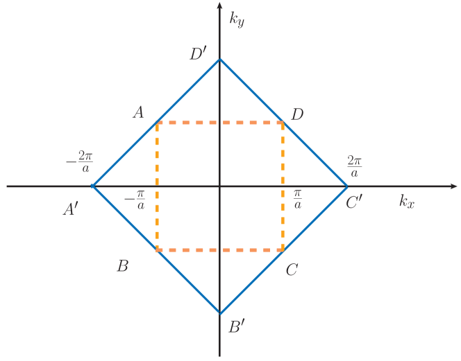
First, instead of using the unit-cell illustrated in the left panel of Fig. 8 by the ABCD square, which is the one that is necessary to use when the symmetry is broken by the octahedra tilting, we use as unit-cell the smaller size square EBFC which is rotated by with respect to the original. This unit-cell contains only one Pb and two I atoms and, therefore, 12 states. This doubles the size of the BZ from the orange square of Fig. 10 to the square labeled , which is rotated by with respect to the x-axis. Therefore, for our convenience, we will solve the problem in this larger BZ (where we have only 12 states for each ) and in order to compare with the results of the original BZ, we will need to fold this BZ to the smaller size one. This folding will increase the number of bands by a factor of two and, therefore, we will be able to recover the total number of 24 bands, which were present in the original unit-cell of the Bravais lattice.
If we include the matrix elements illustrated in Fig. 9 and we transform our Hamiltonian in momentum space, the Hamiltonian matrix becomes momentum-diagonal i.e.,
| (1) |
where the sum is over the entire Brillouin zone (blue square of Fig 10) and is a matrix given in Table 1, where
| (2) | |||||
| (3) |
The subscripts and in the above -dependent coefficients are labeled according to our and axes which are with respect to the rotated coordinate system, not the original unit cell. The and , however, are the and projections of on the corresponding and axes of the original un-rotated unit-cell. We use the latter for making comparison with the bands obtained by DFT.
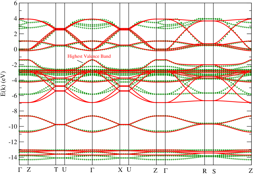
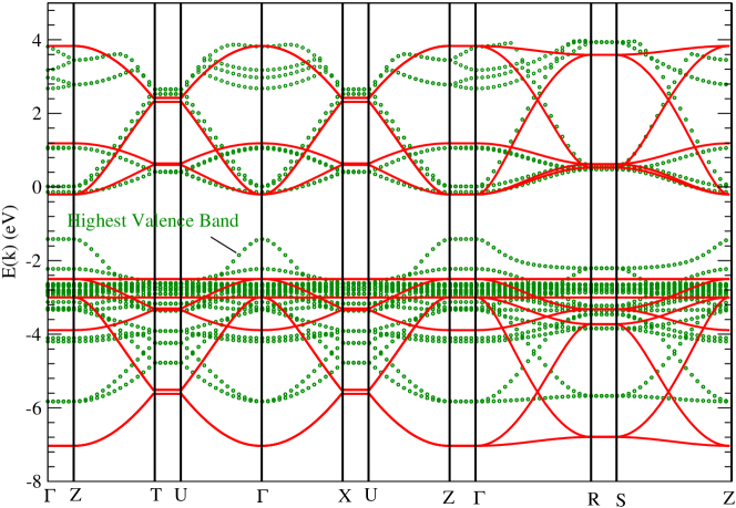
A numerical diagonalization of the above at every -point leads to the results illustrated in Fig. 11 which are compared to the results of the DFT of a 3D PbI4 crystal without octahedral distortions and with . The results of the fitting parameters is given in Table 2. We note that the disagreement for the highest energy bands is due to the fact that these bands are at positive (unbound) energy and, therefore, the DFT calculation has included the effects of unbound electronic states. The DFT calculation involves more states because it includes the off-plane I atoms (see structure illustrated in the right panel of Fig. 8). The TB matrix (a matrix) which includes the and orbital of these atoms is given in Appendix B. There are several more fitting parameters to use in this case and the agreement can be improved by introducing some of the missing bands away from the Fermi level. Such an approach, however, would lead to significant complication which works against our goal of simplifying the problem and leaving the description near the Fermi energy as accurate as possible. We have implemented this more complex TB Hamiltonian but the fact that it yields 16 additional bands (when we fold the BZ) leads to a fitting procedure which does not have a unique and simple solution. For completeness, however, we provide this more complex TB Hamiltonian matrix in the Table of Appendix B and we leave out from this paper the ambiguous results of such a fit.
In Sec. IV.3 we will use our TB model to fit the results of the actual 3D (BA)2PbI4 crystal, where we find that the quality of the fit is equally good. First, however, we would like to discuss an analytical treatment of the problem, which we do in the next Section.
IV Analytical description
Here, we describe a simplified analytical treatment of the problem which contains all the essential elements of the original system near the Fermi level.
IV.1 Non-interacting and orbitals
First, we define the model subspace, which is all the orbitals that fall inside the energy range of our interest which is 1 eV below the VBM and 2 eV above the CBM. These states are the Pb and the I orbitals. The Hamiltonian acting inside this model subspace is the following:
| (4) |
where corresponds to the orbital , i.e., the Pb orbital, i.e.,
| (5) |
and
| (9) |
in the basis where 1,2,3 stand for the Pb and the two () orbitals of its neighboring I atoms. Here
| (10) | |||||
| (11) | |||||
| (12) |
Next, we will include the coupling of this subspace to the states which are outside this energy range but not too far away. For example, we will include the coupling between the Pb and the I because the latter falls inside the subspace of our interest, but we will ignore the coupling between Pb and the I state as the latter state is too far below ( eV) the VBM and is only 0.8 eV, namely, . We will consider as this couples the Pb and I orbitals which are far from the above energy range and both states fall outside the energy domain of our interest. The resulting Hamiltonian is given by
| (13) |
The couples the Pb (i.e., ) with and .
| (17) |
Diagonalization of the matrices , , , of the model subspace yields the following eigenvalues:
| (18) | |||||
| (19) |
The corresponding eigenstates for each of the above cases are given by the following form:
| (20) | |||||
| (21) | |||||
| (22) | |||||
| (23) |
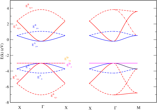
The unit-cell doubling and rotation leads to the folding of the BZ which doubles the number of eigenvalues to 18 (some of which are degenerate in this higher symmetry Hamiltonian). They are illustrated in Fig. 12 and are compared to the DFT calculation in Fig. 13 using the same values of the parameters of Table 2 but ignoring the orbitals completely, i.e., . Notice that the occupied bands are described well, notice, however, that the top of the valence band (i.e., the I state) is flat and the model does not describe its dispersion. The main reason for this discrepancy is its coupling to the Pb and it is corrected in the next subsection.
IV.2 Integrating out the Pb orbitals
The I bands or are flat in this approximation. Next we include the role of the Pb and I hybridization which will account for the dispersion of the top valence band (which corresponds to the flat band illustrated by the green-line in Fig. 12. The hybridization of the Pb orbital with the I , i.e., the matrix element , couples the and the and as in Eq. 17.
This interaction is crucial when there is an exact or almost degeneracy at specific points between the and bands given by Eq. 19. This happens at the point for the four bands and when they are folded at . If we include the state this becomes a matrix, which cannot be analytically diagonalized. However, because the state is well below the Fermi level such that , we can apply perturbation theory in . More precisely, we will apply quasi-degenerate stationary perturbation theory[28] to integrate out the orbital in second order. Using Eq. 23 for the eigenstates, the second-order-corrected diagonal matrix-elements (i.e., which include the effect of the virtual transition from the state to state and back) are given as follows:
| (24) | |||||
| (25) | |||||
| (26) | |||||
| (27) |
The off-diagonal matrix elements vanish along the high-symmetry directions in our plot of Fig. 14. Along other directions, the off-diagonal elements do not necessarily vanish. In this case we would need to diagonalize the matrix. However, this cannot be done analytically, and if we need to resort to a numerical diagonalization we might as well diagonalize the full matrix to obtain the more exact non-perturbative solution. The purpose of this subsection was to demonstrate that the origin of the dispersion of the upper valence band is from the coupling which, we feel, has been achieved.
IV.3 Fitting the full crystal with the same tight-binding model
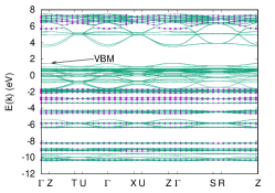
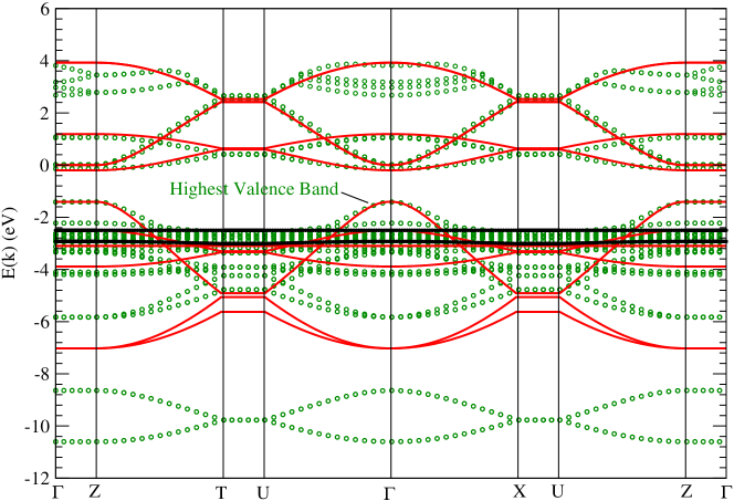
Now that we have an analytical understanding of the origin of the band character near the Fermi level, we can proceed and modify the parameters of our TB model (Table 1) listed in Table 2 in order to provide a good fit of the material of our focus, i.e., (BA)2PbI4.
The result of the fit is illustrated in Fig. 15 and the values of the parameters that produce this TB fit are given in Table 3.
| -6.0 | -3.3 | -4.9 | -10.0 | 1.1 | -0.5 | -1.8 | 0.5 | 1.8 | 0.6 | 0.8 |
We notice that the TB model describes very well all the bands which are due to the orbitals in PbI4. However, these orbitals are the only ones that have non-negligible contribution to the bands in the energy range of out interest, which is discussed in the abstract.
V Spin-orbit coupling
Once we have established our TB model, it is straightforward to include the contribution of spin-orbit-coupling (SOC). The orbitals of Pb and the orbital of the two I atoms in the unit cell give no contribution. The non-zero contribution comes from the Pb orbital and the orbital of the two I atoms (atoms 2 and 3 in our unit-cell). We need to add the following part to the TB Hamiltonian and carry out the diagonalization in a space of double dimension.
| (28) |
where (and ) is the SOC of the Pb (and of the I ) orbital with the electron spin. Each of the three terms above in the basis , , , , , , for is given in Table 4 in units of ( , , ).
| 0 | - | 0 | 0 | 0 | 1 | |
| 0 | 0 | 0 | 0 | - | ||
| 0 | 0 | 0 | -1 | 0 | ||
| 0 | 0 | -1 | 0 | 0 | ||
| 0 | 0 | - | - | 0 | 0 | |
| 1 | 0 | 0 | 0 | 0 |
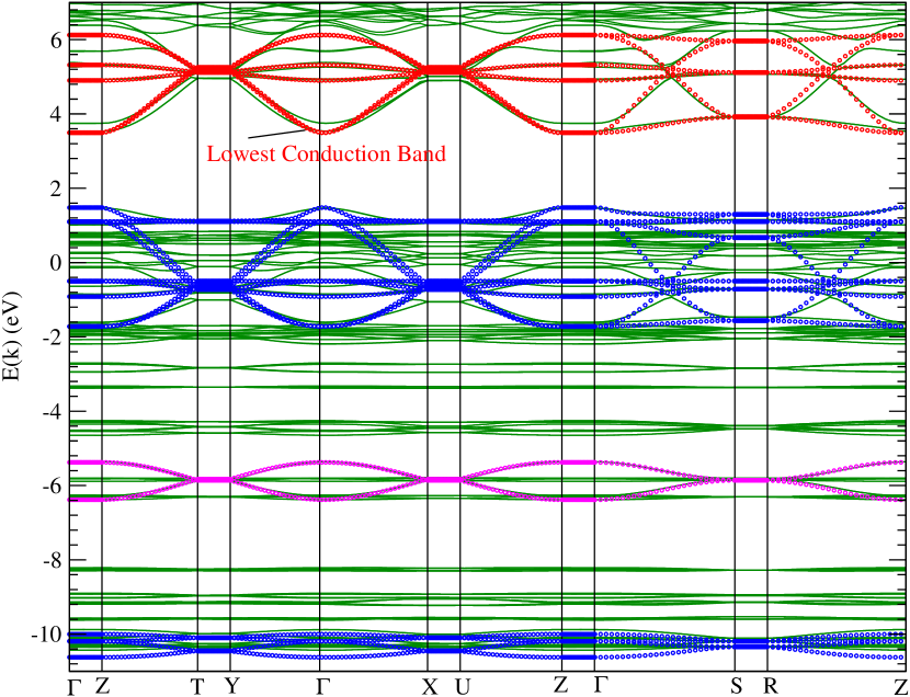
In order to add the SOC in the DFT calculation we need fully relativistic pseudopotentials (FRP) and we will utilize those provided in Ref. [29]. First, we carry out a SCF calculation on the same size k-point mesh as in our previous calculations and the highest energy-cutoff suggested in the pseudopotential files. In Fig. 16 we illustrate that our TB model fits with the same level of accuracy the results using these FRP without SOC. We need this step in order to carry out the fit of the calculation with SOC. We note that the values of the TB parameters are only slightly off using this FRP. Next, without changing any of these TB parameters, we simply add the SOC Hamiltonian described in the previous paragraph and we fit the results by using only the two fitting parameters and . The results are shown in Fig. 17. The effect of the SOC coupling is large as expected for Pb and I, however, we also know from previous work that DFT tends to overestimate the effects of the SOC (see related discussion in Refs. [30, 31]). However, the goal of the present paper is to provide a reasonable starting one-electron model Hamiltonian without the inclusion of SOC and other effects, such as the effects of correlations. As discussed, the model can be the starting point for calculations to include these effects more accurately. For example, the effect of the SOC could be more accurately included by fitting the value of the SOC (using the above model independent form) to the results of a quasiparticle-self-consistent GW calculation[32] or to the experimental results for the gap or other experimentally determined parameters.
The simple calculation presented above demonstrates the value of the present paper where the TB and the effective models were determined. Namely, without changing the parameters of the TB Hamiltonian, i.e., using their values determined without the inclusion of the SOC, we were able to accurately include the effects of the SOC by simply adding the SOC to our model. Similarly, other effects, such as the effects of correlations, the Jahn-Teller effect, optical response, etc, can be included starting from the present model.
VI Other terms
There are other important physical effects which yield corrections to the above treatment, such as the octahedra distortions.
The octahedral distortions break the C4 symmetry and that folds the BZ back to its observed form. In addition, they open gaps at high-symmetry points and lift band-degeneracies along high-symmetry directions.
Depending on the problem at hand to address, these terms can be important to include, which can be added on top the TB Hamiltonian considered in the present work. There are problems, however, where the TB-treatment of the present paper can be a good starting point. For example, and this is one of our future projects, starting from this TB-model we can include the role of electron interactions to study exciton bound-states. These involve bound-states of electron/hole pairs excited from near the VBM to near the CBM where the TB description is reasonably good.
The goal of the present paper was to provide an as simple as possible and yet accurate analytic and semianalytic description of the complex band-structure of the simplest member of the series of the 2D halide-perovskite materials. Future work should extend this treatment to members of this family and should include the role of the above smaller effects. Another direction should be to include the role of electron interactions in many-body phenomena, such as the role of excitons in these systems.
VII Discussion and summary
Simplifying the very complex band-structure of the 2D Ruddlesden-Popper perovskite materials and providing a simple model which accurately reproduces its main features and, which quantitatively describes it, is the main goal of the present paper. Such a simplified picture, not only allows us to grasp the physics of the electronic structure of these materials, which might help our thinking forward, but it can also provide a simple description of the one-body part of an effective many-body Hamiltonian to use to carry out many-body calculations.
First, we have illustrated that, in the simplest case of the series (BA)2(MA)m-1PbmI3m+1 with m=1, i.e., for (BA)2PbI4, the bands in the energy range: 1 eV below the VBM to 2 eV above the CBM, a 5 eV range covering the range of the photo-electric response, have negligible contribution from the atomic orbitals contained in the BA ligands. This conclusion is not to diminish the significance of organic chains in general. As an example of their significance, we would like to mention that the small organic chains, such as the MA, (which are absent in the m=1 case) reduce dielectric screening within a monolayer of RP perovskite materials, which helps generate stable excitons at room temperature with binding energies of the order of hundreds of meV[6, 33, 34]. In addition, their physical properties are influenced by the number of layers that affects the exciton binding energy. However, in the m=1 case, the role of the atoms of these BA chains is solely to stabilize the structure and to act as a charge reservoir which fills completely the highest occupied bands making the material an insulator. We demonstrate that other materials, which share the same halide-perovskite core matrix or even just the “matrix” formed by the same halide-perovskite layer, (keeping the structure and all the atomic distances the same) have very similar band-structure in the above defined energy range.
Further, we analyzed the complex band-structure of this class of materials for m=1 and found a simple 2D TB model which can accurately reproduce the band-structure as obtained by DFT in the above energy window. We were also able to simplify this TB model in such a way that it allows an analytical, transparent and accurate way to describe the origin of all the features of the band-structure. As a consequence, a simple band-picture emerges out of the complexity of the bands as obtained by straightforward application of DFT. By considering a two-dimensional TB model, which ignores the small octahedra distortions, it allows us to reduce the size of the unit-cell by a factor of two, a fact that doubles the Brillouin-zone by unfolding it because of symmetry. This reduces the TB Hamiltonian to a smaller matrix. The most important conduction and relevant conduction and valence bands are obtained as a hybridization of mostly Pb and I orbitals in the case of our example (BA)2PbI4. To obtain the correct dispersion of the highest valence-band, we also needed to involve the role of the hybridization between the Pb orbital and the orbital of the I atoms that form the octahedra corners. Finally, we offer a simple analytic description of the band-structure by integrating out this Pb orbital as it sits energetically well below the above mentioned energy range.
As already discussed in the previous section, there are several directions where the results of the present work can be useful and also ways in which other effects can be incorporated depending on the problem at hand. For example, the simple TB model uncovered in this paper will be useful in carrying out many-body calculations to describe excitonic properties of these materials[35] which is our future goal.
VIII Acknowledgment
I would like to thank Hanwei Gao for useful interactions. This work was supported by the U.S. National Science Foundation under Grant No. NSF-EPM-2110814.
Appendix A DFT convergence study
Our self-consistently converged ground-state calculation used a and a k-point-mesh size. The results are compared in Fig. 18 and we conclude that the size is large enough for the purpose of the present paper. In Fig. 19 we compare the results of our DFT calculation for size for energy cutoff of 30 Rd (red circles) and 40 Rd (solid lines) to show that using 30 Rd as the energy cutoff is large enough for the purpose of the present paper.
Appendix B More complex tight-binding matrix
Generalization of our TB model of Table 1 for the model complete 2d-halide-perovskite illustrated in the right panel of Fig. 8 leads to the TB matrix given in Table 5. This model includes the pair of I atoms per Pb atom which are off the plane and complete the octahedra.
| 0 | 0 | 0 | 0 | 0 | 0 | 0 | 0 | 0 | 0 | 0 | ||||||||||
| 0 | 0 | 0 | 0 | 0 | 0 | 0 | 0 | 0 | 0 | 0 | 0 | 0 | 0 | |||||||
| 0 | 0 | 0 | 0 | 0 | 0 | 0 | 0 | 0 | 0 | 0 | 0 | 0 | 0 | |||||||
| 0 | 0 | 0 | 0 | 0 | 0 | 0 | 0 | 0 | - | 0 | 0 | - | 0 | 0 | ||||||
| 0 | 0 | 0 | 0 | 0 | 0 | 0 | 0 | 0 | 0 | 0 | 0 | 0 | 0 | 0 | 0 | 0 | ||||
| - | 0 | 0 | 0 | 0 | 0 | 0 | 0 | 0 | 0 | 0 | 0 | 0 | 0 | 0 | 0 | 0 | 0 | |||
| 0 | 0 | 0 | 0 | 0 | 0 | 0 | 0 | 0 | 0 | 0 | 0 | 0 | 0 | 0 | 0 | 0 | 0 | |||
| 0 | 0 | 0 | 0 | 0 | 0 | 0 | 0 | 0 | 0 | 0 | 0 | 0 | 0 | 0 | 0 | 0 | 0 | |||
| 0 | 0 | 0 | 0 | 0 | 0 | 0 | 0 | 0 | 0 | 0 | 0 | 0 | 0 | 0 | 0 | 0 | ||||
| 0 | 0 | 0 | 0 | 0 | 0 | 0 | 0 | 0 | 0 | 0 | 0 | 0 | 0 | 0 | 0 | 0 | 0 | |||
| 0 | 0 | 0 | 0 | 0 | 0 | 0 | 0 | 0 | 0 | 0 | 0 | 0 | 0 | 0 | 0 | 0 | ||||
| 0 | 0 | 0 | 0 | 0 | 0 | 0 | 0 | 0 | 0 | 0 | 0 | 0 | 0 | 0 | 0 | 0 | 0 | |||
| 0 | 0 | 0 | 0 | 0 | 0 | 0 | 0 | 0 | 0 | 0 | 0 | 0 | 0 | 0 | 0 | 0 | ||||
| 0 | 0 | 0 | 0 | 0 | 0 | 0 | 0 | 0 | 0 | 0 | 0 | 0 | 0 | 0 | 0 | 0 | 0 | |||
| 0 | 0 | 0 | 0 | 0 | 0 | 0 | 0 | 0 | 0 | 0 | 0 | 0 | 0 | 0 | 0 | 0 | 0 | |||
| - | 0 | 0 | 0 | 0 | 0 | 0 | 0 | 0 | 0 | 0 | 0 | 0 | 0 | 0 | 0 | 0 | 0 | |||
| 0 | 0 | 0 | 0 | 0 | 0 | 0 | 0 | 0 | 0 | 0 | 0 | 0 | 0 | 0 | 0 | 0 | ||||
| 0 | 0 | 0 | 0 | 0 | 0 | 0 | 0 | 0 | 0 | 0 | 0 | 0 | 0 | 0 | 0 | 0 | 0 | |||
| 0 | 0 | 0 | 0 | 0 | 0 | 0 | 0 | 0 | 0 | 0 | 0 | 0 | 0 | 0 | 0 | 0 | 0 | |||
| - | 0 | 0 | 0 | 0 | 0 | 0 | 0 | 0 | 0 | 0 | 0 | 0 | 0 | 0 | 0 | 0 | 0 |
References
- Stoumpos et al. [2016] C. C. Stoumpos, D. H. Cao, D. J. Clark, J. Young, J. M. Rondinelli, J. I. Jang, J. T. Hupp, and M. G. Kanatzidis, Ruddlesden–popper hybrid lead iodide perovskite 2d homologous semiconductors, Chemistry of Materials 28, 2852 (2016).
- Mitzi [1996] D. B. Mitzi, Synthesis, crystal structure, and optical and thermal properties of (c4h9nh3)2mi4 (m = ge, sn, pb), Chemistry of Materials 8, 791 (1996).
- Ruddlesden and Popper [1958] S. N. Ruddlesden and P. Popper, The compound sr3ti2o7and its structure, Acta Crystallographica 11, 54 (1958).
- Gao et al. [2019] Y. Gao, E. Shi, S. Deng, S. B. Shiring, J. M. Snaider, C. Liang, B. Yuan, R. Song, S. M. Janke, A. Liebman-Peláez, P. Yoo, M. Zeller, B. W. Boudouris, P. Liao, C. Zhu, V. Blum, Y. Yu, B. M. Savoie, L. Huang, and L. Dou, Molecular engineering of organic–inorganic hybrid perovskites quantum wells, Nature Chemistry 11, 1151 (2019).
- Dou et al. [2015] L. Dou, A. B. Wong, Y. Yu, M. Lai, N. Kornienko, S. W. Eaton, A. Fu, C. G. Bischak, J. Ma, T. Ding, N. S. Ginsberg, L.-W. Wang, A. P. Alivisatos, and P. Yang, Atomically thin two-dimensional organic-inorganic hybrid perovskites, Science 349, 1518 (2015), https://www.science.org/doi/pdf/10.1126/science.aac7660 .
- Blancon et al. [2020] J.-C. Blancon, J. Even, C. C. Stoumpos, M. G. Kanatzidis, and A. D. Mohite, Semiconductor physics of organic–inorganic 2d halide perovskites, Nature Nanotechnology 15, 969 (2020).
- Manser et al. [2016] J. S. Manser, J. A. Christians, and P. V. Kamat, Intriguing optoelectronic properties of metal halide perovskites, Chemical Reviews 116, 12956 (2016).
- Thirumal et al. [2017] K. Thirumal, W. K. Chong, W. Xie, R. Ganguly, S. K. Muduli, M. Sherburne, M. Asta, S. Mhaisalkar, T. C. Sum, H. S. Soo, and N. Mathews, Morphology-independent stable white-light emission from self-assembled two-dimensional perovskites driven by strong exciton–phonon coupling to the organic framework, Chemistry of Materials 29, 3947 (2017).
- Bellani et al. [2021] S. Bellani, A. Bartolotta, A. Agresti, G. Calogero, G. Grancini, A. Di Carlo, E. Kymakis, and F. Bonaccorso, Solution-processed two-dimensional materials for next-generation photovoltaics, Chem. Soc. Rev. 50, 11870 (2021).
- Sun et al. [2021] S. Sun, M. Lu, X. Gao, Z. Shi, X. Bai, W. W. Yu, and Y. Zhang, 0d perovskites: Unique properties, synthesis, and their applications, Advanced Science 8, 2102689 (2021), https://onlinelibrary.wiley.com/doi/pdf/10.1002/advs.202102689 .
- Ban et al. [2018] M. Ban, Y. Zou, J. P. H. Rivett, Y. Yang, T. H. Thomas, Y. Tan, T. Song, X. Gao, D. Credgington, F. Deschler, H. Sirringhaus, and B. Sun, Solution-processed perovskite light emitting diodes with efficiency exceeding 15% through additive-controlled nanostructure tailoring, Nature Communications 9, 3892 (2018).
- Zhang et al. [2021] L. Zhang, C. Sun, T. He, Y. Jiang, J. Wei, Y. Huang, and M. Yuan, High-performance quasi-2d perovskite light-emitting diodes: from materials to devices, Light: Science & Applications 10, 61 (2021).
- Schmidt-Mende et al. [2021] L. Schmidt-Mende, V. Dyakonov, S. Olthof, F. Ünlü, K. M. T. Lê, S. Mathur, A. D. Karabanov, D. C. Lupascu, L. M. Herz, A. Hinderhofer, F. Schreiber, A. Chernikov, D. A. Egger, O. Shargaieva, C. Cocchi, E. Unger, M. Saliba, M. M. Byranvand, M. Kroll, F. Nehm, K. Leo, A. Redinger, J. Höcker, T. Kirchartz, J. Warby, E. Gutierrez-Partida, D. Neher, M. Stolterfoht, U. Würfel, M. Unmüssig, J. Herterich, C. Baretzky, J. Mohanraj, M. Thelakkat, C. Maheu, W. Jaegermann, T. Mayer, J. Rieger, T. Fauster, D. Niesner, F. Yang, S. Albrecht, T. Riedl, A. Fakharuddin, M. Vasilopoulou, Y. Vaynzof, D. Moia, J. Maier, M. Franckevičius, V. Gulbinas, R. A. Kerner, L. Zhao, B. P. Rand, N. Glück, T. Bein, F. Matteocci, L. A. Castriotta, A. Di Carlo, M. Scheffler, and C. Draxl, Roadmap on organic–inorganic hybrid perovskite semiconductors and devices, APL Materials 9, 109202 (2021), https://doi.org/10.1063/5.0047616 .
- Catone et al. [2021] D. Catone, G. Ammirati, P. O’Keeffe, F. Martelli, L. Di Mario, S. Turchini, A. Paladini, F. Toschi, A. Agresti, S. Pescetelli, and A. Di Carlo, Effects of crystal morphology on the hot-carrier dynamics in mixed-cation hybrid lead halide perovskites, Energies 14, 10.3390/en14030708 (2021).
- Milot et al. [2016] R. L. Milot, R. J. Sutton, G. E. Eperon, A. A. Haghighirad, J. Martinez Hardigree, L. Miranda, H. J. Snaith, M. B. Johnston, and L. M. Herz, Charge-carrier dynamics in 2d hybrid metal–halide perovskites, Nano Letters 16, 7001 (2016).
- Cho et al. [2020] J. Cho, J. T. DuBose, and P. V. Kamat, Charge carrier recombination dynamics of two-dimensional lead halide perovskites, The Journal of Physical Chemistry Letters 11, 2570 (2020).
- Gan et al. [2019] Z. Gan, X. Wen, C. Zhou, W. Chen, F. Zheng, S. Yang, J. A. Davis, P. C. Tapping, T. W. Kee, H. Zhang, and B. Jia, Transient energy reservoir in 2d perovskites, Advanced Optical Materials 7, 1900971 (2019), https://onlinelibrary.wiley.com/doi/pdf/10.1002/adom.201900971 .
- Wu et al. [2015] X. Wu, M. T. Trinh, and X.-Y. Zhu, Excitonic many-body interactions in two-dimensional lead iodide perovskite quantum wells, The Journal of Physical Chemistry C 119, 14714 (2015).
- Umebayashi et al. [2003] T. Umebayashi, K. Asai, T. Kondo, and A. Nakao, Electronic structures of lead iodide based low-dimensional crystals, Phys. Rev. B 67, 155405 (2003).
- Wu et al. [2021] G. Wu, T. Yang, X. Li, N. Ahmad, X. Zhang, S. Yue, J. Zhou, Y. Li, H. Wang, X. Shi, S. F. Liu, K. Zhao, H. Zhou, and Y. Zhang, Molecular engineering for two-dimensional perovskites with photovoltaic efficiency exceeding 18, Matter 4, 582 (2021).
- Cao et al. [2022] Q. Cao, P. Li, W. Chen, S. Zang, L. Han, Y. Zhang, and Y. Song, Two-dimensional perovskites: Impacts of species, components, and properties of organic spacers on solar cells, Nano Today 43, 101394 (2022).
- Chen et al. [2018] A. Z. Chen, M. Shiu, J. H. Ma, M. R. Alpert, D. Zhang, B. J. Foley, D.-M. Smilgies, S.-H. Lee, and J. J. Choi, Origin of vertical orientation in two-dimensional metal halide perovskites and its effect on photovoltaic performance, Nature Communications 9, 1336 (2018).
- Menahem et al. [2021] M. Menahem, Z. Dai, S. Aharon, R. Sharma, M. Asher, Y. Diskin-Posner, R. Korobko, A. M. Rappe, and O. Yaffe, Strongly anharmonic octahedral tilting in two-dimensional hybrid halide perovskites, ACS Nano 15, 10153 (2021).
- Giannozzi et al. [2009] P. Giannozzi, S. Baroni, and N. B. et al, Quantum espresso: a modular and open-source software project for quantum simulations of materials, Journal of Physics: Condensed Matter 21, 395502 (2009).
- Perdew et al. [1996] J. P. Perdew, K. Burke, and M. Ernzerhof, Generalized gradient approximation made simple, Phys. Rev. Lett. 77, 3865 (1996).
- Kresse and Joubert [1999] G. Kresse and D. Joubert, From ultrasoft pseudopotentials to the projector augmented-wave method, Phys. Rev. B 59, 1758 (1999).
- Dal Corso [2010] A. Dal Corso, Projector augmented-wave method: Application to relativistic spin-density functional theory, Phys. Rev. B 82, 075116 (2010).
- Manousakis [2016] E. Manousakis, Practical Quantum Mechanics (Oxford University Press, 2016).
- Hamann [2013] D. R. Hamann, Optimized norm-conserving vanderbilt pseudopotentials, Phys. Rev. B 88, 085117 (2013).
- Rhodes et al. [2017] D. Rhodes, R. Schönemann, N. Aryal, Q. Zhou, Q. R. Zhang, E. Kampert, Y.-C. Chiu, Y. Lai, Y. Shimura, G. T. McCandless, J. Y. Chan, D. W. Paley, J. Lee, A. D. Finke, J. P. C. Ruff, S. Das, E. Manousakis, and L. Balicas, Bulk fermi surface of the weyl type-ii semimetallic candidate , Phys. Rev. B 96, 165134 (2017).
- Aryal and Manousakis [2019] N. Aryal and E. Manousakis, Importance of electron correlations in understanding photoelectron spectroscopy and weyl character of , Phys. Rev. B 99, 035123 (2019).
- Das et al. [2015] S. Das, J. E. Coulter, and E. Manousakis, Convergence of quasiparticle self-consistent calculations of transition-metal monoxides, Phys. Rev. B 91, 115105 (2015).
- Quan et al. [2019] L. N. Quan, B. P. Rand, R. H. Friend, S. G. Mhaisalkar, T.-W. Lee, and E. H. Sargent, Perovskites for next-generation optical sources, Chemical Reviews 119, 7444 (2019).
- Palummo et al. [2021] M. Palummo, S. Postorino, C. Borghesi, and G. Giorgi, Strong out-of-plane excitons in 2d hybrid halide double perovskites, Applied Physics Letters 119, 051103 (2021), https://doi.org/10.1063/5.0059441 .
- Manousakis [2023] E. Manousakis, Transition to an excitonic insulator from a two-dimensional conventional insulator, Phys. Rev. B 107, 075105 (2023).