| Towards near-unity factor and collection efficiency in single-photon sources: employing dielectric rings to suppress the emission into radiation modes |
| Martin Arentoft Jacobsen,∗a Luca Vannucci,a Julien Claudonb, Jean-Michel Gérard,b and Niels Gregersena |
| In this paper, we demonstrate that a few-period circular Bragg reflector around an infinite nanowire can increase the factor of the fundamental mode up to 0.999 due to further suppression of the emission into radiation modes caused by a photonic band gap effect. We then apply this strategy in the practically relevant case of the finite-sized SPS based on tapered nanowires and demonstrate that the collection efficiency can be further increased. Additionally, we also show the beneficial effects of adding optimized high-index rings around the micropillar SPS. |
| Date: 06/07/2023 |
1 Introduction
The quantum optics community is in hot pursuit of designing, developing and fabricating deterministic sources of single indistinguishable photons1, 2, 3, 4 and entangled photon pairs5 as such sources are crucial key building blocks in scalable quantum technologies6, 7. One of the main figures of merit of the single-photon source (SPS) is the collection efficiency, , defined as the number of collected photons in the desired out-coupling channel relative to the number of emitted photons from the source. The success probability of any multi-photon interference experiment is namely proportional to the collection efficiency and scales as . Thus it is of great importance to increase towards unity. One of the main approaches towards the development of SPSs is based upon quantum dots (QDs)8, 9, 10, 1, 2, 11 embedded in carefully engineered photonic nanostructures12, 3, 4. The discrete energy levels of the QD and the large magnitude of the Coulomb interaction between trapped charge carriers allow for deterministic emission of single photons through the spontaneous emission process, while the design of the photonic nanostructure aims at optimizing the collection of the photons.
A main design strategy for the photonic nanostructures is to build a cavity around the QD and exploit cavity quantum electrodynamics (CQED) in the weak coupling regime and thereby making use of the Purcell effect13 to enhance the emission into the optical mode of interest, typically the fundamental cavity mode. The enhancement is quantified by the Purcell factor14, , where is the emission rate into the cavity mode and is the emission rate in a bulk medium. The factor then quantifies how much of the total emission is funneled into the cavity mode12:
| (1) |
where is the total emission rate and is the emission rate into all other background modes. For SPS designs with large Purcell enhancement, a single-mode model15, 16, 17 (SMM) is typically accurate at describing the collection efficiency, , where (the transmission coefficient) is the ratio between the collected light of the cavity mode in the out-coupling channel and the emission into the cavity mode. As such it is also important that the design ensures approaching unity. Relying on Purcell enhancement to obtain good collection efficiency results in narrow-band designs, requiring careful spectral alignment between the QD and the cavity18. Still, this design approach has so far resulted in the most successful SPSs such as the micropillar cavity19, 20, 17, 18, 21 and the open cavity approach 22 demonstrating up to 0.6 into a first lens 20 and into a fiber 22, respectively, combined with highly indistinguishable photon emission. However, still increasing the Purcell factor further towards the strong-coupling regime will reduce the indistinguishability due to phonon induced decoherence leading to a trade-off between the collection efficiency and the indistinguishability23. It has then been shown that this trade-off can be circumvented by suppressing the background emission, , allowing for simultaneous increase of the collection efficiency and the indistinguishability24. Still, the "hourglass" design in Ref. 24 benefited from resonant cavity effects such that the Purcell enhancement was combined with the suppression effect. There are also several broadband designs which aim at controlling and suppressing the background emission, , hereby obtaining large factors and thus high collection efficiency in a broad spectral range. These designs include the photonic nanowire25, 16, 26, 27, 28 and the photonic crystal waveguide29, 30, 31, 32, 33, 34. Other broadband designs include the circular Bragg grating or "bullseye" cavity35, 36, 37, 38, 39, 20, 40, 41.
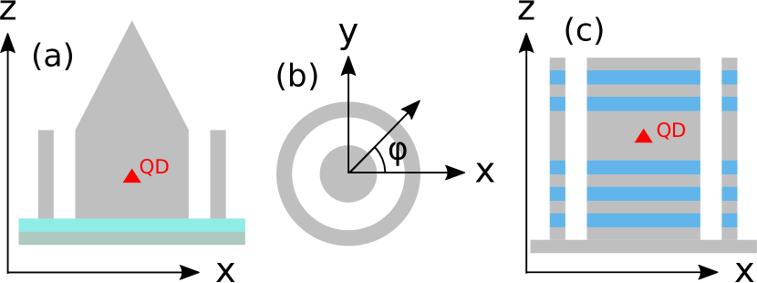
In the quest for near unity factor and collection efficiency, we explore the introduction of few-period (1-3) circular Bragg reflectors around nanowires or micropillars, in an attempt to decrease the spontaneous emission (SE) rate into background modes, . The circular Bragg reflector consists of alternating layers of air and high-index materials thus forming cylindrical rings separated by air gaps. In this paper, we will provide a detailed physical description of how cylindrical rings around an infinite nanowire can influence the emission into radiation modes referring to established literature42, 43, 44, 45, 46, 47, 48, 49, 50, 51. We will then demonstrate how the few-period circular Bragg reflector around an infinite nanowire can increase the factor of the fundamental mode () up to 0.999 due to further suppression of the emission into radiation modes caused by a photonic band gap effect. Finally, we will apply this strategy in the practically relevant case of the finite-sized SPS based on tapered nanowires sketched in Figs. (1a-1b). Additionally, we also show the beneficial effects of adding optimized high-index rings around micropillars as shown in Fig. (1c).
This paper is organized as follows: in Sec. (2), we present our theoretical framework based on the Fourier modal method and a novel analytical method. In Sec. (3), we describe the physics of the circular Bragg reflector. Subsequently, we use the analytical method to present and analyze the emission rates in the infinite nanowire (Sec. (4)) and in the infinite nanowire with rings (Sec. (5)). In Sec. (5), we also present the optimization of the factor. In Sec. (6) and Sec. (7), we present the photonic nanowire SPS with rings and the micropillar SPS with rings respectively.
2 Theory
To calculate the figures of merit we compute the total and collected power from the source by solving Maxwell’s equations in the frequency domain, modeling the QD as a classical point dipole Within the dipole approximation, the emission rate of the QD can namely be related to the classical emitted power of a dipole using the following relationship 52, where is the emitted power of the dipole and is the power emitted in a bulk medium. The factor is then defined as , where is the power emitted into our mode of interest (for instance the cavity mode or the fundamental mode) and is the total emitted power. The collection efficiency is then defined as , where is the power collected in the far-field of a lens with numerical aperture taking into account the overlap with a Gaussian shaped field profile17.
All structures considered in this paper feature cylindrical symmetry. The current distribution of the point dipole is given by: , where is the frequency, is the position of the QD and is the dipole moment. We assume that dipole is placed on-axis and the dipole orientation is in-plane. We expand the generated field upon the eigenmodes of the structure which consist of a finite set of guided modes and a continuum of radiation53. For the finite sized structures, the structure is split into layers with uniform refractive index along the z-direction and in each layer the field is expanded upon the eigenmodes. The expression for the electrical field is then given by:
| (2) |
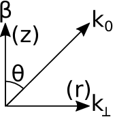
where refers to forward or backwards propagation, and are the propagation constants (not to be confused with the factor), is the mode profile, is the expansion coefficient, is the total number of guided modes, is the in-plane -value and refers to the two orthogonal solutions for the radiation modes. The guided modes are confined to regions with high refractive index, usually the core of the structure, and decay in regions with low refractive index such as air regions. Their propagation constant, , satisfy the following relation , where is the free-space -vector ( being the free-space wavelength) and we assume that the surrounding background material is air. The propagation constant of the radiation modes is related to the in-plane -value: . The radiation modes can be viewed as perturbed versions of the modes in a homogeneous air medium and are generally not confined to any specific regions. The continuum of radiation modes can be split into two parts namely the propagating radiation modes, , and the evanescent radiation modes, . For the propagating radiation modes, the propagation constant also defines the angle of propagation with respect to the z-axis: (with ), which is sketched in Fig. (2).
All the eigenmodes in Eq. (2) have angular momentum of as the dipole is placed on-axis and has in-plane orientation and thus only couples to modes with (all other modes have in-plane electrical field components of zero at ). The expansion coefficients can be derived from Lorentz reciprocity theorem53, 54 and the expressions are given in supplementary (10.6). The emitted power can then be evaluated52:
| (3) |
The resulting expressions for the power are also given in supplementary (10.6). In the infinite structures, the evanescent modes do not contribute to the power and thus one can replace the integral over all in Eq. (2) with . The total emitted power in an infinite structure can then be written as:
| (4) |
where the first term corresponds to the power into the guided modes and the second term to the power into radiation modes. We choose an orthogonalization, , such that and often we will simply use , where is the power spectrum for the radiation modes.
We have developed and used a novel method for the infinitely extending structures to analytically construct the radiation modes of a multi-layered cylindrical structure inspired by previous work55, 56, 57, 58, 53, 59, 60, 61, 62, 63, 64, 65, 66. This method allows for direct insight and efficient calculations. The method is described in supplementary (10.1&10.4) and along with the guided modes of a multi-layered cylindrical structure (supplementary 10.5). For the finite-sized structures we make use of a numerical method which also allows access to all the modes and this method is also described in supplementary (10.1).
3 Suppression of the spontaneous emission into radiation modes using a circular Bragg reflector
Multi-layered cylindrical structures have been considered in view of applications such as lasers67, 68, 69, 70, 71, 72, fibers55, 73, 74, 75, 76 and sensing77, in addition to SPSs, and their physics have been described for instance in Refs.42, 43, 44, 45, 46, 47, 48, 49, 50, 51. Just as plane waves are reflected at an interface between two materials, so are cylindrical waves; however, the main key property of cylindrically propagating waves, which are given by the Bessel functions of the first and second kind, and , is that they are non-periodic which also leads to reflections being radius dependent. This means that the typical argument for thicknesses used in planar structures when creating a photonic band gap for plane waves is no longer valid. Instead, the dimensions of each individual ring and each air gap should all be free parameters and the optimized parameters are also influenced by the total numbers of rings. However, for sufficiently large radii and/or in-plane -components the cylindrical waves approach the periodic behavior of plane waves. Ultimately, different expressions can be found, which are to either be minimized/maximized in order for instance to achieve maximum or minimum reflection or create a horizontal cavity for a specific value of . Maximizing the reflection will then lead to a photonic band gap. However, our goal is to increase the factor by suppressing the emission into radiation modes, , which consist of a continuum of cylindrically propagating waves with . We thus need to take into account all the possible values of , but translating this into a wavelength interval would result in an infinitely broad range. Fortunately, the depends on the refractive index of the material, , and inside a material is given by: , such that and here the Bessel functions take the arguments and . Thus, a high refractive index contrast effectively reduces the required width of the photonic band gap, while simultaneously increasing the reflection and the width of the photonic band gap. However, the reflected wave must not provide constructive interference at the position of the QD hereby creating a cavity, but this will be taken into account in the optimization.
To support these general considerations, we will make use of an example and consider an infinitely long wire consisting of GaAs with a diameter, , and then we add 1 and 2 rings. We use a wavelength of throughout the paper, and the refractive index of GaAs is set to be: . The in-plane cross-sectional view of the wire with 0, 1 and 2 rings is shown in Figs. (3a-3c) with the dimensions being indicated. We then select the radiation mode with and optimize the ring(s) dimensions to minimize .
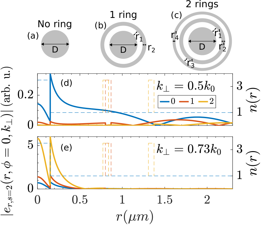
In Fig. (3d), the absolute value of the radial electrical field component for the radiation mode with is shown as a function of the radius, , for 0, 1 and 2 ring(s). Here the electrical field is strongly suppressed at for 1 ring and even more for 2 rings. The refractive index profile is also shown along with the field and the optimized ring parameters for 1 ring are given by: and . For 2 rings: , , and . This also shows that adding an extra ring can change the optimal dimensions of the first ring. However, minimizing does not ensure that is reduced for all values of and in Fig. (3e), the field is shown for the radiation mode with and here the field is actually enhanced at and thus is increased. This shows the importance of considering the entire continuum and not just one value of .
We can not solely focus on when optimizing the factor, as it also depends on both and , i.e., , where is also included in the total SE for the guided modes . The rings can namely also influence the guided modes, however, the physics of the guided modes is different from the radiation modes as they are not propagating waves in the radial direction. In the low index air regions, they are instead described by the modified Bessel functions of and , where is the in-plane component of the guided mode (in the outer air region only ). If the ring is close enough to the central wire and reaches the evanescent tails of the guided modes, the emission rates will then be influenced.
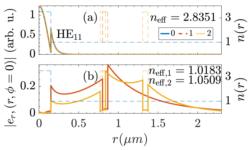
In Fig. (4a), the absolute value of the radial electrical field component for the fundamental mode is shown as a function of the radius, , for 0, 1 and 2 ring(s) with and the exact same parameters obtained from the minimization of . Here the field of the fundamental mode is not influenced at all as the rings are too far away. However, in Fig. (4b), the field is shown for two new higher order guided modes which appear due to the rings. These are weakly confined ring modes and a small part of the field extends to the wire axis; as a result, rings can influence the SE rate into guided modes. Therefore, the optimization should not focus only on reducing , and in the following we will use as the objective function to be maximized.
4 Infinitely long nanowire
The starting point of the optimization is the bare nanowire for which we will then add rings. In this section, we will therefore present the normalized emission rates of a QD with an emission wavelength of placed on-axis of an infinitely long GaAs nanowire without any rings. A sketch of the nanowire with an embedded QD is shown in Fig. (5a) and the cross-sectional view in Fig. (5b).
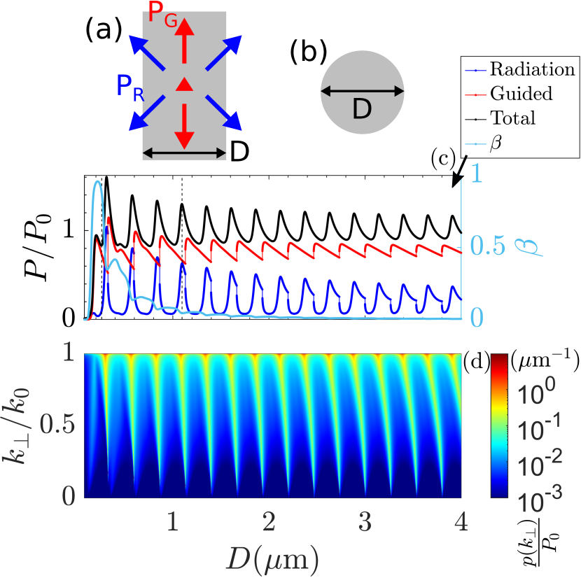
In Fig. (5c) the emission rates into the guided modes, the radiation modes and their sum is shown as a function of the wire diameter, . For the smallest diameters all emission is suppressed as the fundamental mode is weakly confined and the emission into the radiation modes is suppressed due to the dielectric screening effect25, 27. Then the power into the fundamental mode rapidly increases as the confinement of the mode increases and thus also the electrical field at the center of the wire, whereas the emission into the radiation modes is still suppressed due to the dielectric screening effect. This is also the region, where the factor (right y-axis in Fig. (5c)) is the largest and reaches a value of at . As the diameter increases, the emission into the fundamental mode decreases due to the decreased confinement and field strength and so does the factor. Furthermore, more guided modes appear and they appear in pairs where the modes provide a discontinuous increase in the SE rate, quickly peak and then decrease, whereas the SE rate contribution from the modes increase more slowly and then decrease 78. The emission into radiation modes follows a semi-periodic pattern with peaks and valleys, where the peaks increase in width and decrease in intensity as the diameter increases. These peaks also correspond to the peaks in the total emission and at these peaks there will also be dips in the factor. Furthermore, there are discontinuous decreases exactly when the new guided modes appear such that the total emission rate is continuous, which showcases the transition between the radiation modes and the guided modes.
To understand the behavior of the emission into radiation modes we need to consider the spectrum which is shown in Fig. (5d) as a function of the wire diameter. Here we observe peak lines for as a function of the diameter and these lines slowly start to bend as the diameter increases. The bending of these peak lines causes the peaks in to increase in width and decrease in intensity. The reason for why the lines bend is found by considering the behavior of each radiation mode. Each radiation mode namely experiences a reflection at the interface between the wire and the air which leads to interference between the outgoing and reflected wave at the position of the dipole, i.e., there can both be constructive and destructive interference leading to either increased or decreased emission. Therefore the emission into each radiation mode has peaks and valleys as a function of the diameter. For small diameters the period between the peaks is non-periodic due to the cylindrical nature of the modes and then approach a periodic behaviour for larger diameters. Nonetheless, the period between the peaks is determined by , and for the smallest diameters, these peaks almost overlap for all values of , but then they shift apart for increased diameters due to the different periods, which explains the bending in Fig. (5d). As such, the entire spectrum of , which we wish to minimize in order to increase the factor, will never become truly periodic.
5 Rings
We are now equipped to understand the influence of adding rings around the nanowire. A sketch of the infinite nanowire with a ring can be seen in Figs. (6a-6b). First, we consider two examples with one ring, where the diameter is fixed and the air gap, , and the ring thickness, , are varied.
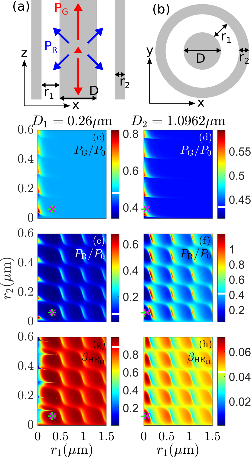
In Figs. (6c-6h) the normalized emission into the guided modes , into radiation modes , and the factor are shown as a function of the air gap, , and ring thickness, , for two selected diameters of and , both indicated by the vertical dotted lines in Fig. (5c). These diameters correspond to drastically different situations: for , the emission into radiation modes is very weak and the emission into the fundamental mode is large, while for , the emission into radiation modes is strong and the emission into the fundamental mode is weak. For the guided modes in Figs. (6c-6d), it can immediately be observed that the ring needs to be close to the central wire to influence the emission rate. This is exactly due to the evanescent field outside the center wire for the guided modes. It is the higher order modes with the smallest propagation constants which are responsible for the tails of slightly larger values of seen in Figs. (6c) and (6d). These modes namely decay the slowest outside the center wire. Additionally, weakly confined ring modes close to the wire can also influence the emission rate as discussed earlier. For the radiation modes, shown in Figs. (6e) and (6f), the rates are influenced in the entire parameter space and a semi-periodic interference pattern can be seen as a function of and , where the periods are much shorter for due to the large refractive index of GaAs. The strongest effects are observed within the first period of varying the air gap and ring thickness, i.e., here the maximum in is found indicated by the magenta crosses and the minimum in indicated by the green pluses. For , the magenta cross and green plus overlap exactly, which demonstrates that the improvement results from inhibition of SE into radiation modes. For there is a slight difference in the position of the magenta cross and green plus due to the SE contribution of the guided modes. For there is an increase in from to and for from to . For the smaller diameter the absolute increase in is larger as the dominating contribution to the background emission is which the ring can significantly reduce. Thus, already for one ring the effect of the photonic band gap can be observed. For the larger diameter, the emission into higher order guided modes contribute significantly to the background emission which the ring does not control and therefore the absolute increase in is not as large. We will nevertheless highlight in section (7), its beneficial effect for the performance of QD-micropillar SPS.
5.1 factor optimization
We will now perform an optimization of the factor (of the fundamental mode) as a function of the center diameter with respect to the ring dimensions. For one ring, the optimization is straight forward as the parameters of and can simply be scanned for each diameter as the computation is very fast due to the analytical method.
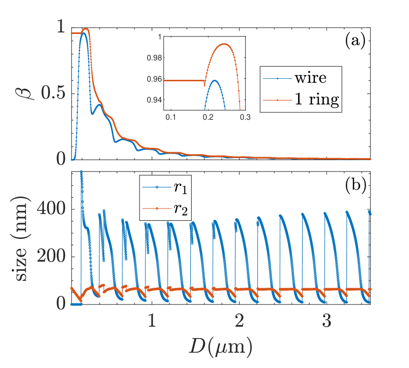
In Fig. (7a) the factor for the wire without rings and the wire with one optimized ring is shown as a function of the wire diameter. It is possible to increase the factor for all diameters and a significant increase in the maximum factor from at to at with and . As such the losses to other modes have been reduced from to such that the fraction of power lost is reduced by a factor 5.8. In Fig. (7b), the optimized parameters for the air gap and ring thickness are shown as a function of the wire diameter. For the smallest diameters the factor is constant for the wire with 1 ring since the optimization basically increased the diameter as the air gap is 0 as seen in Fig. (7b). Generally, the optimized parameters follow a semi-periodic pattern, where the air gap features the largest changes compared to the ring thickness due to the difference in the refractive index between the GaAs and air. The optimized parameters deviate most from the periodic pattern for the smallest diameters where the non-periodic nature of the radiation modes due to the cylindrical symmetry is more pronounced.
We will now also perform the optimization of the factor for the two configurations of two and three rings around the wire, where we focus on the small diameter regime. For each configuration, we perform (i) one calculation where all air gaps and ring thicknesses are treated as free parameters, and (ii) another one where all air gaps and ring thicknesses are respectively identical (which we will call "fixed" in the following). In the former case we thus have 2N free parameters (with N being the numbers of rings) for a fixed diameter, while the second case only has 2 parameters. Details on the numerical optimization are given in supplementary (10.7&10.8). As discussed earlier it is important that all associated ring parameters are free when optimizing the factor, however, we also wish to compare with fixed air gaps and ring thicknesses as this is typically used for other SPS design with cylindrical rings like the bullseye SPS.

In Fig. (8), the factor is shown as a function of the wire diameter for 1 ring, 2 rings, 2 rings with fixed parameters, 3 rings, and 3 rings with fixed parameters. As seen, it is possible to increase the factor above 0.99 in a broad diameter range and adding more rings does indeed increase the factor further. Allowing all the parameters to be free leads to a small increase in the maximum factor, and also slightly increases the width of the diameter range enabling very-high values. Still, even though the radiation modes are cylindrical waves and form a continuum, the penalty of fixing the parameters for the maximum factor is fairly small.
| no rings | 1 ring | 2 rings | 2 rings - fixed | 3 rings | 3 rings - fixed | |
| 0 | ||||||
In Table (1), the maximum factor, , , , and the corresponding diameters and ring dimensions for the optimized rings are shown. decreases for an increased numbers of rings due to an increased wire diameter, however, it is compensated for by the decreased emission into radiation modes to increase the factor. Additionally, is now so small such that , due to the higher order guided modes, is comparable in magnitude. This shows that in the absolute limit of , the emission into higher order guided modes, introduced by the rings, is equally important as the radiation modes.
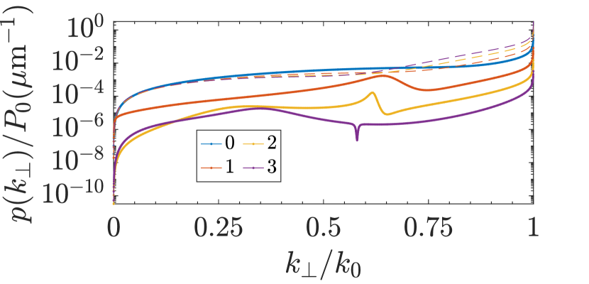
In Fig. (9), the spectra for all the different numbers of rings at the optimized parameters from Table (1) are shown as a function of . The dotted lines correspond to the optimized diameters for the different numbers of rings, but without the rings themselves to directly compare the spectra. As shown, the rings in fact very efficiently suppress the emission into radiation modes for all values of .
6 Finite-size photonic nanowire
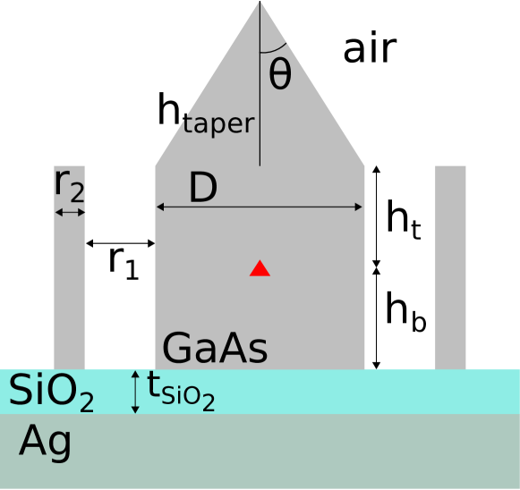
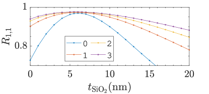
We now apply the results of the previous section, which are valid in the infinite wire approximation, to the finite sized photonic nanowire SPS79, 80, 26, 25, 27, 28, 16. We will thus compare the photonic nanowire SPS without rings to adding one, two and three rings (only the free parameters) using the optimized parameters shown in Table 1. A sketch of the photonic nanowire SPS with rings and its geometrical parameters can be seen in Fig. (10). The central part is made of a finite-length nanowire segment, capped by a conical needle taper with half-opening angle and a total taper height of . The purpose of the needle taper is to adiabatically transform the fundamental mode to increase the collection efficiency79, 28. At the interface between the wire and the taper, the surrounding rings, if any are added, have the same length as the nanowire segment and are terminated by a flat top surface. At the bottom there is a - mirror81, where the has a thickness of . For the refractive indices we use: and . The QD is placed at a distance () from the bottom (top) interface.
We will compare the full model, , with the single-mode model efficiency80:
| (5) |
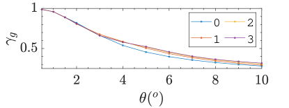
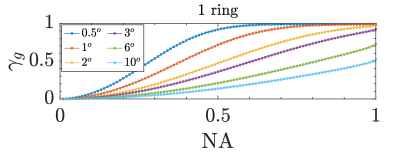
where is the transmission coefficient of the fundamental mode. is the factor of the infinite structure and is the modal reflection of the fundamental mode at the bottom interface. In the derivation of the SMM of Eq. (5), it is assumed that the top reflection is close to 0. In supplementary (10.9), we show that the maximum reflection of the fundamental mode at the bottom interface is obtained at for all the different numbers of rings (including no ring). We also show how changes as a function of the tapering angle, , and the . Additionally, we show that the top reflection approaches 0 for small tapering angles, but does increase for larger tapering angles.
The vertical position of the dipole also needs to be determined and it should be placed at an antinode. For small angles of , the reflection of the fundamental mode at the top interface is approximately 0 and in this case there is no condition for the top height, . However, when the angle increases there will be a reflection and within the picture of a single-mode model both the top and bottom height, and , need to satisfy:
| (6) |
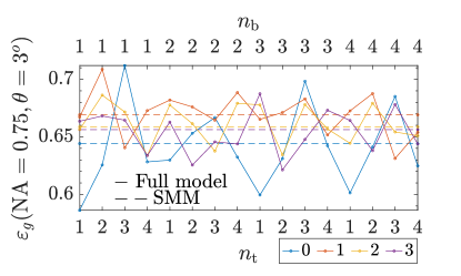
where is the propagation constant of the fundamental mode. () thus determines the number of antinodes from the bottom (top) interface to the position of the dipole. Within the single-mode model, the choice of should have minimum influence on the performance of the structure, but as we will show it can indeed influence both the efficiency and the factor (shown in supplementary (10.9)) thereby deviating from the single-mode model. As such we have tested the combined set of resulting in a total of 16 combinations.
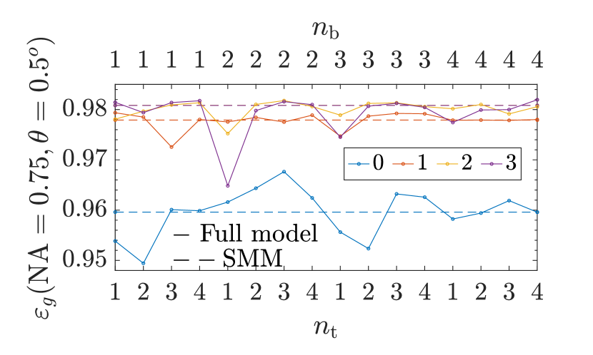
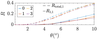
In Fig. (11), the collection efficiency, , is shown as a function of the 16 different combinations of and for the different numbers of rings at a tapering angle of . The dotted line is calculated using the SMM while the solid line is the full model. Even though the top reflection is very small there are still deviations between the full model and the SMM for all the different numbers of rings, resulting in a breakdown of the SMM. These deviation can both be positive and negative, but in general these deviations are negative except for no rings where there can be an increase of 0.0075 for and . These deviations can be explained by the evanescent modes as there is still coupling between the fundamental mode and the evanescent modes at the interfaces, which is not quantified by the power reflections nor by the emission rates in the infinite structure. This effect decreases the further away the dipole is from interfaces as the evanescent modes decay which corresponds to larger values of and . However, it could indicate that in a complete optimization of the collection efficiency, the optimal heights of and could slightly deviate from the SMM heights. A similar effect occurs for the nanopost SPS82 and this effect could be quantified using the same models as in Ref.82. Ultimately, the maximum collection efficiencies obtained for the selected heights and are: , , and with a total increase of 0.0143 in the maximum collection efficiency from no ring to 3 rings. The maximum collection efficiencies for the rings do not reach the values of the factors in the infinite structures. This is because the limiting factors are now the bottom reflection and the transmission through the top taper. Nonetheless, for a multi-photon experiment with 50 photons the success probability increases by a factor of . This demonstrates that the efficiency increase, obtained by suppressing the background emission using the dielectric rings, can have a significant impact on the scale-up of photonics experiment.
For larger tapering angles, the collection efficiency is even more sensitive to the heights as is shown in supplementary (10.9).
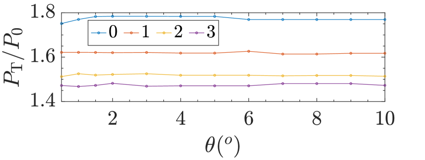
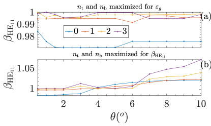
The Purcell factor of the total emission, , is shown in Fig. (12) as a function of the tapering angle, , for the different numbers of rings where and are chosen such that is maximised. does not change significantly as a function of the tapering angle. As expected, depends on the numbers of rings and this is directly related to the center diameter as for the infinite structures.

In Fig. (13) the collection efficiency, , is shown as a function of the tapering angle, , for the different numbers of rings where and are chosen such that is maximised. The collection efficiency follows the curve for the transmission coefficient, , shown in Fig. (20) found in supplementary (10.9), with some deviations. Generally, the collection efficiency decreases as a function of the tapering angle due to the decreased transmission coefficient. As already shown for , the collection efficiency can be increased for the smallest tapering angles, , using the rings. Between and , no ring performs slightly better than any of the other numbers of rings, while above , no ring performs the worst.
7 Micropillar
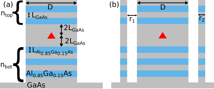
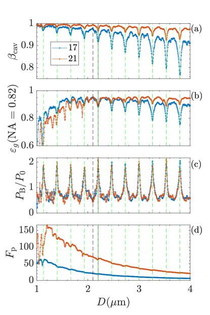
We now add rings around a micropillar SPS and show that this can improve the performance. Such a device has been investigated numerically83, however, without a clear improvement in the performance. It has also been investigated for a half-micropillar SPS in the telecom O-band84, where improvements were possible for the collection efficiency, but without reaching the performance of state-of-the-art numerically optimized SPS micropillars17. Cylindrical dielectric DBRs around the micropillar SPS have also been realized experimentally85, where the off-resonance SE rate was decreased compared to the bulk SE rate indicating that had been suppressed. However, the study did not include numerical simulations to analyze the improvement. Here we will consider state-of-the-art numerically optimized micropillar SPSs17 and demonstrate how the rings can further improve the performance. The optimized micropillar SPS features both large collection efficiency and indistinguishability simultaneously17. A sketch of the micropillar with and without rings and the geometrical parameters can be seen in Fig. (14). The materials are GaAs and with . The DBR layer thicknesses are diameter dependent given by , where is the effective index of the fundamental mode in the GaAs or the obtained from the propagation constant (). The cavity thickness is and the dipole is placed in the center. The bottom (top) DBR contains () layer pairs. The cavity mode of the micropillar SPS is almost identical to the fundamental mode17, and we will be using for the factor (Eq. (1)).
As mentioned in the introduction, the micropillar SPS utilizes the Purcell effect to increase and thus also features large values of . Generally, peaks around and then decreases for increased diameters due to an increased mode volume17. This behavior is reflected in which also decreases. However, more importantly to this work is the background emission of the micropillar. For the micropillar SPS, both radiation modes and higher order guided modes contribute to . of the micropillar is very much diameter dependent, however, it does not follow the peaks of the total emission rate in the infinite wire as in Fig. (5c). Instead, features pronounced peaks exactly at the onset of the guided modes and these peaks lead to dips in and 78, but with limited effect on 17. These peaks thus consist on the lower diameter side of radiation modes and on the larger diameter side the newly appeared guided mode. In supplementary (10.10), we have reproduced , , , and of the best performing micropillars17 with and or . We will now choose two different diameters and add a ring. One diameter, , corresponds to a peak in and the other diameter, , corresponds to a local minimum in and thus a maximum in and . The micropillar with is therefore an optimized micropillar SPS with respect to the diameter. When the ring is added, the propagation constant of the fundamental mode, , does change very slightly, so that it should not have any influence when the first air gap is above . Nonetheless, this has been accounted for in the following simulation. In the following we will be using .
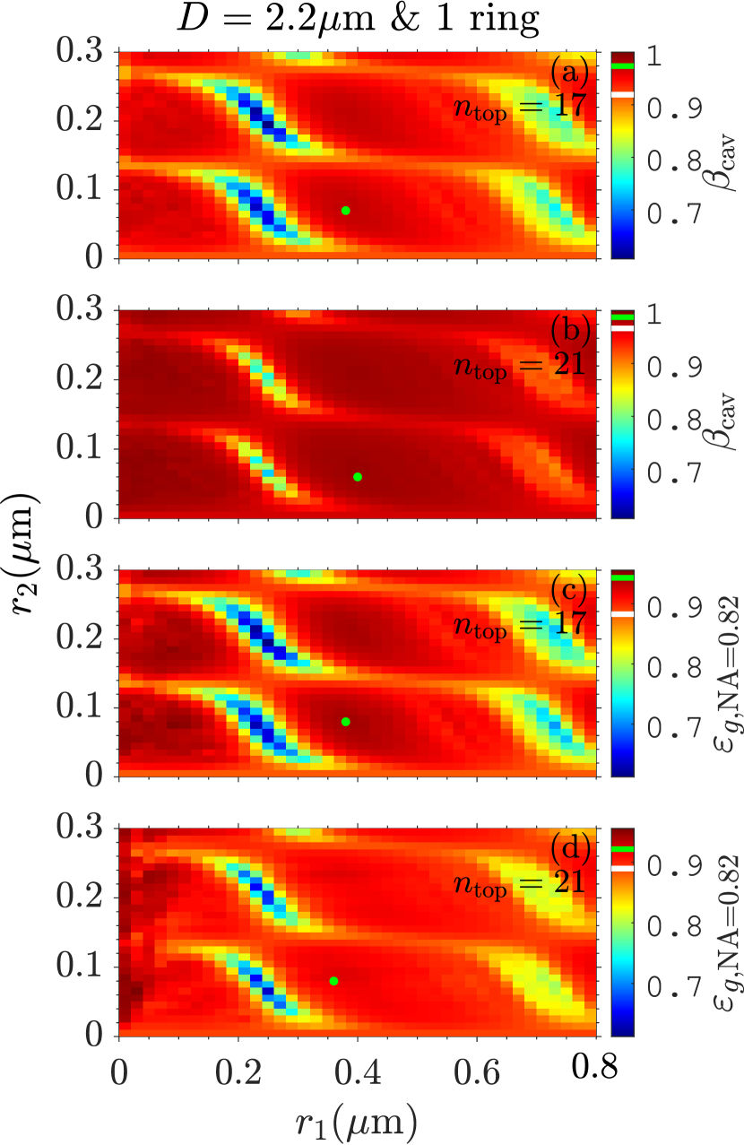
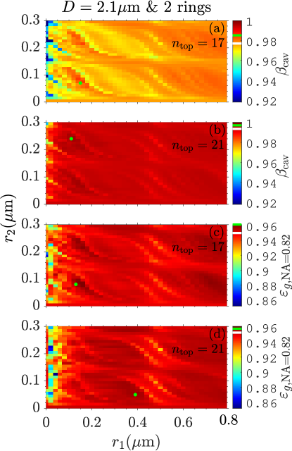
In Fig. (15), the (a) with , (b) with , (c) with , and (d) with are shown as a function of the air gap, , and the ring thickness, , for 1 ring at . The first trend observed in Fig. (15) is that regions with increased also show an increased , which is similar to the trend seen in the micropillar without any rings. Following the vertical axis simply corresponds to increasing the diameter and this will lead to an increase in and , but we are interested in whether an actual ring with an air gap can increase the performance. This is indeed possible and for some regions with there is an increase both in and . The green dots indicate the maximum values with the restrictions of and . For and the following increases are obtained: from to (1 ring) with and . For : from to with and . The ring has thus efficiently suppressed the background emission into radiation modes and close-to-cutoff guided modes, which are at the origin of the performance decrease for a micropillar. Therefore the ring improves the performance of this micropillar to values that are very close to the ones of a micropillar with an optimal diameter.
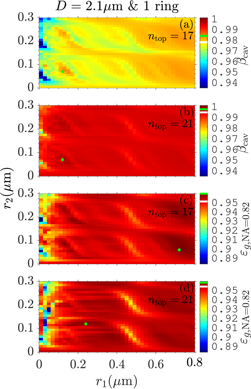
In Fig. (16), we now present the same scan of the ring parameters as in Fig. (15) but now for . Again, regions with an increased generally overlap with an increased , however, with some deviations for . Ultimately, the collection efficiency can be increased from to at and and for from to at and . As such the ring can still slightly improve the performance of the micropillar with an optimal diameter. However, a major part of the background emission is into higher order guided modes and the ring offers no suppression mechanism of these modes and therefore is not reduced to the same level as for the small diameter range of the infinite wire.
In supplementary (10.10), we also show and for 2 rings with fixed parameters surrounding the micropillar with . Here the collection efficiency reaches a maximum of at and . Thus, with the test of 1 to 2 rings around the micropillar showing a potential increase in the collection efficiency of from with no rings to with 2 rings, corresponding to a reduction in the losses from 4.7% to 3.9%, we have shown that the rings can indeed further push the boundary of the optimized micropillar.
8 Discussion
We have shown that a few rings around the infinite wire can increase the factor up to 0.99 in the small diameter regime of to by suppressing the emission into radiation modes. For two and three rings it was even possible to achieve a factor up to 0.999. We then applied this result to the photonic nanowire SPS, which led to an increase in the maximum collection efficiency obtained at the smallest tapering angles, . The reason for why we could directly apply the result of the infinite wire is that the physics of the photonic nanowire is generally viewed as single-moded80. There is only one guided mode, the fundamental mode, due to the small diameter and the fundamental mode does not scatter significantly into radiation modes at the optimized bottom mirror, nor any back-scattering at the top needle taper with a small tapering angle. However, we also varied the position of the dipole by placing it at different antinodes and here we observed fairly significant deviations from the SMM. This could be explained by the coupling to and from the evanescent modes and as such leaves room for further optimization of the height of the straight nanowire section and the position of the dipole. Still, the limiting factors to increase the collection efficiency towards unity for the photonic nanowire SPS are the transmission coefficient and the bottom reflection. One extra detail is that for each added ring, the diameter of the central nanowire for the maximum value of the factor slightly increased. This leads to slightly longer structures for the needle tapering, but this would instead be an advantage for trumpet tapers80, 28, 86, 16, 87.
For larger diameters, it was also possible to increase the factor of the infinite wire. However, the absolute increase was not as large as for the smaller diameters, because it is the higher-order guided modes which constitute the main contribution to the background emission, for which the rings do not offer any control. Still, we wanted to put rings around the micropillar SPS which typically features diameters in the - range. However, the background emission, , of the micropillar follows a different pattern than the background emission of the infinite wire and therefore we could not directly apply the optimized ring parameters of the infinite wire to the micropillar. Nonetheless, at a suboptimal diameter where peaks, the ring could suppress close to a level of an optimal diameter such that the collection efficiency significantly increased. At an optimal diameter, 1-2 rings could still slightly increase the collection efficiency. However, we observe in Fig. (16) slightly different behaviours between the factor and the collection efficiency. This shows that a SMM is not sufficient to capture fully the effects of the rings. The demanding complete optimization of micropillars with rings, using the full modal model presented in this paper, goes beyond the scope of the present paper and is left for future work.
9 Conclusions
We have provided a detailed physical description of how cylindrical rings around an infinite wire influence the emission rates into the guided modes and the radiation modes. This was done by making use of a fully analytical method, allowing for in-depth analysis and fast computations. We then demonstrated that a few rings could further suppress the emission into radiation modes, such that we could achieve factors up to 0.999. This result was then applied to the photonic nanowire SPS, which led to an increase in the maximum collection efficiency from without any rings to with three rings; further pushing the theoretical limit toward near-unity collection efficiency. This increase in the collection efficiency corresponds to an increase in the success probability of a multi-photon interference experiment with 50 photons by a factor of . We also simulated rings around the micropillar SPS for which it was also possible to further increase the collection efficiency from to .
Author Contributions
N.G. formulated the project. M.A.J. developed the analytical method and performed the simulations. M.A.J. wrote the manuscript with comments from all authors. N.G. and L.V. supervised the project.
Conflicts of interest
There are no conflicts to declare.
Acknowledgements
This work is funded by the European Research Council (ERC-CoG “UNITY,” Grant No. 865230), the French National Research Agency (Grant No. ANR-19-CE47-0009-02), the European Union’s Horizon 2020 Research and Innovation Programme under the Marie Skłodowska-Curie Grant (Agreement No. 861097), and by the Independent Research Fund Denmark (Grant No. DFF-9041-00046B).
References
- Arakawa and Holmes 2020 Y. Arakawa and M. J. Holmes, Appl. Phys. Rev., 2020, 7, 021309.
- Aharonovich et al. 2016 I. Aharonovich, D. Englund and M. Toth, Nat. Photonics, 2016, 10, 631–641.
- Gregersen et al. 2013 N. Gregersen, P. Kaer and J. Mørk, IEEE J. Sel. Top. Quantum Electron., 2013, 19, 9000516.
- Gregersen et al. 2017 N. Gregersen, D. P. S. McCutcheon and J. Mørk, Handbook of Optoelectronic Device Modeling and Simulation Vol. 2, CRC Press, Boca Raton, 2017, ch. 46, pp. 585–607.
- Huber et al. 2018 D. Huber, M. Reindl, J. Aberl, A. Rastelli and R. Trotta, J. Opt., 2018, 20, 073002.
- Pan et al. 2012 J.-W. Pan, Z.-B. Chen, C.-Y. Lu, H. Weinfurter, A. Zeilinger and M. Zukowski, Rev. Mod. Phys., 2012, 84, 777–838.
- O’Brien et al. 2009 J. L. O’Brien, A. Furusawa and J. Vučković, Nat. Photonics, 2009, 3, 687–695.
- Gérard and Gayral 1999 J.-M. Gérard and B. Gayral, Journal of Lightwave Technology, 1999, 17, 2089–2095.
- Michler et al. 2000 P. Michler, A. Kiraz, C. Becher, W. V. Schoenfeld, P. M. Petroff, L. Zhang, E. Hu and A. Imamoglu, Science, 2000, 290, 2282–2285.
- Santori et al. 2002 C. Santori, D. Fattal, J. Vučković, G. S. Solomon and Y. Yamamoto, Nature, 2002, 419, 594–597.
- Shields 2007 A. J. Shields, Nat. Photonics, 2007, 1, 215–223.
- Barnes et al. 2002 W. L. Barnes, G. Björk, J. M. Gérard, P. Jonsson, J. A. E. Wasey, P. T. Worthing and V. Zwiller, The European Physical Journal D - Atomic, Molecular, Optical and Plasma Physics, 2002, 18, 197–210.
- Gérard et al. 1998 J. M. Gérard, B. Sermage, B. Gayral, B. Legrand, E. Costard and V. Thierry-Mieg, Phys. Rev. Lett., 1998, 81, 1110–1113.
- Purcell 1946 E. M. Purcell, Phys. Rev., 1946, 69, 681.
- Friedler et al. 2009 I. Friedler, C. Sauvan, J. P. Hugonin, P. Lalanne, J. Claudon and J. M. Gérard, Opt. Express, 2009, 17, 2095–2110.
- Gregersen et al. 2016 N. Gregersen, D. P. S. McCutcheon, J. Mørk, J.-M. Gérard and J. Claudon, Opt. Express, 2016, 24, 20904–20924.
- Wang et al. 2020 B.-Y. Wang, E. V. Denning, U. M. Gür, C.-Y. Lu and N. Gregersen, Phys. Rev. B, 2020, 102, 125301.
- Somaschi et al. 2016 N. Somaschi, V. Giesz, L. De Santis, J. C. Loredo, M. P. Almeida, G. Hornecker, S. L. Portalupi, T. Grange, C. Antón, J. Demory, C. Gómez, I. Sagnes, N. D. Lanzillotti-Kimura, A. Lemaítre, A. Auffeves, A. G. White, L. Lanco and P. Senellart, Nat. Photonics, 2016, 10, 340–345.
- Moreau et al. 2001 E. Moreau, I. Robert, J. M. Gérard, I. Abram, L. Manin and V. Thierry-Mieg, Applied Physics Letters, 2001, 79, 2865–2867.
- Wang et al. 2019 H. Wang, Y.-M. He, T.-H. Chung, H. Hu, Y. Yu, S. Chen, X. Ding, M.-C. Chen, J. Qin, X. Yang, R.-Z. Liu, Z.-C. Duan, J.-P. Li, S. Gerhardt, K. Winkler, J. Jurkat, L.-J. Wang, N. Gregersen, Y.-H. Huo, Q. Dai, S. Yu, S. Höfling, C.-Y. Lu and J.-W. Pan, Nat. Photonics, 2019, 13, 770–775.
- Ding et al. 2016 X. Ding, Y. He, Z.-C. Duan, N. Gregersen, M.-C. Chen, S. Unsleber, S. Maier, C. Schneider, M. Kamp, S. Höfling, C.-Y. Lu and J.-W. Pan, Phys. Rev. Lett., 2016, 116, 020401.
- Tomm et al. 2021 N. Tomm, A. Javadi, N. O. Antoniadis, D. Najer, M. C. Löbl, A. R. Korsch, R. Schott, S. R. Valentin, A. D. Wieck, A. Ludwig and R. J. Warburton, Nat. Nanotechnol., 2021, 16, 399–403.
- Iles-Smith et al. 2017 J. Iles-Smith, D. P. S. McCutcheon, A. Nazir and J. Mørk, Nature Photonics, 2017, 11, 521–526.
- Gaál et al. 2022 B. Gaál, L. Vannucci, M. A. Jacobsen, J. Claudon, J.-M. Gérard and N. Gregersen, Applied Physics Letters, 2022, 121, 170501.
- Bleuse et al. 2011 J. Bleuse, J. Claudon, M. Creasey, N. S. Malik, J.-M. Gérard, I. Maksymov, J.-P. Hugonin and P. Lalanne, Phys. Rev. Lett., 2011, 106, 103601.
- Claudon et al. 2010 J. Claudon, J. Bleuse, N. S. Malik, M. Bazin, P. Jaffrennou, N. Gregersen, C. Sauvan, P. Lalanne and J.-M. Gérard, Nat. Photonics, 2010, 4, 174–177.
- Claudon et al. 2013 J. Claudon, N. Gregersen, P. Lalanne and J.-M. Gérard, ChemPhysChem, 2013, 14, 2393–2402.
- Munsch et al. 2013 M. Munsch, N. S. Malik, E. Dupuy, A. Delga, J. Bleuse, J.-M. Gérard, J. Claudon, N. Gregersen and J. Mørk, Phys. Rev. Lett., 2013, 110, 177402.
- Lecamp et al. 2007 G. Lecamp, P. Lalanne and J. P. Hugonin, Phys. Rev. Lett., 2007, 99, 023902.
- Manga Rao and Hughes 2007 V. S. C. Manga Rao and S. Hughes, Phys. Rev. B, 2007, 75, 205437.
- Arcari et al. 2014 M. Arcari, I. Söllner, A. Javadi, S. Lindskov Hansen, S. Mahmoodian, J. Liu, H. Thyrrestrup, E. H. Lee, J. D. Song, S. Stobbe and P. Lodahl, Phys. Rev. Lett., 2014, 113, 093603.
- Zhou et al. 2022 X. Zhou, P. Lodahl and L. Midolo, Quantum Science and Technology, 2022, 7, 025023.
- Da Lio et al. 2022 B. Da Lio, C. Faurby, X. Zhou, M. L. Chan, R. Uppu, H. Thyrrestrup, S. Scholz, A. D. Wieck, A. Ludwig, P. Lodahl and L. Midolo, Advanced Quantum Technologies, 2022, 5, 2200006.
- Østfeldt et al. 2022 F. T. Østfeldt, E. M. González-Ruiz, N. Hauff, Y. Wang, A. D. Wieck, A. Ludwig, R. Schott, L. Midolo, A. S. Sørensen, R. Uppu and P. Lodahl, PRX Quantum, 2022, 3, 020363.
- Davanço et al. 2011 M. Davanço, M. T. Rakher, D. Schuh, A. Badolato and K. Srinivasan, Applied Physics Letters, 2011, 99, 041102.
- Ates et al. 2012 S. Ates, L. Sapienza, M. Davanco, A. Badolato and K. Srinivasan, IEEE Journal of Selected Topics in Quantum Electronics, 2012, 18, 1711–1721.
- Yao et al. 2018 B. Yao, R. Su, Y. Wei, Z. Liu, T. Zhao and J. Liu, J. Korean Phys. Soc., 2018, 73, 1502–1505.
- Liu et al. 2019 J. Liu, R. Su, Y. Wei, B. Yao, S. F. C. da Silva, Y. Yu, J. Iles-Smith, K. Srinivasan, A. Rastelli, J. Li and X. Wang, Nat. Nanotechnol., 2019, 14, 586–593.
- Wang et al. 2019 H. Wang, H. Hu, T.-H. Chung, J. Qin, X. Yang, J.-P. Li, R.-Z. Liu, H.-S. Zhong, Y.-M. He, X. Ding, Y.-H. Deng, Q. Dai, Y.-H. Huo, S. Höfling, C.-Y. Lu and J.-W. Pan, Phys. Rev. Lett., 2019, 122, 113602.
- Rickert et al. 2019 L. Rickert, T. Kupko, S. Rodt, S. Reitzenstein and T. Heindel, Opt. Express, 2019, 27, 36824–36837.
- Moczała-Dusanowska et al. 2020 M. Moczała-Dusanowska, L. Dusanowski, O. Iff, T. Huber, S. Kuhn, T. Czyszanowski, C. Schneider and S. Höfling, ACS Photonics, 2020, 7, 3474–3480.
- Jiang and Hacker 1993 Y. Jiang and J. Hacker, Applied Physics Letters, 1993, 63, 1453–1455.
- Jiang and Hacker 1994 Y. Jiang and J. Hacker, Appl. Opt., 1994, 33, 7431–7434.
- Jiang and Hacker 1994 Y. Jiang and J. Hacker, Cylindrical-wave controlling, generating and guiding devices, 1994, US Patent 5,357,591.
- Nikolaev et al. 1999 V. V. Nikolaev, G. S. Sokolovskii and M. A. Kaliteevskii, Semiconductors, 1999, 33, 147–152.
- Kaliteevski et al. 1999 M. A. Kaliteevski, R. A. Abram, V. V. Nikolaev and G. S. Sokolovski, Journal of Modern Optics, 1999, 46, 875–890.
- Kaliteevski et al. 2000 M. A. Kaliteevski, R. A. Abram and V. V. Nikolaev, Journal of Modern Optics, 2000, 47, 677–684.
- Kaliteevskii and Nikolaev 2000 M. A. Kaliteevskii and V. V. Nikolaev, Technical Physics, 2000, 45, 865–869.
- Ochoa et al. 2000 D. Ochoa, R. Houdré, M. Ilegems, H. Benisty, T. F. Krauss and C. J. M. Smith, Phys. Rev. B, 2000, 61, 4806–4812.
- Scheuer and Yariv 2003 J. Scheuer and A. Yariv, Opt. Express, 2003, 11, 2736–2746.
- Scheuer and Yariv 2003 J. Scheuer and A. Yariv, J. Opt. Soc. Am. B, 2003, 20, 2285–2291.
- Novotny and Hecht 2012 L. Novotny and B. Hecht, Principles of Nano-Optics, Cambridge University Press, 2012.
- Nyquist et al. 1981 D. P. Nyquist, D. R. Johnson and S. V. Hsu, J. Opt. Soc. Am., 1981, 71, 49–54.
- Lavrinenko et al. 2014 A. Lavrinenko, J. Lægsgaard, N. Gregersen, F. Schmidt and T. Søndergaard, Numerical Methods in Photonics, CRC Press, 2014.
- Yeh et al. 1978 P. Yeh, A. Yariv and E. Marom, J. Opt. Soc. Am., 1978, 68, 1196–1201.
- Manenkov 1970 A. B. Manenkov, Radiophysics and Quantum Electronics, 1970, 13, 578–586.
- Snyder 1971 A. W. Snyder, IEEE Transactions on Microwave Theory and Techniques, 1971, 19, 720–727.
- Sammut 1975 R. A. Sammut, PhD thesis, The Australian National University, 1975.
- Vassallo 1981 C. Vassallo, J. Opt. Soc. Am., 1981, 71, 1282–1282.
- Shevchenko 1982 V. V. Shevchenko, Radio Science, 1982, 17, 229–231.
- Sammut 1982 R. A. Sammut, J. Opt. Soc. Am., 1982, 72, 1335–1337.
- Vassallo 1983 C. Vassallo, J. Opt. Soc. Am., 1983, 73, 680–683.
- Snyder and Love 1983 A. W. Snyder and J. D. Love, Optical waveguide theory, Springer New York, NY, 1983.
- Tigelis et al. 1987 I. Tigelis, C. N. Capsalis and N. K. Uzunoglu, International Journal of Infrared and Millimeter Waves, 1987, 8, 1053–1068.
- Morita 1988 N. Morita, Journal of Electromagnetic Waves and Applications, 1988, 2, 445–457.
- Alvarez and Xiao 2005 L. Alvarez and M. Xiao, Journal of Electromagnetic Waves and Applications, 2005, 19, 933–951.
- Scheuer et al. 2004 J. Scheuer, W. M. J. Green, G. DeRose and A. Yariv, Opt. Lett., 2004, 29, 2641–2643.
- Scheuer et al. 2005 J. Scheuer, W. M. J. Green, G. A. DeRose and A. Yariv, Applied Physics Letters, 2005, 86, 251101.
- Scheuer et al. 2005 J. Scheuer, W. Green, G. DeRose and A. Yariv, IEEE Journal of Selected Topics in Quantum Electronics, 2005, 11, 476–484.
- Scheuer 2007 J. Scheuer, J. Opt. Soc. Am. B, 2007, 24, 2178–2184.
- Jebali et al. 2007 A. Jebali, D. Erni, S. Gulde, R. F. Mahrt and W. Bächtold, J. Opt. Soc. Am. B, 2007, 24, 906–915.
- Weiss and Scheuer 2010 O. Weiss and J. Scheuer, Applied Physics Letters, 2010, 97, 251108.
- Doran and Blow 1983 N. Doran and K. Blow, Journal of Lightwave Technology, 1983, 1, 588–590.
- Johnson et al. 2001 S. G. Johnson, M. Ibanescu, M. Skorobogatiy, O. Weisberg, T. D. Engeness, M. Soljačić, S. A. Jacobs, J. D. Joannopoulos and Y. Fink, Opt. Express, 2001, 9, 748–779.
- Doran and Blow 1983 N. Doran and K. Blow, Journal of Lightwave Technology, 1983, 1, 588–590.
- Vienne et al. 2004 G. Vienne, Y. Xu, C. Jakobsen, H. Deyerl, T. Hansen, B. Larsen, J. Jensen, T. Sorensen, M. Terrel, Y. Huang, R. Lee, N. Mortensen, J. Broeng, H. Simonsen, A. Bjarklev and A. Yariv, Optical Fiber Communication Conference, 2004. OFC 2004, 2004, pp. 3 pp. vol.2–.
- Scheuer et al. 2004 J. Scheuer, W. M. J. Green, G. DeRose and A. Yariv, 2004, 5333, 183 – 194.
- Wang et al. 2021 B.-Y. Wang, T. Häyrynen, L. Vannucci, M. A. Jacobsen, C.-Y. Lu and N. Gregersen, Applied Physics Letters, 2021, 118, 114003.
- Gregersen et al. 2008 N. Gregersen, T. R. Nielsen, J. Claudon, J.-M. Gérard and J. Mørk, Opt. Lett., 2008, 33, 1693–1695.
- Gregersen et al. 2010 N. Gregersen, T. R. Nielsen, J. Mørk, J. Claudon and J.-M. Gérard, Opt. Express, 2010, 18, 21204–21218.
- Friedler et al. 2008 I. Friedler, P. Lalanne, J. P. Hugonin, J. Claudon, J. M. Gérard, A. Beveratos and I. Robert-Philip, Opt. Lett., 2008, 33, 2635–2637.
- Jacobsen et al. 2023 M. A. Jacobsen, Y. Wang, L. Vannucci, J. Claudon, J.-M. Gérard and N. Gregersen, Nanoscale, 2023, 15, 6156–6169.
- Ho et al. 2007 Y.-L. D. Ho, T. Cao, P. S. Ivanov, M. J. Cryan, I. J. Craddock, C. J. Railton and J. G. Rarity, IEEE Journal of Quantum Electronics, 2007, 43, 462–472.
- Blokhin et al. 2021 S. A. Blokhin, M. A. Bobrov, N. A. Maleev, J. N. Donges, L. Bremer, A. A. Blokhin, A. P. Vasil’ev, A. G. Kuzmenkov, E. S. Kolodeznyi, V. A. Shchukin, N. N. Ledentsov, S. Reitzenstein and V. M. Ustinov, Opt. Express, 2021, 29, 6582–6598.
- Jakubczyk et al. 2014 T. Jakubczyk, H. Franke, T. Smoleński, M. Ściesiek, W. Pacuski, A. Golnik, R. Schmidt-Grund, M. Grundmann, C. Kruse, D. Hommel and P. Kossacki, ACS Nano, 2014, 8, 9970–9978.
- Stepanov et al. 2015 P. Stepanov, A. Delga, N. Gregersen, E. Peinke, M. Munsch, J. Teissier, J. Mørk, M. Richard, J. Bleuse, J.-M. Gérard and J. Claudon, Applied Physics Letters, 2015, 107, 141106.
- Cadeddu et al. 2016 D. Cadeddu, J. Teissier, F. R. Braakman, N. Gregersen, P. Stepanov, J.-M. Gérard, J. Claudon, R. J. Warburton, M. Poggio and M. Munsch, Applied Physics Letters, 2016, 108, 011112.
- Gür et al. 2021 U. M. Gür, S. Arslanagić, M. Mattes and N. Gregersen, Phys. Rev. E, 2021, 103, 033301.
- Häyrynen et al. 2016 T. Häyrynen, J. R. de Lasson and N. Gregersen, Journal of the Optical Society of America A, 2016, 33, 1298.
- Balanis 1989 C. A. Balanis, Advanced Engineering Electromagnetics, Wiley, New York, 1st edn, 1989.
- Yariv and Yeh 2007 A. Yariv and P. Yeh, Photonics: Optical Electronics in Modern Communications , Oxford University Press, 6th edn, 2007.
- Yeh and Lindgren 1977 C. Yeh and G. Lindgren, Appl. Opt., 1977, 16, 483–493.
- Morishita et al. 1982 K. Morishita, Y. Obata and N. Kumagai, IEEE Transactions on Microwave Theory and Techniques, 1982, 30, 1821–1826.
- Kaliteevskiĭ et al. 2000 M. A. Kaliteevskiĭ, V. V. Nikolaev and R. A. Abram, Optics and Spectroscopy, 2000, 88, 792–795.
- Ko and Sambles 1988 D. Y. K. Ko and J. R. Sambles, J. Opt. Soc. Am. A, 1988, 5, 1863–1866.
- García and Gasulla 2020 S. García and I. Gasulla, IEEE Journal of Selected Topics in Quantum Electronics, 2020, 26, 1–11.
- Xie and Zhang 2022 X. Xie and Y. Zhang, Journal of Lightwave Technology, 2022, 40, 785–796.
- Inc. 2021 T. M. Inc., MATLAB version: 9.11.0 (R2021b), 2021, https://www.mathworks.com.
- Langbein et al. 2009 U. Langbein, U. Trutschel, A. Unger and M. Duguay, Optical and Quantum Electronics, 2009, 41, 223–233.
- Chew 1984 W. C. Chew, GEOPHYSICS, 1984, 49, 81–91.
- Lovell and Chew 1987 J. R. Lovell and W. C. Chew, IEEE Transactions on Geoscience and Remote Sensing, 1987, GE-25, 850–858.
- Chew 1995 W. C. Chew, Waves and Fields in Inhomogenous Media, Wiley-IEEE Press, 1995.
- Bhattacharya et al. 2020 D. Bhattacharya, B. Ghosh, M. Sinha and A. A. Kishk, IET Microwaves, Antennas & Propagation, 2020, 14, 1027–1037.
- Hong 2022 D. Hong, IEEE Transactions on Geoscience and Remote Sensing, 2022, 60, 1–16.
- Arfken and Weber 2005 G. B. Arfken and H. J. Weber, Mathematical Methods for Physicists (sixth Edition), Elsevier Academic Press, Boston, sixth Edition edn, 2005, pp. 675–739.
- Uzunoglu et al. 1987 N. K. Uzunoglu, C. N. Capsalis and I. Tigelis, J. Opt. Soc. Am. A, 1987, 4, 2150–2157.
- Inc. 2023 T. M. Inc., fmincon, 2023, https://se.mathworks.com/help/optim/ug/fmincon.html.
- Inc. 2023 T. M. Inc., fminsearch, 2023, https://se.mathworks.com/help/matlab/ref/fminsearch.html.
- D’Errico 2023 J. D’Errico, fminsearchbnd,fminsearchcon, 2023, https://www.mathworks.com/matlabcentral/fileexchange/8277-fminsearchbnd-fminsearchcon.
- Inc. 2023 T. M. Inc., patternsearch, 2023, https://se.mathworks.com/help/gads/patternsearch.html.
10 Supplementary
10.1 Numerical methods
For the structures which extend infinitely the eigenmodes will be found analytically, whereas for the finite sized structures the eigenmodes will be found using the FMM with open boundary conditions88 and a non-equidistant discretization scheme89, 88 which can easily be combined with a standard scattering matrix formalism54 to calculate the electromagnetic field and the normalized emission rates. A near- to far-field transformation is then utilized90 along with a Gaussian field overlap (see appendix of Ref.17) to calculate the collection efficiency.
We will now provide a bit more information on how the eigenmodes can be found analytically. There are several studies and articles of the radiation modes of a dielectric wire or more generally a waveguide with open boundary conditions56, 57, 58, 53, 59, 60, 61, 62, 63, 64, 65, 66. Here we will also consider structures with more layers in the radial direction compared to the nanowire, but still the orthogonalization condition/procedure is exactly the same and the transfer matrix formalism for cylindrical structures55 can easily be applied to obtain the continuum of radiation modes for arbitrary radial index profiles with cylindrical symmetry. To the best of our knowledge, the radiation modes for such a structure have not been explicitly constructed before. The mathematical formulation will be outlined in the following sections.
Descriptions of the guided modes of the wire are text-book material91, while for cylindrical structures with additional layers there are several different analytical methods to describe the guided modes. Variations of the transfer matrix formalism92, 93, 94 can be used to obtain the guided modes, however this method becomes numerically unstable for larger radii and more rings due to the exponentially decreasing and increasing modified Bessel functions of and in the low refractive index regions. This is a classic challenge of the transfer matrix method in general95, 54, which does not occur for the radiation modes as they only include the Bessel functions of and . Another method is to build a larger matrix96, 97, where the size of the matrix depends on the number of radial layers. The advantage of this method is that all the elements can be scaled and thus avoid the simultaneously exponentially decreasing and increasing terms making the method much more numerically stable. The disadvantage is that one has to calculate the determinant of an ever increasing matrix, however in 96, 97 algorithms are provided to ease the calculation, though we generally found it sufficient to simply let MATLAB98 evaluate the determinant. This is the method, which has been used in this paper and it is outlined in the following sections. Another alternative also exists99 to determine the guided modes of the multi-layered cylindrical structure.
10.2 Radiation modes of infinite wire
We are solving Maxwell’s equations in the frequency domain in a cylindrical coordinate system. We have applied the following scaling of the magnetic field: . As the refractive index is constant in the z-direction the fields can be written as: and for forward propagation. The in-plane components of the electromagnetic field can then be related to the z-components, derived from Maxwell’s equations, using the following expressions88:
| (7) |
where is the free-space wavenumber ( is the free-space wavelength), is the refractive index, and is the in-plane -value. Eq. (LABEL:Max1) is locally valid in every region with constant refractive index. For the wire we have two regions, namely the wire (1) and the surrounding air (2). The z-components are the solutions to the Helmholtz equation and in the wire region we obtain:
| (8) |
One could also have chosen for and for , which would result in orthogonal polarization. However, with the choice in Eq. (LABEL:Ez_wire), the polarization matches a dipole oriented along the x-axis (). The is a convenient choice for the normalization later. In the air region we obtain the following solution:
| (9) |
Inserting Eq. (LABEL:Ez_wire) into Eq. (LABEL:Max1) the following expressions are obtained for the wire region:
| (10) |
and for the air region:
| (11) |
where we have . To determine the unknown coefficients, we will first use the boundary conditions of the electromagnetic field to relate the outer coefficients of , , and to the inner coefficients of and . We use that the tangential field components (, , and ) are continuous across the interface:
| (12) |
Inserting Eqs. (LABEL:Ez_wire-LABEL:Erphi_air) into Eq. (12) we obtain four equations with four unknowns and the following relations can be derived:
| (13) |
where
| (14) |
We now need to use the orthogonality condition for radiation modes and it is given by the following definition57, 58, 53, 59, 60, 61, 62, 63, 64, 65, 66:
| (15) |
where refers to the polarization discussed earlier (choosing either or ), refers to the two orthogonal solutions and is the normalization constant. We can split the normalization constant into the different parts: . For we simply have and we will generally omit this. For we need to perform the integration involving either cos or sin:
| (16) |
with the same result for sin. We then obtain:
| (17) |
For we need to consider the radial integration, and only the terms which provides a delta function and these only appear for the outermost region (the air region). The only terms from Eq. (15) which provide a delta function are terms of the type:
| (18) |
and
| (19) |
It is commonly used that a delta function is obtained from Eq. (18) 105. It is less commonly used that a delta function is obtained from Eq. (19), however, referring to the supplementary of Ref.106 the delta function is obtained. The final expression for Eq. (15) is then ():
| (20) |
The two sets of orthogonal modes then need to satisfy:
| (21) |
There are infinitely many ways to choose the two sets of orthogonal modes, but to ensure we choose with which becomes apparent when considering Eq. (73). We then choose with . Using Eqs. (LABEL:outer-LABEL:definitions_wire) we then obtain:
| (22) |
where
| (23) |
The normalization constant is then given by:
| (24) |
such that all coefficients are multiplied by .
10.3 Guided modes of infinite wire
For the guided modes, the solution is identical to the radiation modes in the wire region. However, in the air region the modified Bessel function is now the solution as :
| (25) |
where . The in Eq. (LABEL:Max1) is now complex valued as such that there is a sign chance for the in-plane components of the electromagnetic field. The remaining components are then given by:
| (26) |
Again we will use the boundary condition of Eq. (12) and obtain the following equation:
| (27) | ||||
To solve the equation, the determinant of the matrix must be 0, , leading to the following transcendental equation:
| (28) |
where we have rearranged and scaled the terms to make the equation more robust when it is solved numerically. Having found the , the coefficients can then be determined:
| (29) |
We also need to normalize the guided modes and they fulfill the following orthogonality condition57, 58, 53, 59, 60, 61, 62, 63, 64, 65, 66:
| (30) |
where is the mode number corresponding to the different solutions. Again we split up the normalization constant: with . For the azimuthal part we obtain the same result as in Eqs. (16-17) for the radiation modes. For the radial part we need to consider both the inner and outer part of Eq. (30). The inner part is:
| (31) |
We now evaluate the two integrals appearing in Eq. (31) for :
| (32) |
and
| (33) |
For the outer part we obtain:
| (34) |
We now evaluate the two integrals appearing in Eq. (34) for :
| (35) |
and
| (36) |
The normalization constant is then given by:
| (37) |
such that all coefficients are multiplied by . The radiation modes and guided modes are also orthogonal to each other57, 58, 53, 59, 60, 61, 62, 63, 64, 65, 66:
| (38) |
10.4 Radiation modes of a multilayered cylindrical structure
For the structure with many radial layers we will employ the transfer-matrix formalism55. In the inner region, the solution to the z-components is identical to Eq. (LABEL:Ez_wire) while in all other layers, Eq. (LABEL:Ez_wire) is the solution. We then connect the fields at the interfaces and ultimately, the outer coefficients can be related to the inner coefficients:
| (39) | ||||
We will now describe how the matrix is obtained. The boundary conditions at the first interface gives the following equation:
| (40) | ||||
At the second interface we have:
| (41) | ||||
In this way we can obtain:
| (42) | ||||
And for layers:
| (43) | ||||
The very first matrix is given by:
| (44) | ||||
while the remaining matrices are given by:
| (45) | ||||
and the inverse:
| (46) | ||||
Again we will use with and with . is now given by:
| (47) |
where
| (48) |
are the matrix elements of the matrix . We generally assume that the surrounding medium is air: . We then normalize the modes exactly the same way as for the wire.
10.5 Guided modes of a multilayered cylindrical structure
For the guided modes of the cylindrical structure we use a similar method as in96, 97 and build one large matrix to obtain the following equation:
| (49) | ||||
where has dimensions of . In the following we assume that the layers consist of alternating layers of two different materials with two different refractive index. We assume that the wire region consists of the large refractive index material and that the outer most layer consists of the low refractive index material. However, the following method can easily be applied to structures with many different materials. In the large refractive index regions the solutions are and , except in the inner wire region where only is allowed. In the low refractive index regions the solutions are and , except in the outer most region where only is allowed. Initially, all elements of are 0 and we then need to fill out the elements accordingly. We will use the following scaling to the coefficients in the low index regions: (same for ) and (same for ). We found that this scaling made the method much more numerically stable. The first submatrix, , can be determined by considering the first boundary:
| (50) | ||||
At the second interface, we obtain the submatrix, :
| (51) | ||||
At the third interface we would simply need to switch around the two 4X4 submatrices in Eq. (LABEL:2ndinterface_guided) and adjust the radii inputs. At each interface (besides the first and last), , we thus obtain the submatrix . At the last interface we obtain the submatrix, :
| (52) | ||||
Then we find the solutions, , and use MATLAB to determine the coefficients and we can easily scale back. Finally, the guided modes of the cylindrical structures also needs to be normalized. For the inner and outer most regions we can reuse the result from the wire. For the remaining regions we need to calculate the different integrals and in the high index regions we obtain:
| (53) |
We will now evaluate all the integrals for :
| (54) |
and
| (55) |
and
| (56) |
and
| (57) |
and
| (58) |
and
| (59) |
For the low index regions we obtain:
| (60) |
Again, we will evaluate all integrals for :
| (61) |
and
| (62) |
and
| (63) |
and
| (64) |
and
| (65) |
and
| (66) |
All the contributions can then be added together and the normalization constant is then calculated.
10.6 Expansion coefficients and power emission
The electrical emitted by a dipole is expanded upon the eigenmodes and the electrical field above (+) and below (-) the dipole is (assuming the dipole is placed at ):
| (67) |
where we have, and 54. In the above derivations of the eigenmodes we considered (+). The field amplitudes are derived from the Lorentz reciprocity theorem. For the guided modes they are given by53:
| (68) |
now appear due the scaling of the magnetic field. The associated current distribution for a point dipole is given by: . The dipole is placed on axis and is polarized along the x-direction which results in, and . Inserting this into Eq. (68) we obtain:
| (69) |
The field amplitudes for the radiation modes are given by53:
| (70) |
The emitted power is given by52:
| (71) |
For the guided modes we obtain:
| (72) |
For the radiation modes we obtain:
| (73) |
We can then define:
| (74) |
The emitted power in a bulk medium is given by52:
| (75) |
10.7 Numerical challenges for more than 1 ring
When adding more rings around the wire we encountered a numerical challenge using the analytical method. To illustrate this challenge we have plotted the total emission, , in Fig. (17a) for a wire with surrounded by two rings with identical air gaps and ring thicknesses such that and .
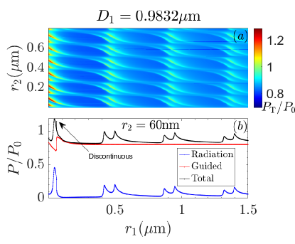
Here the total emission rate is no longer always continuous at the onset of a new guided mode. This can be seen in Fig. (17b), where spikes up for one data point exactly at the onset of a new guided mode, because the emission rate into radiation modes has not yet dropped. This is mostly likely due to numerical limitations and the exact transition point between radiation modes and guided modes would probably be problematic for any numerical algorithm99. The opposite can also occur, where drops as the emission rate into radiation modes drops just before the onset of a new guided mode. This issue is generally not a problem as is still continuous for most parameters, but using the analytical method exactly at the onset of new guided mode should be done with caution.
However, in the optimization of the factor the discontinuity of at the onset of new guided modes is problematic as this can lead to nonphysical peaks in the factor which the optimization procedure could locate. Therefore we have implemented two different kinds of constraints (see the next subsection) with the purpose of avoiding these points and used 2-3 optimization algorithms in MATLAB. The result is shown in Fig. (18). This does not lead to a completely smooth curve for the factor as for one ring, but we can confidently determine that within a limited interval the factor can be further increased.
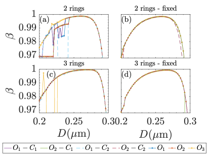
For most diameters, the different optimizations with and without constraints find the same value for the factor showing that the results are reliable. To construct Fig. (8), we have chosen the values which leads to smooth curves for the factor.
10.8 Optimization and constraints in the -factor optimization
In the -factor optimization we used three different optimization algorithms in MATLAB, namely fmincon107 (corresponding to in Fig. (18)), fminsearch108 () (more precisely fminsearch with boundaries109), and patternsearch110 (). For the first constraint, , we attempt to avoid the discontinuities in by first defining the following numerical derivatives:
| (76) |
| (77) |
| (78) |
| (79) |
where we have used and and corresponds to the parameters , or and so on. If either or then is artificially put to 0 such that the optimization avoids this point. The condition is then tested for all the parameters . In the second constraint, , we simply attempt to avoid all points where a new guided mode appears. Here we simply test if there is any difference in the number of guided modes within of all the parameters. If this is the case .
10.9 Additional simulations of the photonic nanowire
Here we will present the reflections and transmission coefficients of the photonic nanowire. First, we will optimize the reflection of the fundamental mode, , at the bottom mirror with respect to the silica layer thickness, , which can reduce the coupling to surface plasmons and radiation modes81, 82.
In Fig. (19) the reflection of the fundamental mode, , is shown as a function of the silica layer thickness, , for 0, 1, 2 and 3 rings. The silica layer thickness which provides the maximum reflection is close to for all numbers of rings. There is also a very slight increase in the maximum reflection as the numbers of rings increases, which is caused by the slightly increasing center diameter. The reflections at are: , , and , where the last sub index refers to the numbers of rings. The total reflection, , which includes scattering into radiation modes and any ring modes are: , , and showing that an insignificant amount of the fundamental mode is back-scattered into radiation. We have thus chosen .
In Fig. (20) the transmission coefficient with the Gaussian overlap, , is shown as a function of the taper angle, , for the different numbers of rings. The transmission coefficient is strongly dependent on the opening angle and so will the overall performance. For the smallest tapering angles, the transmission coefficient is almost the same for the different numbers of rings, which showcases that neither the increased diameter nor the rings decrease the transmission. The values obtained at with are: , , and . Around , the transmission is slightly better without any rings and then for the transmission is slightly better with the rings which is caused by the diameter change. To show the influence of the numerical aperture, we also plot the transmission coefficient as a function of the for 1 ring.
In Fig. (21), the transmission coefficient with the Gaussian overlap, , is shown for 1 ring as a function of the , for a few different tapering angles . In general, a larger increases the transmission coefficient and the same is true for the tapering angle. For large values of , decreasing the tapering angle further than does not increase the maximum transmission coefficient, but it does relax the requirement of the to obtain the maximum value.
With the decreased transmission coefficient, we expect an increased reflection at the top interface. The light can both be reflected back into the fundamental mode, but it can also be reflected back into radiation modes.
In Fig. (22), the reflection of the fundamental mode into itself, , and the total reflection of the fundamental mode, , is shown as a function of the tapering angle, , for the different numbers of rings. For tapering angles below , the reflection is very small, but already at the total reflection is around 0.03. Furthermore, most of the reflection is not into the fundamental mode itself, but into radiation modes and potentially ring modes. This also complicates the optimal values of and for the efficiency. Nonetheless, the reflection is very small for the lowest tapering angles.
In Fig. (23), the collection efficiency can vary up to 0.1 even when the tapering angle is only . This significantly benefits the structure without any rings as seen by comparing to the SMM. As such the effect of positioning the dipole dominates over the effect of the rings for larger tapering angles.
In Fig. (24), is shown as a function of the tapering angle, , for the different numbers of rings where and are chosen such that (a) is maximised and (b) is maximised. In Fig. (24a), is above 0.99 for any rings added and the value is close to the value for the infinite structures. even slightly exceeds 1 for 2 and 3 rings due to coupling between the evanescent modes and the fundamental mode, which indicates the breakdown of the SMM. For the structure without any rings, there is an increase in of at least 0.01 for all angles. If we then choose and such that is maximized as in Fig. (24b), then exceeds 1 for many tapering angles and even reaches 1.07 for 3 rings at . This is again due to a breakdown of the SMM which we have also reported in82 for the nanopost SPS. It also shows that maximizing and is not the same due to this breakdown. However, in the infinite structure is well-defined as a power ratio and as has already been shown is indeed useful when optimizing the collection efficiency.
10.10 Additional simulations of the Micropillar
In Fig. (25), we present the reproduced (a) factor, (b) , (c) , and (d) of Ref.17 as a function of the diameter, , for and top DBR layer pairs respectively. There are several peaks in the collection efficiency, both for and with values around . There are also several dips as described in the main text of the paper. At , we obtain and and this is one diameter for which we have chosen to add rings. At , we obtain and and this is the other diameter for which we have chosen to add rings.
In Fig. (26), (a) with , (b) with , (c) with , and (d) with are shown as a function of the air gap, , and the ring thickness, , for 2 rings with fixed parameters surrounding the structure. For , the pattern of and do agree very well with a slight deviation of the position for the maximum value. For , the agreement of the patterns is not as good, but still comparable. Ultimately, the collection efficiency can be increased from to at and and for from to at and .