Spin-valley locking for in-gap quantum dots in a MoS transistor
Abstract
Spins confined to atomically-thin semiconductors are being actively explored as quantum information carriers. In transition metal dichalcogenides (TMDCs), the hexagonal crystal lattice gives rise to an additional valley degree of freedom with spin-valley locking and potentially enhanced spin life- and coherence times. However, realizing well-separated single-particle levels, and achieving transparent electrical contact to address them has remained challenging. Here, we report well-defined spin states in a few-layer MoS2 transistor, characterized with a spectral resolution of eV at mK. Ground state magnetospectroscopy confirms a finite Berry-curvature induced coupling of spin and valley, reflected in a pronounced Zeeman anisotropy, with a large out-of-plane -factor of . A finite in-plane -factor () allows us to quantify spin-valley locking and estimate the spin-orbit splitting eV. The demonstration of spin-valley locking is an important milestone towards realizing spin-valley quantum bits.
I Introduction
Spins confined to semiconductor nanostructures have been investigated extensively for their potential to encode quantum bits (qubits) for quantum information processing Hanson and Awschalom (2008); Burkard et al. (2023). Atomically-thin semiconductors with hexagonal lattices Xu et al. (2014); Kormányos et al. (2014); Széchenyi et al. (2018); Pawłowski et al. (2021); Pawłowski (2019); Altıntaş et al. (2021), such as bilayer graphene Banszerus et al. (2021); Eich et al. (2018) and the transition metal dichalcogenides (TMDCs) Xu et al. (2014); Kormányos et al. (2014); Széchenyi et al. (2018); Pawłowski et al. (2021); Pawłowski (2019); Altıntaş et al. (2021), have recently attracted significant attention owing to their additional valley degree of freedom from non-equivalent conduction band minima at the and points (in graphene and TMDC monolayers) and and points (in TMDC multi-layers) of the Brillouin zone. TMDCs, in particular, offer strong spin-orbit coupling Kormányos et al. (2014) arising from the -orbitals of the heavy transition metal atom, and a large tunable bandgap Kormányos et al. (2014). In monolayers and odd-numbered multilayers, broken inversion symmetry combined with time-reversal symmetry can cause the spin and valley degrees to couple Xu et al. (2014) at both K (monolayers) and Q (odd multi-layers) points, promising novel approaches to controlling spin-valley states Kormányos et al. (2014); Széchenyi et al. (2018); Pawłowski et al. (2021); Altıntaş et al. (2021) with potentially enhanced spin life- and coherence times Pawłowski (2019); Pawłowski et al. (2021).
.
Consequently, there has been a significant effort to engineer TMDC-based quantum devices in which few or even single electronic charges and their spin can be isolated and controlled. Electrostatic confinement of electrons to quantum dots has so far been demonstrated in mono- and multi-layers of MoS2 Wang et al. (2018); Pisoni et al. (2018), WS2 Song et al. (2015), and WSe2 Davari et al. (2020); Boddison-Chouinard et al. (2021) and have shown clear signatures of Coulomb blockade in single-charge tunneling. Despite these significant advances in device engineering, however, it has remained challenging to isolate and address individual spin states in the few-electron regime Hanson et al. (2007) to confirm predictions of their spin-valley character in electron transport spectroscopy. In part, this challenge arises from poorly screened disorder potentials at extremely low carrier density near threshold Qiu et al. (2013); Jariwala et al. (2013), and a large electron effective mass Pisoni et al. (2018), dictating tight confinement potentials to within a few tens of nanometres Davari et al. (2020). Given these sizable challenges, only recently has transport through discrete energy levels been demonstrated in electrostatically defined TMDC quantum dots by Davari et al. Davari et al. (2020).
Different from electrostatically defined quantum dots, spins confined to atomic point defects or shallow dopants creating in-gap states Koenraad and Flatté (2011) have proven Fuechsle et al. (2012); Weber et al. (2014) to provide tight confinement that is robust to disorder and yields well-separated single-particle levels with energy splitting of up to several meV Fuechsle et al. (2012); Weber et al. (2014). In-gap states have also been observed in TMDC-based quantum devices Papadopoulos et al. (2020); Devidas et al. (2021). However, detailed investigations Zeeman anisotropy for different directions of the applied magnetic field, allowing to infer information on spin-valley character, have so far been missing.
Resolving individual spin states and probing subtle changes in their state energy from applied electric or magnetic fields requires spectral resolution near the thermal limit (). Yet, in-gap states are usually confined near or below threshold in semiconductor devices. In this extremely low carrier-density regime, it has remained challenging to form transparent electrical contacts Wang and Chhowalla (2022), which stay Ohmic down to the required milliKelvin temperatures.
Here, we overcome this problem by the use of gate-tunable contacts, allowing us to perform transport spectroscopy with a resolution limited only by the electronic temperature of the reservoirs ( mK). Our detailed ground state magnetospectroscopy in vectorized magnetic fields confirms a pronounced Zeeman anisotropy with effective out-of-plane -factor as large as , consistent with spin-valley locking. We attribute a small but finite effective in-plane -factor () to inter-valley scattering in the presence of the defect potential, allowing us to estimate a spin-orbit splitting for electrons (100eV).
II Results and Discussion
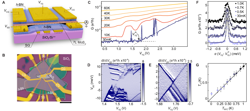
Figure 1A-B shows the schematic of our MoS2 transistor device alongside a false-colored optical microscope image. A seven atomic layers () thick MoS2 crystal (see supporting information) was encapsulated between two hexagonal boron nitride (-BN) layers and contacted with Ti/Au source (S) and drain (D) electrodes. We use a separate metal top gate (TG) and contact gates (CG) to independently tune the electron density in the TMDC transistor channel near threshold, while maintaining a high carrier density within the contact regions. A set of local gate electrodes (SG), not used for the work presented, were left floating.
Transfer curves measured at different temperatures are plotted in Figure 1C, showing the typical -type behaviour expected for natural MoS2, in which doping arises from native point defects such as chalcogen (S) vacancies Qiu et al. (2013); Hong et al. (2015). Near and below threshold (1.78 V), we observe a series of sharp conductance resonances consistent with Coulomb blockade (CB) in single-charge tunneling. The finite conductance observed sub-threshold at higher temperatures can be shown (see supporting information) to arise from 2D variable range hopping Qiu et al. (2013); Jariwala et al. (2013) within impurity bands, consistent with shallow -type doping. Bias spectroscopy (Figure 1D) confirms signatures of stochastic Coulomb blockade Chuang et al. (2012), with the detailed pattern of charge transitions in number and position varying from cool-down to cool-down. Conductance peaks near or above threshold have previously been attributed to point defect ensembles and/or disorder potentials affecting the conduction band tail Papadopoulos et al. (2020); Devidas et al. (2021); Ramezani et al. (2021); Kotekar-Patil et al. (2019). Sub-threshold peaks observed, however, may only be explained by tunneling through impurity-bound states within the bandgap Papadopoulos et al. (2020); Devidas et al. (2021).
As shown by the high-resolution close-ups in Figure 1D-E, measured in an initial cool-down of the device, we observe single-electron tunneling through small clusters of in-gap states. However, we can also locate isolated charge transitions (Figure 1E), which will be the focus of our investigation. For the transition shown, symmetric slopes bounding the Coulomb diamond indicate an approximately equal capacitive coupling to source and drain reservoirs. Multiple resonances with splitting of order meV, parallel to the diamond edges are seen, which can have a number of origins. At positive bias, we observe a single resonance above the ground state with splitting 300 eV which may reflect a low-lying spin- or orbital excited state. Above, we observe a large gap in the excitation spectrum of at least 10 meV (see supplementary information Figure. S4). Assuming a lower limit of the orbital splitting 10 meV we estimate the radius of the dot to be at most between 1.88 nm to 4.1 nm, depending on whether a 2D/3D dot or K/Q valleys are considered. These values are of similar order as what has been observed for S-vacancies in STM measurements Vancsó et al. (2016), confirming the atomic scale confinement of electrons in this device. Multiple parallel resonances at negative bias, with non-uniform spacing likely reflect a combination of excited states with features arising from a non-uniform reservoir density-of-states (DOS) Papadopoulos et al. (2020). The asymmetry in bias observed may suggest an asymmetry in the tunnel coupling to source and drain reservoirs Escott et al. (2010).
An estimate of the effective temperature in the S and D electron reservoirs – and hence our spectral resolution – can be obtained by fitting the Coulomb peaks Foxman et al. (1993) measured at a small bias of 0.01 mV, as shown in Figure 1F (see supporting information for detail). Our fits confirm that tunneling proceeds through individual quantized energy levels Beenakker (1991); Song et al. (2015) rather than through a many-electron island in the classical regime Kotekar-Patil et al. (2019), as evident from the approximately linear increase in the peak resistance with temperature (see supplementary information). We extract mK at the base temperature of our dilution refrigerator – the lowest reported for Coulomb blockade signatures in TMDC materials to date. The corresponding thermal broadening eV, together with a finite lifetime broadening eV, sets the limit of our spectral resolution and attests to the quality of our contacts.
.
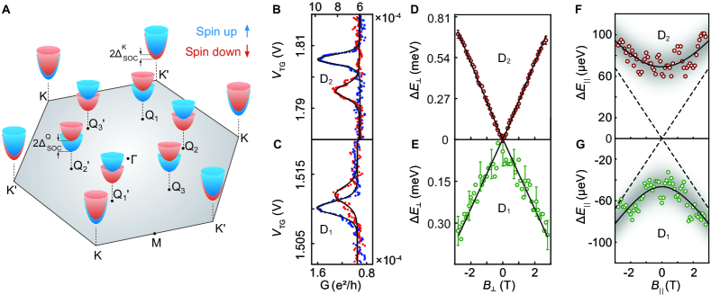
Detailed insight into the interplay of spin and valley can be gained from ground state magnetospectroscopy and measurement of the Zeeman anisotropy, as presented in Figure 2,3. In MoS2 multi-layers the conduction band (CB) if formed by degenerate minima at both the K- and the Q-points of the Brillouin Zone as shown in Figure 2A. For 7L crystals (see supplementary information), the CB minima is at Q-points followed by a mixing of K-points 137 meV above as confirmed from our DFT calculations. Shallow impurities such as sulphur vacancies can draw states from either conduction band pocket. In both TMDC monolayers and odd numbered multilayers broken inversion symmetry lifts the degeneracy of the valleys, split by 2 due to the intrinsic spin-orbit coupling Kormányos et al. (2014). This gives rise to a non-zero Berry curvature of opposite sign in the respective Q/Q′ and K/K′ valleys, which acts like effective magnetic field in momentum space, giving rise to a valley magnetic moment, oriented perpendicular to the MoS2 plane Xu et al. (2014); Schaibley et al. (2016). In addition, the spin-orbit coupling acts as an effective out-of-plane magnetic field, polarizing spins perpendicular to the MoS2 crystal plane, ideally lacking an in-plane magnetic moment. Time-reversal symmetry dictates the spin splitting to have opposite sign at the K/K′ and Q/Q′ valleys, giving rise to an effective coupling between spin and valley pseudospin. Regardless of the valley occupation, given the spin texture in odd-numbered multilayers of MoS2, spins are therefore expected to be locked to the out-of-plane direction with a vanishing Zeeman energy for in-plane magnetic fields. Observation of a pronounced Zeeman anisotropy is thus a clear sign of spin-valley locking. Indeed, spin-valley coupling of extended conduction band states at has been reported to dominate electron transport in odd-number multi-layers (trilayer and above) of MoS2 Wu et al. (2016); Roldán et al. (2014). In trilayer MoS2, claims for both -valley Pisoni et al. (2017) and -valley Masseroni et al. (2021) transport have been made. However, the spin-valley nature of impurity bound states as evident from Zeeman anisotropy measurements has not yet been explored.
When a time-reversal symmetry breaking magnetic field is applied, the total Zeeman correction can be written as
| (1) |
| (2) |
where is the effective out-of-plane -factor, which can be expressed as a combination of spin () and valley () -factors, in which the valley () and spin () quantum numbers can take the values by for {, } and for {, }. is the effective in-plane -factor. is the inversion symmetry breaking term which can arise from a combination of spin-orbit coupling () and inter-valley mixing . comprises of both and components, whereas consists of a component. Therefore, is added quadratically for fields, while is added quadratically in the case of and linearly in the case of fields. This model is applicable to any unpaired valence spin states with spin-valley locking, without assumptions regarding charge occupation, shell filling sequence, or specific spin- and valley- g-factors, thus allowing the estimation of spin-orbit coupling strength through effective g-factor measurements. Figure 2B-E confirms Zeeman-shifted spin-valley ground states, measured for two charge transitions, and , in an out-of-plane magnetic field, both measured in a second cool-down of the device (see supplementary information Fig.S4). For the out-of-plane Zeeman term (Eq. 1), the addition of a small constitutes a constant offset to the Zeeman term, i.e. with no change in slope and hence . From fits to a linear Zeeman field, we extract out-of-plane effective -factors = () and = (), respectively, where we have assumed gate levers of meV/V and meV/V, extracted from the slope of the CB diamonds (see supporting Information).
Ideally, the out-of-plane polarized spins in odd-layered TMDCs are expected to couple weakly to any in-plane magnetic fields. However a small but finite Zeeman shift in -fields can be detected as shown in Figure 2F,G. The dashed black lines indicate the corresponding Zeeman slope for 0. Taking into account an inversion symmetry-breaking term in Eq. 2, we can fit the data (solid black line in Fig. 2F-G). The term gives rise to departure from a linear in-plane Zeeman shift at low . At 2 T the in-plane field is strong enough to cant the spins into the MoS2 crystal plane giving rise to a linear Zeeman shift for fields above. From fits to Eq. (2), we extract for both transitions. It also allows us to extract eV () and eV (), just within the spectral resolution limit of our measurement (eV at 150 mK), and of similar magnitude as the low lying excited state at positive bias observed in Figure. 1E. Although, there could be other sources of symmetry-breaking, such as Rashba spin-orbit coupling from field-effect gating, it is expected to be non-negligible only in aggressively gated devices, for example, dual-gated or devices with ionic liquid gating Piatti et al. (2018). Since here, the transitions measured are sub-threshold, at low top-gate voltages, we expect such effects to play a minor role in our device.
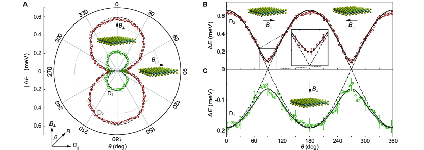
We confirm the notion of a pronounced Zeeman anisotropy in Figure 3A, measured at T for both D1 and D2, demonstrating near-vanishing Zeeman shifts for in-plane magnetic fields at angles ° and 270° from the surface normal. Reasonable fits can indeed be obtained by assuming (dashed black lines in Figure 3A), assuming that magnetic moments are strictly spin-valley locked out-of-plane. These fits also allows us to determine the reference point where , that is, where the out-of-plane Zeeman field vanishes in the absence of an in-plane -factor (compare dashed lines in Figure 3B-C).
Out-of-plane Zeeman shifts have been demonstrated Papadopoulos et al. (2020); Davari et al. (2020), in transport through both defects Papadopoulos et al. (2020) and electrostatically-defined quantum dots Davari et al. (2020), reporting out-of-plane -factors ranging from 3.4-15.8 Papadopoulos et al. (2020) and 0.8-2.4 Davari et al. (2020), respectively. While we cannot fully exclude the possibility that the out-of-plane -factor of could represent a pure spin state without any valley-Zeeman contribution Tsunetomo et al. (2021), the large -factor observed for , and the pronounced -factor anisotropy observed in both transitions can only be explained by a combination of spin and valley Zeeman effects. Further extracting the respective contributions of spin- and valley -factors to the total effective -factor would require knowledge of the precise charge occupation and spin-valley eigenspectrum, neither of which are known with certainty. Although an orbital magnetic moment could in principle contribute to the overall enhancement of the -factor Davari et al. (2020), we expect them to play a minor role in the atomically confined spin states Pryor and Flatté (2006) considered here.
Consistent can also be confirmed directly from Zeeman shifts of the ground state transition for D1 and D2 as a function of magnetic field orientation (), as summarized in Figure 3B-C. The dashed black lines in Figure 3B-C are the same out-of-plane Zeeman fits as determined earlier in Figure 3A, scaled by the lever arms, assuming . In this representation, the fits are seen to clearly underestimate the measured data at in-plane angles and for which a finite in-plane Zeeman shift is present. A better fit to the data, including the pronounced rounding at the minima, can be obtained by considering a finite in-plane -factor such that
As shown by the solid black lines, fits to Eq. (LABEL:Eani) allow us to confirm comparable values, (), (), (), and () for the two transitions, in agreement with those extracted from the in-plane Zeeman shifts in Figure 2F-G. We note that contributions from in Eq. (LABEL:Eani) are not detectable within the fit quality, since the measurement was taken at a large enough magnetic field magnitude 2.8 T, at which the Zeeman shifts are nearly linear in both in-plane and out-of-plane magnetic fields. The rounding at the minima therefore arises purely from the presence of a finite in-plane -factor.
A finite in-plane -factor as observed can indeed be expected to arise from valley-mixing in the presence of an abrupt defect potential Széchenyi et al. (2018),
| (4) |
As seen from the expression above, is expressed through the ratio of inter-valley scattering and SOC splitting and can hence be used to quantify the degree of spin-valley locking. For , an isotropic spin -factor would be expected. However, if scattering between valleys is negligible (), electron spin is locked to a well-defined valley degree of freedom and is recovered. Here, we encounter an intermediate scenario where a pronounced -factor anisotropy represents spin-valley locking, but a finite in-plane -factor arises from inter-valley scattering.
In monolayers of MoS2, upper limits to of 150 eV and 1.5 meV have been predicted Széchenyi et al. (2018) for S and Mo vacancies, respectively. Considering also the predicted spin-orbit splitting meV for the conduction band in monolayers Kormányos et al. (2014), as well as predicted by theory Kormányos et al. (2014), we expect for S vacancies, while a nearly isotropic would be expected for Mo vacancies. Although both estimates are likely to be modified in multi-layers, their ratio agrees reasonably well with that expected for S vacancies. While we cannot fully eliminate the role of disorder potentials in confining individual spins, S-vacancies are likely candidates given that they are prevalent in natural MoS2 crystals Tumino et al. (2020); Hong et al. (2015), and are known as shallow -type dopants Qiu et al. (2013); Schuler et al. (2019). Strong -type behaviour is indeed reflected in the transfer curves of our device, with in-gap states observed close to the conduction band edge (Figure 1C), similar to the case of shallow donors in covalent semiconductors such as silicon or GaAs. Thus, we expect the defect wave function to inherit the characteristics of the conduction band electronic structure Kohn and Luttinger (1955). The relatively large ratio of spin-orbit coupling to inter-valley scattering inferred from our experiments further indicates that the spin-orbit energy scale dominates the sum of their squares , allowing us to estimate eV. Although low compared to calculations Kormányos et al. (2014) and measurements in monolayers Marinov et al. (2017), this value possibly reflects the reduced SOC strength expected in strongly confined in-gap states and in multi-layers Chang et al. (2014). Further suppression of the SOC gap has also been predicted for quantum dots with reduced radius Bieniek et al. (2020), similar to what would be expected in highly-confined in-gap wave functions, but different from the soft confinement potentials encountered in electrostatically defined quantum dots of larger radii. It is hard to predict what would be expected for defect-bound spin-valley states in MoS2.
We note that in bilayer graphene Eich et al. (2018); Banszerus et al. (2021), similar spin-valley locked ground states have recently allowed the demonstration of valley Zeeman splittings with -factors as large as Lee et al. (2020), and with a spin-orbit gap of eV Banszerus et al. (2021). The larger spin-valley splitting due to stronger SOC achievable in MoS2 monolayers, however, gives rise to the strong suppression of in-plane magnetic moments in mono- and odd-layered MoS2, different from the case of graphene in which has been reported Eich et al. (2018). An aspect to consider for future work is to investigate the role of gate tunable spin-orbit coupling, similar to what has recently been demonstrated for quantum point contacts in bilayer graphene Banszerus et al. (2020).
III Conclusion
To conclude, we have demonstrated single-electron tunneling through in-gap states near threshold of a few-layer MoS2 transistor. From sensitive ground state magnetospectroscopy near the thermal resolution limit, we confirm spin-valley locking of well-defined spin states as detected from a pronounced anisotropy of the Zeeman splitting in vectorized magnetic fields. The finite in-plane -factor observed has allowed us to extract an estimate for the spin-orbit splitting in the conduction band of order eV. The observation of spin-valley locking resolved via the Zeeman anisotropy of well-defined spin states in a MoS2 transistor device for the first time is an important milestone towards determining spin life- Weber et al. (2018) and coherence Pla et al. (2012) times in TMDC-based spin-valley quantum bits.
IV Acknowledgements
This research is supported by the National Research Foundation (NRF) Singapore, under the Competitive Research Programme “Towards On-Chip Topological Quantum Devices” (NRF-CRP21-2018-0001), with further support from the Singapore Ministry of Education (MOE) Academic Research Fund Tier 3 grant (MOE2018-T3-1-002) “Geometrical Quantum Materials”. BW acknowledges a Singapore National Research Foundation (NRF) Fellowship (NRF-NRFF2017-11). The device fabrication in the work was carried out at the Micro and Nano-Fabrication Facility (MNFF), Centre of Advanced 2D Materials (CA2DM) at the National University of Singapore.
V Author Contributions
RK and SB contributed equally to this work. RK carried out the device nanofabrication. SB performed the electrical measurements with the help of RK. RK, SB, and BW analyzed the data with input by YH and RR on crystal symmetry and -factor anisotropy. HM performed the DFT calculations. BW perceived and coordinated the project. RK, SB, and BW wrote the manuscript with input from all authors.
References
- Hanson and Awschalom (2008) R. Hanson and D. D. Awschalom, Nature 453, 1043 (2008).
- Burkard et al. (2023) G. Burkard, T. D. Ladd, A. Pan, J. M. Nichol, and J. R. Petta, Reviews of Modern Physics 95, 025003 (2023), URL https://doi.org/10.1103/revmodphys.95.025003.
- Xu et al. (2014) X. Xu, W. Yao, D. Xiao, and T. F. Heinz, Nature Physics 10, 343 (2014).
- Kormányos et al. (2014) A. Kormányos, V. Zólyomi, N. D. Drummond, and G. Burkard, Physical Review X 4, 011034 (2014).
- Széchenyi et al. (2018) G. Széchenyi, L. Chirolli, and A. Pályi, 2D Materials 5, 035004 (2018).
- Pawłowski et al. (2021) J. Pawłowski, M. Bieniek, and T. Woźniak, Physical Review Applied 15, 054025 (2021).
- Pawłowski (2019) J. Pawłowski, New Journal of Physics 21, 123029 (2019).
- Altıntaş et al. (2021) A. Altıntaş, M. Bieniek, A. Dusko, M. Korkusiński, J. Pawłowski, and P. Hawrylak, Physical Review B 104, 195412 (2021).
- Banszerus et al. (2021) L. Banszerus, S. Möller, C. Steiner, E. Icking, S. Trellenkamp, F. Lentz, K. Watanabe, T. Taniguchi, C. Volk, and C. Stampfer, Nature Communications 12, 1 (2021).
- Eich et al. (2018) M. Eich, F. Herman, R. Pisoni, H. Overweg, A. Kurzmann, Y. Lee, P. Rickhaus, K. Watanabe, T. Taniguchi, M. Sigrist, et al., Physical Review X 8, 031023 (2018).
- Wang et al. (2018) K. Wang, K. De Greve, L. A. Jauregui, A. Sushko, A. High, Y. Zhou, G. Scuri, T. Taniguchi, K. Watanabe, M. D. Lukin, et al., Nature Nanotechnology 13, 128 (2018).
- Pisoni et al. (2018) R. Pisoni, Z. Lei, P. Back, M. Eich, H. Overweg, Y. Lee, K. Watanabe, T. Taniguchi, T. Ihn, and K. Ensslin, Applied Physics Letters 112, 123101 (2018).
- Song et al. (2015) X.-X. Song, Z.-Z. Zhang, J. You, D. Liu, H.-O. Li, G. Cao, M. Xiao, and G.-P. Guo, Scientific Reports 5, 1 (2015).
- Davari et al. (2020) S. Davari, J. Stacy, A. Mercado, J. Tull, R. Basnet, K. Pandey, K. Watanabe, T. Taniguchi, J. Hu, and H. Churchill, Physical Review Applied 13, 054058 (2020).
- Boddison-Chouinard et al. (2021) J. Boddison-Chouinard, A. Bogan, N. Fong, K. Watanabe, T. Taniguchi, S. Studenikin, A. Sachrajda, M. Korkusinski, A. Altintas, M. Bieniek, et al., Applied Physics Letters 119, 133104 (2021).
- Hanson et al. (2007) R. Hanson, L. P. Kouwenhoven, J. R. Petta, S. Tarucha, and L. M. Vandersypen, Reviews of Modern Physics 79, 1217 (2007).
- Qiu et al. (2013) H. Qiu, T. Xu, Z. Wang, W. Ren, H. Nan, Z. Ni, Q. Chen, S. Yuan, F. Miao, F. Song, et al., Nature Communications 4, 1 (2013).
- Jariwala et al. (2013) D. Jariwala, V. K. Sangwan, D. J. Late, J. E. Johns, V. P. Dravid, T. J. Marks, L. J. Lauhon, and M. C. Hersam, Applied Physics Letters 102, 173107 (2013).
- Koenraad and Flatté (2011) P. M. Koenraad and M. E. Flatté, Nature Materials 10, 91 (2011).
- Fuechsle et al. (2012) M. Fuechsle, J. A. Miwa, S. Mahapatra, H. Ryu, S. Lee, O. Warschkow, L. C. Hollenberg, G. Klimeck, and M. Y. Simmons, Nature Nanotechnology 7, 242 (2012).
- Weber et al. (2014) B. Weber, Y. M. Tan, S. Mahapatra, T. F. Watson, H. Ryu, R. Rahman, L. C. Hollenberg, G. Klimeck, and M. Y. Simmons, Nature Nanotechnology 9, 430 (2014).
- Papadopoulos et al. (2020) N. Papadopoulos, P. Gehring, K. Watanabe, T. Taniguchi, H. S. Van Der Zant, and G. A. Steele, Physical Review B 101, 165303 (2020).
- Devidas et al. (2021) T. Devidas, I. Keren, and H. Steinberg, Nano Letters 21, 6931 (2021).
- Wang and Chhowalla (2022) Y. Wang and M. Chhowalla, Nature Reviews Physics 4, 101 (2022).
- Hong et al. (2015) J. Hong, Z. Hu, M. Probert, K. Li, D. Lv, X. Yang, L. Gu, N. Mao, Q. Feng, L. Xie, et al., Nature Communications 6, 1 (2015).
- Chuang et al. (2012) C. Chuang, R. K. Puddy, M. R. Connolly, S.-T. Lo, H.-D. Lin, T.-M. Chen, C. G. Smith, and C.-T. Liang, Nanoscale Research Letters 7, 1 (2012), URL https://doi.org/10.1186/1556-276x-7-459.
- Ramezani et al. (2021) M. Ramezani, I. C. Sampaio, K. Watanabe, T. Taniguchi, C. Schonenberger, and A. Baumgartner, Nano Letters 21, 5614 (2021).
- Kotekar-Patil et al. (2019) D. Kotekar-Patil, J. Deng, S. L. Wong, and K. E. J. Goh, ACS Applied Electronic Materials 1, 2202 (2019).
- Vancsó et al. (2016) P. Vancsó, G. Z. Magda, J. Pető, J.-Y. Noh, Y.-S. Kim, C. Hwang, L. P. Biró, and L. Tapasztó, Scientific Reports 6, 1 (2016).
- Escott et al. (2010) C. C. Escott, F. A. Zwanenburg, and A. Morello, Nanotechnology 21, 274018 (2010).
- Foxman et al. (1993) E. Foxman, P. McEuen, U. Meirav, N. S. Wingreen, Y. Meir, P. A. Belk, N. Belk, M. Kastner, and S. Wind, Physical Review B 47, 10020 (1993).
- Beenakker (1991) C. W. Beenakker, Physical Review B 44, 1646 (1991).
- Schaibley et al. (2016) J. R. Schaibley, H. Yu, G. Clark, P. Rivera, J. S. Ross, K. L. Seyler, W. Yao, and X. Xu, Nature Reviews Materials 1, 16055 (2016).
- Wu et al. (2016) Z. Wu, S. Xu, H. Lu, A. Khamoshi, G.-B. Liu, T. Han, Y. Wu, J. Lin, G. Long, Y. He, et al., Nature Communications 7, 1 (2016).
- Roldán et al. (2014) R. Roldán, J. A. Silva-Guillén, M. P. López-Sancho, F. Guinea, E. Cappelluti, and P. Ordejón, Annalen der Physik 526, 347 (2014).
- Pisoni et al. (2017) R. Pisoni, Y. Lee, H. Overweg, M. Eich, P. Simonet, K. Watanabe, T. Taniguchi, R. Gorbachev, T. Ihn, and K. Ensslin, Nano Letters 17, 5008 (2017).
- Masseroni et al. (2021) M. Masseroni, T. Davatz, R. Pisoni, F. K. de Vries, P. Rickhaus, T. Taniguchi, K. Watanabe, V. Falko, T. Ihn, and K. Ensslin, Physical Review Research 3, 023047 (2021).
- Piatti et al. (2018) E. Piatti, D. De Fazio, D. Daghero, S. R. Tamalampudi, D. Yoon, A. C. Ferrari, and R. S. Gonnelli, Nano letters 18, 4821 (2018).
- Tsunetomo et al. (2021) N. Tsunetomo, S. Iguchi, M. Wierzbowska, A. Ueda, Y. Won, S. Heo, Y. Jeong, Y. Wakayama, and K. Marumoto, Communications Materials 2, 1 (2021).
- Pryor and Flatté (2006) C. E. Pryor and M. E. Flatté, Physical Review Letters 96, 026804 (2006).
- Tumino et al. (2020) F. Tumino, C. S. Casari, A. Li Bassi, and S. Tosoni, The Journal of Physical Chemistry C 124, 12424 (2020).
- Schuler et al. (2019) B. Schuler, D. Y. Qiu, S. Refaely-Abramson, C. Kastl, C. T. Chen, S. Barja, R. J. Koch, D. F. Ogletree, S. Aloni, A. M. Schwartzberg, et al., Physical Review Letters 123, 076801 (2019).
- Kohn and Luttinger (1955) W. Kohn and J. M. Luttinger, Phys. Rev. 98, 915 (1955).
- Marinov et al. (2017) K. Marinov, A. Avsar, K. Watanabe, T. Taniguchi, and A. Kis, Nature Communications 8, 1 (2017).
- Chang et al. (2014) T.-R. Chang, H. Lin, H.-T. Jeng, and A. Bansil, Scientific Reports 4, 1 (2014).
- Bieniek et al. (2020) M. Bieniek, L. Szulakowska, and P. Hawrylak, Physical Review B 101, 035401 (2020).
- Lee et al. (2020) Y. Lee, A. Knothe, H. Overweg, M. Eich, C. Gold, A. Kurzmann, V. Klasovika, T. Taniguchi, K. Wantanabe, V. Falko, et al., Physical Review Letters 124, 126802 (2020).
- Banszerus et al. (2020) L. Banszerus, B. Frohn, T. Fabian, S. Somanchi, A. Epping, M. Müller, D. Neumaier, K. Watanabe, T. Taniguchi, F. Libisch, et al., Physical review letters 124, 177701 (2020).
- Weber et al. (2018) B. Weber, Y.-L. Hsueh, T. F. Watson, R. Li, A. R. Hamilton, L. C. Hollenberg, R. Rahman, and M. Y. Simmons, npj Quantum Information 4, 1 (2018).
- Pla et al. (2012) J. J. Pla, K. Y. Tan, J. P. Dehollain, W. H. Lim, J. J. Morton, D. N. Jamieson, A. S. Dzurak, and A. Morello, Nature 489, 541 (2012).