Voltage deficit in solar cells with suppressed recombination
Abstract
The observed open circuit voltages in best performing solar cells are explained outside of the recombination paradigm, based on such factors as electrostatic screening, Meyer - Neldel effect, and lateral nonuniformities. The underlying concept of suppressed recombination presents a long neglected alternative pathway to efficient PV. The criterion of suppressed recombination is consistent with the data for best performing solar cells. Also, consistent with the observations, is the open circuit voltage deficit that exhibits a lower bound of about V, does not correlate well with the optical gap, and shows a significant dispersion for materials possessing the same gap values.
I Introduction
The many year quest for photovoltaic (PV) efficiency brought in significant improvements on many fronts. [1, 2] The understanding of PV operations evolved as well through improved modeling and new concepts. [3, 4, 5, 6, 7] Through all the underlying developments, one paradigm remaining intact was that of defect mediated nonradiative recombination [commonly termed Shockley-Read-Hall (SRH) [8, 9, 10, 11]] dominating PV efficiency. [3, 4, 5, 6] Indeed, we are aware of just one publication addressing an alternative limitation due to the charge carriers extraction. [12]
A recent push towards an alternative explanation of the efficiency limitations was related to the case of PV with suppressed recombination [13] and based on the following approach. (i) Assume that there is no recombination, i. e. the rate of electron-hole pair generation equals the number of photons absorbed per time. In other words, we assume zero photocurrent loss. (ii) Extract the optimum power voltage of a PV cell from its current-voltage characteristic, i. e. is treated as an empirical parameter. The product presents the device power, which yields the efficiency. How good is the above assumption of zero recombination in electric current? The comparison of best cell efficiencies [1, 2] with calculations [13] validate that assumption to high accuracy.
Given a negligible effect of recombination on current, it is natural to expect its similarly weak effect on device voltage thus questioning the role of SRH recombination altogether. There is however an alternative hypothesis claiming a significant deficit (loss) of PV voltages and relating it to recombination either directly or defined vaguely in terms of ‘material quality’ exhibiting itself e. g. in Urbach tails [14, 15, 16, 17, 18, 19, 20, 21, 22, 23, 24, 25, 26, 27]. More specifically, the open circuit voltage () deficit is defined as
| (1) |
The hypothesis behind the definition of Eq. (1) is that is limited to the built-in voltage , which, in turn, is bound to the optical gap .
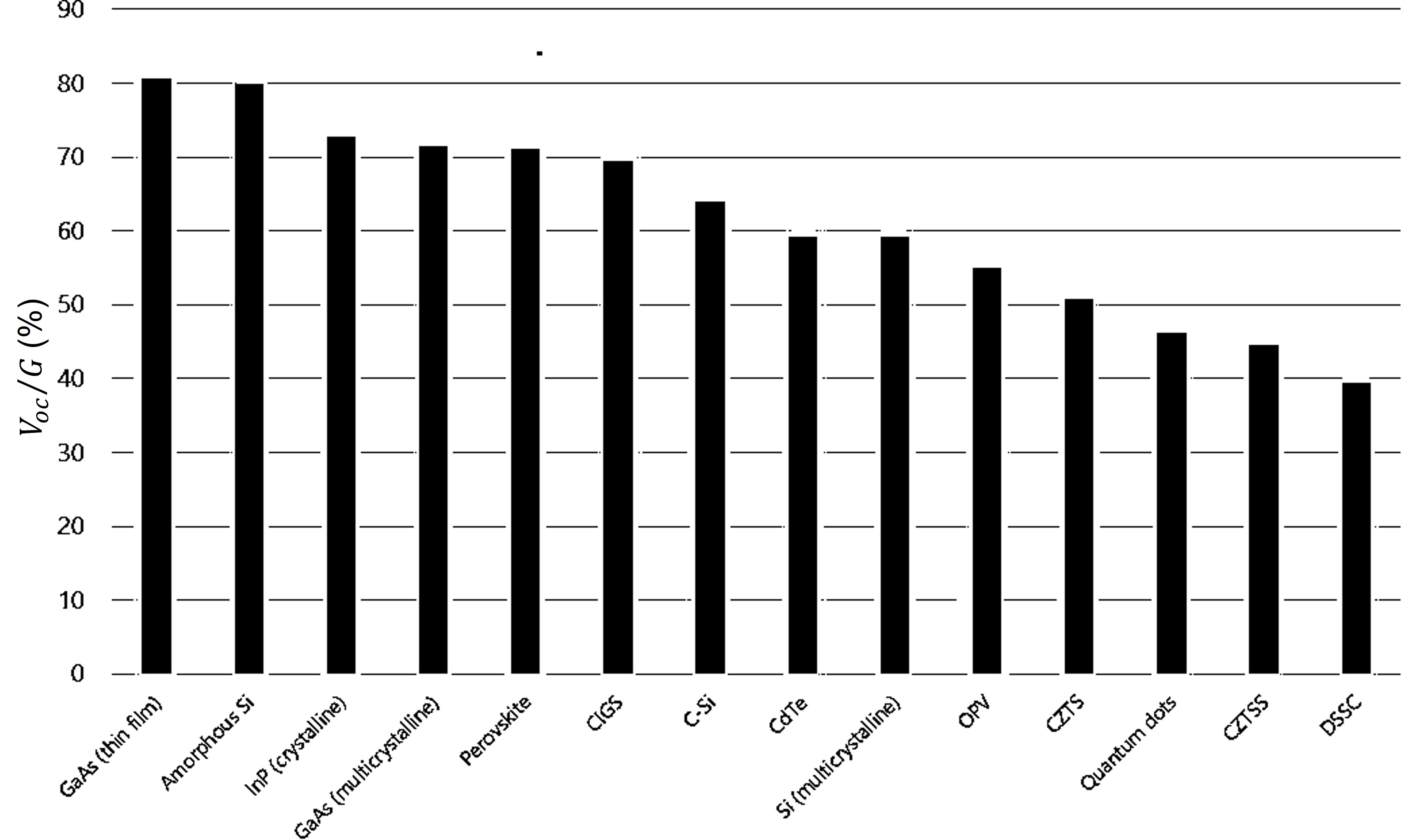
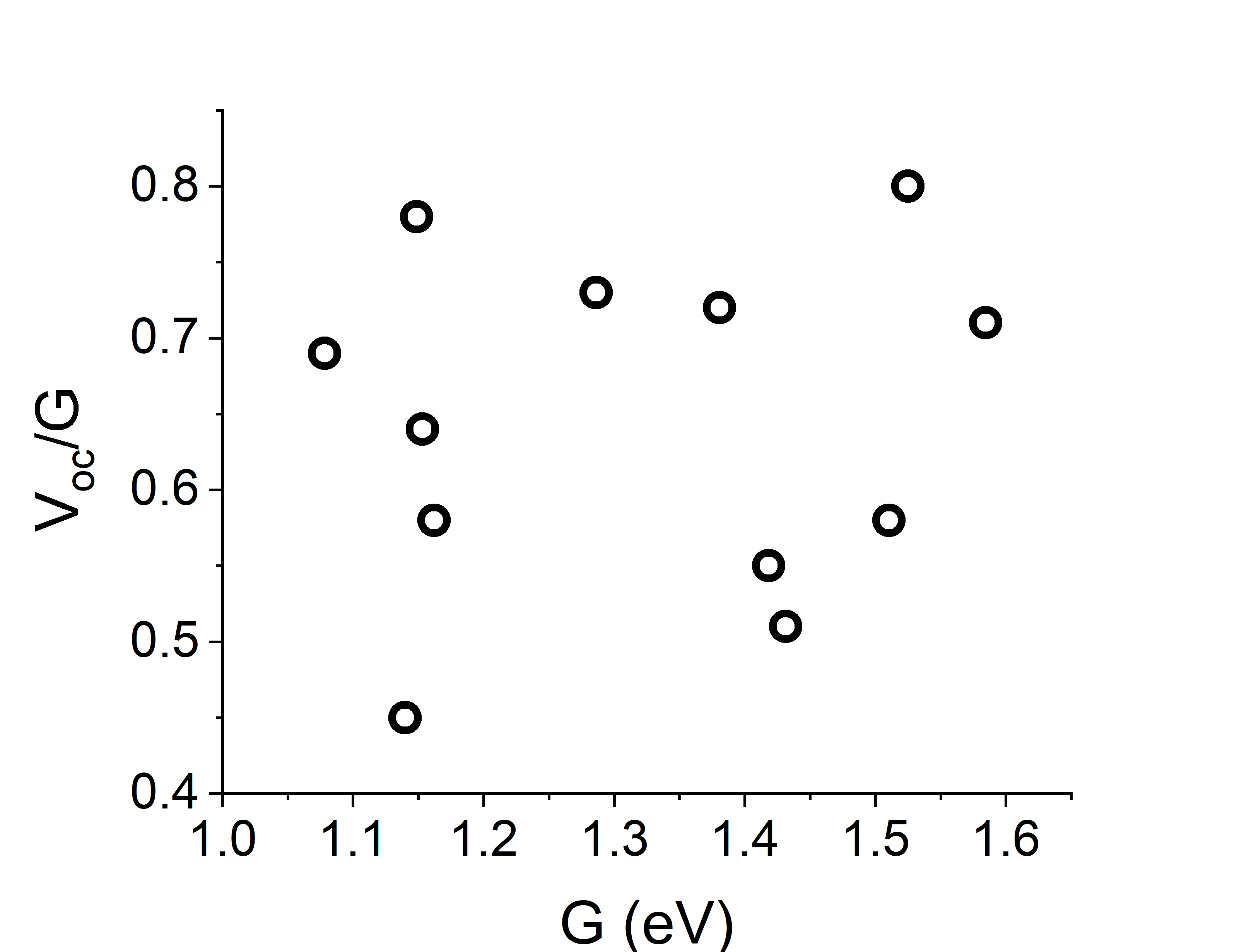
The available data in Fig. 1 shows, at the first glance, a certain correlation, until we recognize that the horizontal axis is not quantified. Assigning the gap values to the materials leads to the data summarized in Table 1 and in Fig. 2, which totally destroy the correlation.
| Brand | (V) | G (eV) | Brand | (V) | (eV) |
| GaAs TF | 1.22 | 1.53 | c-Si | 0.738 | 1.115 |
| a-Si | 0.896 | 1.14 | CdTe | 0.876 | 1.51 |
| InP | 0.939 | 1.286 | Si mc | 0.674 | 1.16 |
| GaAs - mc | 0.994 | 1.38 | OPV | 0.78 | 1.42 |
| Perovs | 1.125 | 1.585 | CZTS | 0.73 | 1.43 |
| CIGS | 0.744 | 1.078 | CZTSS | 0.513 | 1.14 |
To set aside the role of recombination, we consider then the case of PV with suppressed recombination. That study revealed several voltage affecting factors not related to recombination and calling upon certain practical remedies of minimizing the voltage deficit and improving PV efficiency. Simultaneously we will derive the criterion of suppressed recombination showing that it holds well for at least best thin-film PV.
II Nonradiative recombination: sufficient vs necessary
The PV literature is swarming with recombination topics showing how recombination dominated losses form sufficient basis for PV understanding. The later sufficiency means that SRH recombination theory [8, 9, 10, 11] with adjustable defect parameters enables one to satisfactory interpret the data. However, sufficiency alone does not prove the causal relationship between recombination and performance. A necessity must be established in parallel where one condition (recombination) must be present in order for another one (performance) to occur. Based on our extensive literature search, the assertion of recombination necessity is rarely, if at all, addressed. Indeed, such assertion would entail a formidable task of showing how the observed performance cannot be understood without the assumption of recombination loss.
Here, we proceed along an alternative logical pathway showing how the observed performance can be explained without the notion of recombination. Should the latter be the case, recombination will lack the significance of general necessity giving a way to the paradigm of suppressed recombination PV. That paradigm does not imply zero recombination, but rather a recombination that is not as dominant as previously believed. Our evidence against the general necessity of recombination in PV is as follows.
-
1.
The physical processes underlying the recombination and drift processes are quite different, [7, 34] and so are their corresponding characteristic times. Therefore, it is natural to expect, in general, strong inequalities between the recombination time and drift time : either (recombination practically irrelevant: the carriers leave the sample sooner) or (recombination totally dominates the PV efficiency). The possibility of recombination just moderately affecting efficiency, say, as often assumed, by 1-10 relative percent, i. e. would be a sheer coincidence. In particular, it is reasonable to expect that recombination is irrelevant for the best PV at least.
-
2.
Experimental data covering a variety of semiconductors exhibit the characteristic recombination times in the domain from microseconds to milliseconds, [29, 30, 31, 32, 33, 34, 35, 36] much longer than the characteristic drift times ns for thin film PV. [7] For high quality materials,such as crystalline Si, the inequality can hold even when represents the diffusion rather than drift time and device thickness reaches 100 m.
-
3.
The above mentioned recent publication [13] showing that totally neglecting recombination loss in the electric current yields rather accurate predictions for the observed PV efficiencies. Note that the latter argument is limited to the best performing cells. Our analysis in what follows will inherit the same limitation. (It is obvious indeed that low quality cells can suffer of strong recombination.)
The suppressed recombination concept significantly simplifies PV description, eliminates the need in multiple adjustable parameters, and shifts attention from the defect chemistry to basic physics. Surprisingly, that concept has never been seriously considered in PV science; we will analyze its predictions concentrating on possible non-recombination explanations of voltage deficit.
III A simple PV model
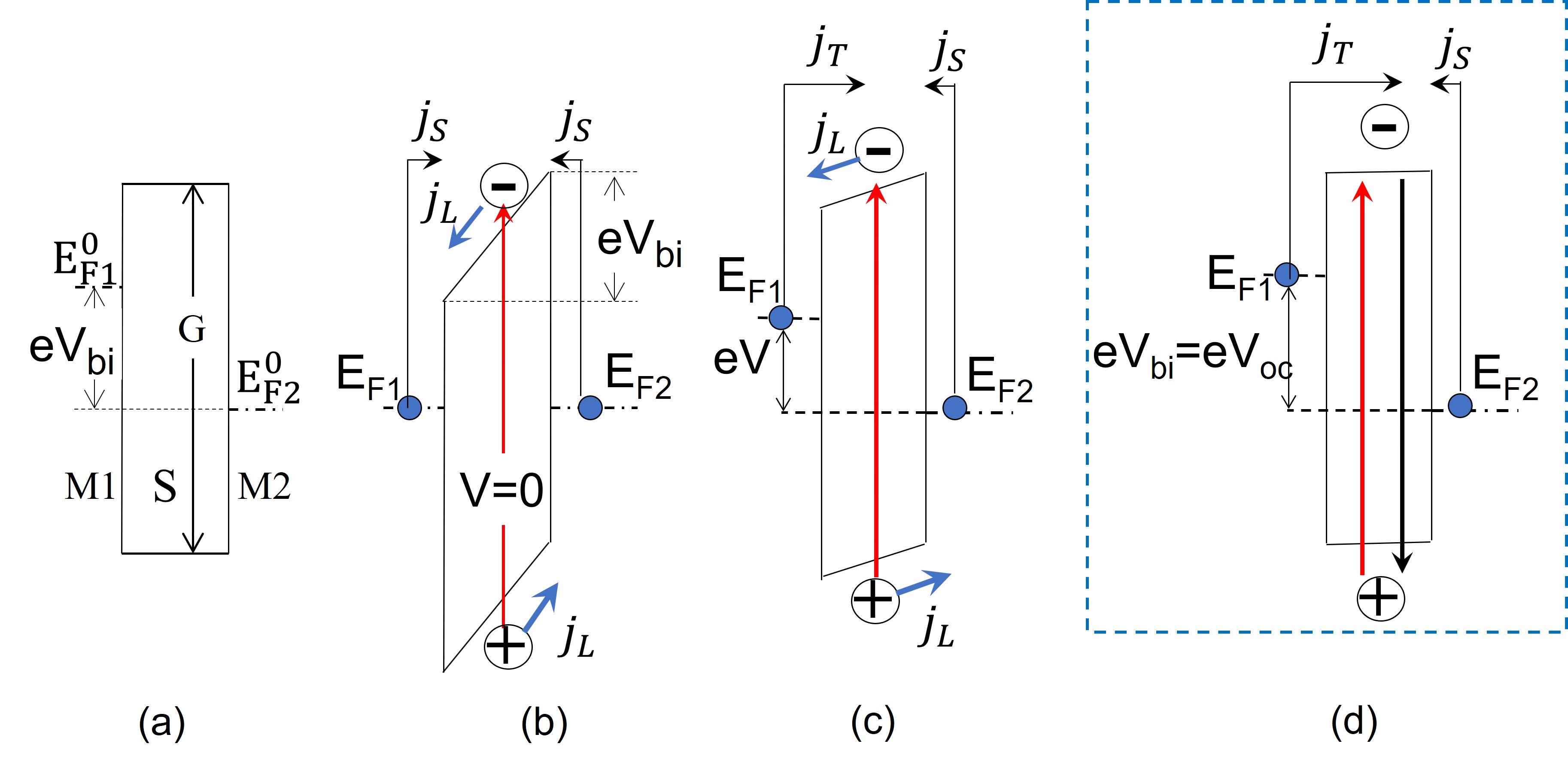
An ultimately simplified PV model in Fig. 4 accounts for the built-in uniform electric field between two metal electrodes. The electrodes work function differential results in electric charge redistribution and its corresponding built-in electric field.
Our model incorporates several simplifications:
(i) The layer is thin enough, so that the built-in field is almost uniform.
(ii) A strong enough bias when the diffusion component of current density can be neglected compared to that of drift, i. e. , where is the carrier concentration, is the velocity, is the mobility, and has its standard meaning.
(iii) The mobilities and concentrations are about the same for electrons and holes.
(iv) There is no tunneling through the layer.
(v) The photogeneration is spatially uniform.
Relaxing the above simplifications will not significantly change our conclusions below. However, the following one is of principle importance:
(vi) We assume zero recombination rate. The corresponding criterion is derived below.
For the case of suppressed recombination, the photocurrent (Fig. 4) is voltage independent, corresponding to the condition that all photogenerated carriers are collected. (The possibility of voltage dependent photocurrent [40, 41] would assume some recombination.) We note that in the approximation , the charge carrier concentration will change with electric field to maintain constant where is the carrier generation rate per area.
In the standard current voltage characteristic,
| (2) |
is the saturation current. The open circuit regime corresponds to the balance of thermal and photo currents, [3, 4, 5, 6, 7] where . The physics behind such a balance is not the same as that of sometime assumed scenario of ‘total recombination’ between photogenerated electrons and holes under the condition of flat bands [Fig. 4 (d)] corresponding to zero electric field (M.J.Heben, private communication, November 03, 2022).
The balance along with Eq. (2), yields the equation for open circuit voltage,
| (3) |
showing how is generally different from the built-in voltage depicted in Figs. 4 (a), (b). We note for comparison that the above mentioned model of zero built-in field [Fig. 4 (d)] would nullify photocurrent at , while leaving significant quasi-Fermi levels differential and its related forward current intact (we recall that the current is proportional to the gradient of quasi-Fermi levels; see e. g. Ref. [37]). Therefore, the open circuit condition is not directly related to . With that in mind, the very definition of voltage deficit in Eq. (1) as with appears questionable.
Note that using the gap dependent saturation current
| (4) |
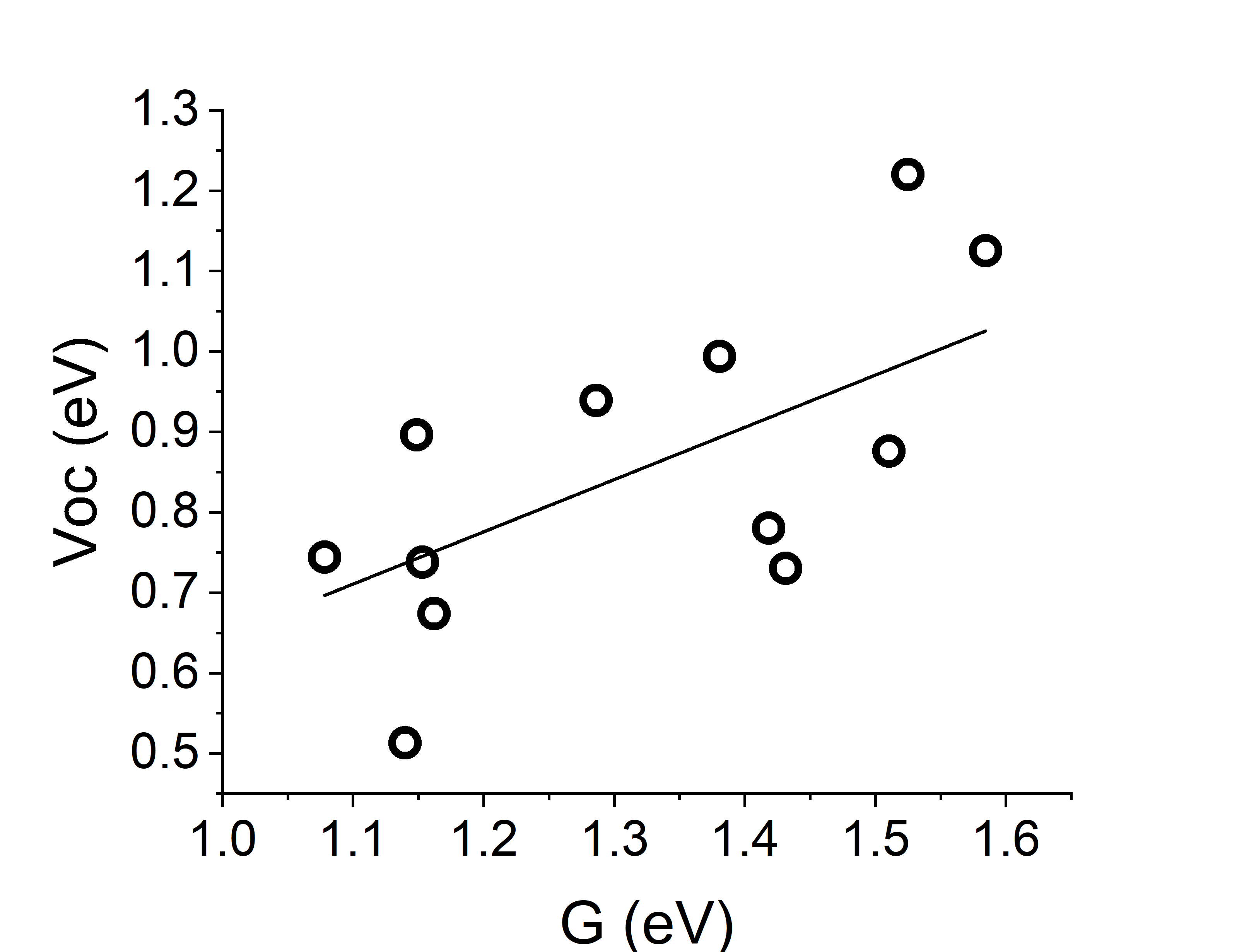
where is a material parameter, [38] Eq. (3) predicts a linear relation between and ,
| (5) |
Such a linear trend, while somewhat present in Fig. 3, is statistically weak, with the correlation coefficient of reflecting strong data dispersion.
We now compare the SRH related deterioration in electric current to that in voltage. The recombination can be described phenomenologically by modifying the carrier generation rate, where is the number of electron-hole pairs recombining per area per time. The recombination will thus decrease the photocurrent by . For relatively small Eq. (3) predicts voltage degradation . Therefore, the relative degradations in current and voltage are of the same order of magnitude,
| (6) |
i. e. SHR processes affect the current and voltage to approximately the same extent. Since in best devices the current is only slightly affected by recombination, so must be the voltage. We conclude again that SHR recombination may not be a significant factor in PV performance.
For verification, we conducted SCAPS based numerical modeling for CdTe, CIGS and simple p-n systems, which together with the published perovskite results in Table 2 confirm the same order of magnitude relative changes in current and voltage due to SHR recombination. Fig. 5 illustrates our approach to estimate the effect of recombination defect centers on CdTe based PV: starting with the ‘standard’ model, we eliminated the recombination centers first from the semiconductor components, then from the TCO as well; we used a similar approach for CIGS and simple p-n junction models. For perovskites we used the results of published simulations for PV parameters vs. defect concentrations from two independent works. We would like to emphasize here that the role of those results is to show that relative effects on current and voltage are similar (rather than quantitatively predicting those effects). In particular, if the recombination effect on current is empirically found insufficient, one should expect the same for voltage.
| Loss | CdTe | CIGS | simple p-n | Perovs1 | Perovs2 |
|---|---|---|---|---|---|
| 9.5 | 2.5 | 16.9 | 5.3 | 20 | |
| 6.6 | 5.5 | 7.8 | 11.7 | 20.5 |
IV Criterion of suppressed recombination
When comparing the recombination time to the drift time , a subtlety is that we do not immediately know the field strength . Both and velocity can be affected by the redistribution of photogenerated carriers. Here we consider the possibility of such a redistribution effect.
Sketched in Fig. 6, are the photogenerated carriers moving towards the opposite electrodes and forming two oppositely charged layers of thicknesses each. These layers create the polarization electric field opposing the original built-in field . The total electric field is related to the electric potential difference between the electrodes. Here we have introduced the photovoltage,
| (7) |
with a heuristically defined parameter .
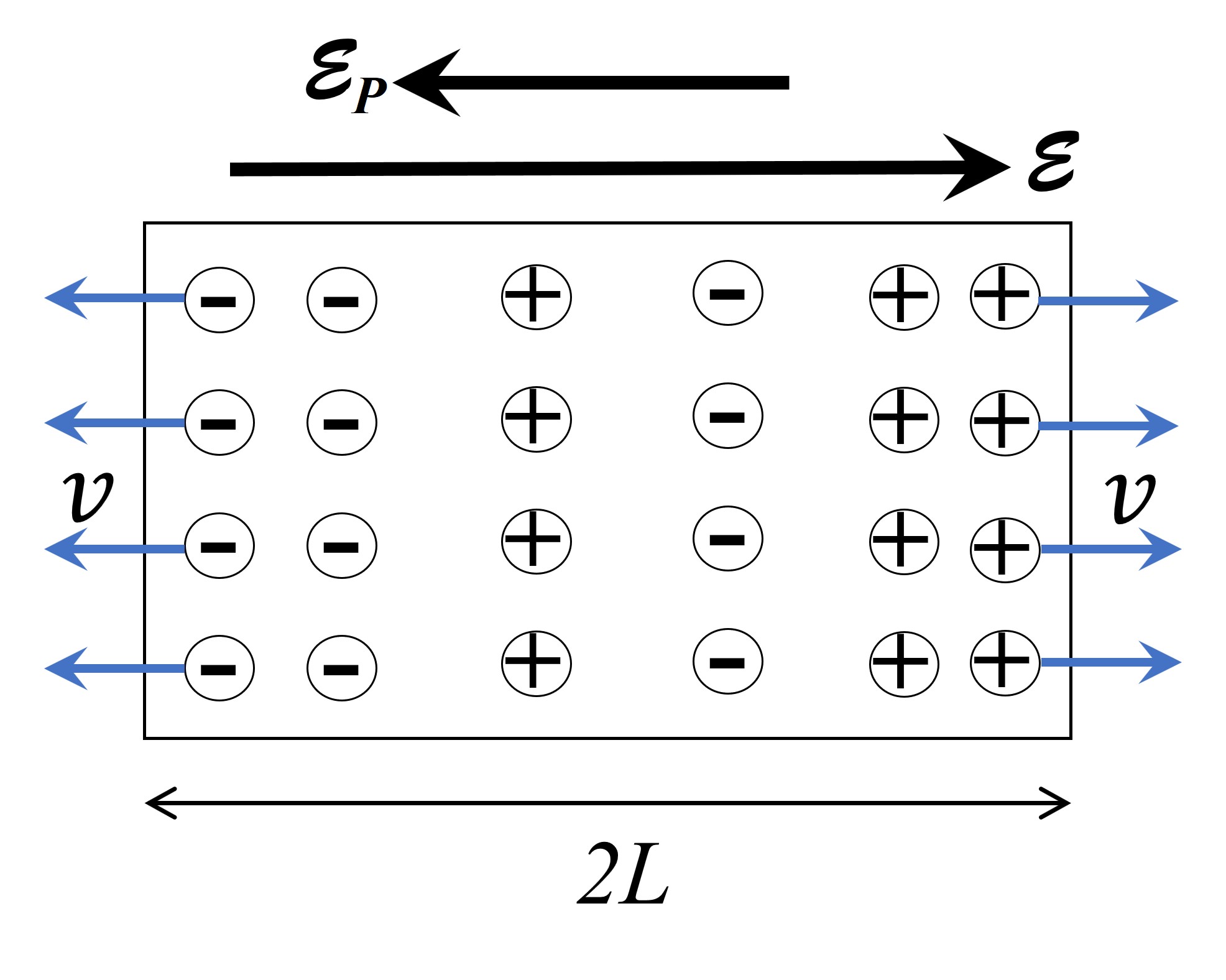
The absolute value of charge density per area is approximated as
| (8) |
Here, is the concentration of photogenerated carriers, is the generation rate (per area per time),
| (9) |
is the characteristic drift time accounting for the polarization effect.
The polarization field becomes,
| (10) |
(in Gaussian units) where is the dielectric permittivity and is the polarization surface charge density. Combining (8) and (10) yields a quadratic equation,
| (11) |
with
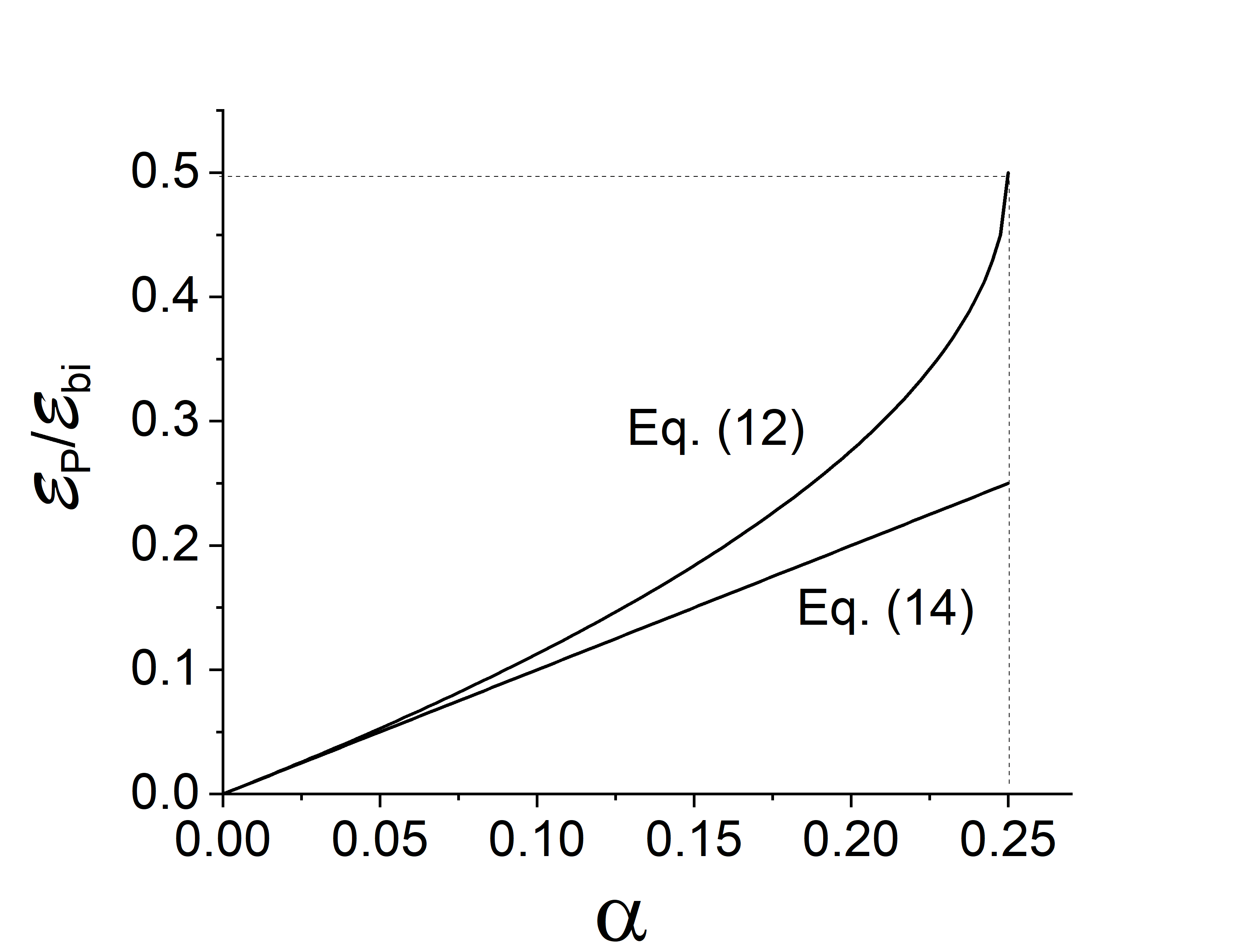
| (12) |
It is natural to call extraction delay parameter; its small values correspond to a favorable case of promptly extracted charge carriers.
To evaluate , we use with Eq.(12) a set of realistic parameters, , V,[46, 47] m, cm2V-1s-1, which yields , i. e. V. Small values of enable one to drop in Eq. (9), which reduces it to the intuitive estimate .
As follows from Eq. (11) and illustrated in Fig. 7, the photovoltage is limited to when . The upper bound reflects a maximum in polarization rate . For small , Eq. (11) yields,
| (13) |
heuristically assumed in Eq. (7). Also, our analysis predicts voltage independent photocurrent (the coefficient of 2 accounts for electrons and holes), consistent with the standard approach mentioned after Eq. (2).
On the other hand, for carrier mobilities several orders of magnitude lower, such as in polymer PV, [49, 48] the parameter can greatly exceed unity. For such low mobility structures, the drift time in Eq. (9) becomes long enough to allow the dominant recombination; hence, the suppressed recombination concept does not apply. Accordingly, there is no reason to expect in polymer PV, which conclusion is in agreement with empirical observations. [37, 50]
In fact, the latter ’recombination sensitive’ scenario can be analyzed similarly by replacing the drift time of Eq. (9) with the composite defined by,
| (14) |
including the recombination time . As a result, Eq. (11) changes to the form,
| (15) |
where is still defined by Eq. (12). Along with , there is now another parameter describing the relative significance of recombination,
| (16) |
We observe that the suppressed recombination criterion remains as suggested (), and large values of are allowed when recombination matters, i. e. . While it is straightforward to describe all possible cases of and , here we limit ourselves by concluding that the case of suppressed recombination and efficient PV corresponds to the limit .
V for suppressed recombination
Recombination out of the picture, very few possibilities remain to understand data. As a general feature, these data in Fig. 3 show (i) very significant dispersion of s, all well below the suspected ultimate values of , and (ii) almost no correlation with . A few possibilities underlying such a behavior and unrelated to SRH processes can be pointed out.
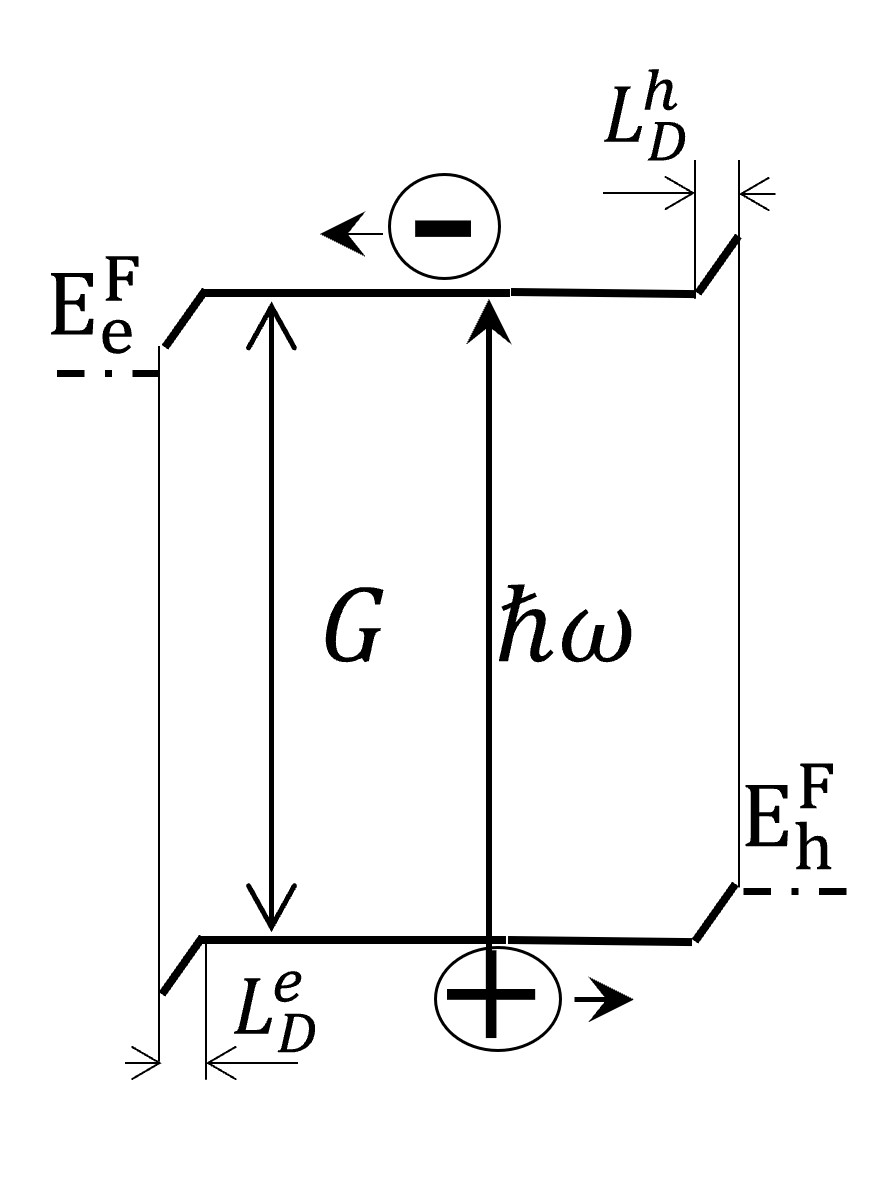
1. The electrostatic effect. The desired zero voltage deficit assumes the difference between the electron and hole quasi-Fermi levels close to the corresponding conducting () and valence () band edges and ,
| (17) |
as illustrated in Fig.8. Should the latter be the case, the concentrations of free charge carriers would become comparable to the effective state density, , where are the effective masses of electrons and holes. At room temperature K, one gets cm-3. The high concentrations of charge carriers provide strong electrostatic screening, suppressing the electric field. Therefore, the photo-generated charge carriers will have to move by diffusion instead of drift, which significantly increases their travel times, promoting recombination and degrading PV efficiency.
More quantitatively, the Debye screening lengths for electrons and holes are where is the dielectric permittivity and is the corresponding charge carrier concentrations. Using cm-3 and one gets nm, much thinner than the typical PV thickness m. The electric field is not suppressed when . With Eq. (17) in mind, the latter inequality yields,
| (18) |
Here, the numerical coefficient of 10 is obtained assuming the typical numerical values of parameters involved.
The criterion in Eq. (18) introduces the ‘ultimate’ voltage deficit [13] controlled by the electrostatic screening. It is consistent with the collection of data in Fig. 2 and 3 where none of the measured is closer to than eV. Note that such ‘ultimate’ voltage deficit does not depend on SRH recombination. While of the same order of magnitude for all conceivable semiconductors, it allows some moderate variations between them due to effective masses and working temperatures .
The above estimate of ultimate voltage deficit can be affected by considering electrostatic screening by localized states [39, 7], e. g. band tail states. We do not expect the corresponding revision to be very significant because the concentrations of tail states are typically comparable to . Yet such screening modification can make the ultimatet deficit more sensitive to material structure.
2.Meyer-Neldel (MN) rule observed in a great variety of semiconductor structures. It states that the probabilities of thermally activated processes include non-thermal exponentials in the form,
| (19) |
where is a fictitious system-sensitive temperature often in the interval of K; in some cases, negative of similar absolute values are reported. [52, 53, 54, 55, 56, 57, 58, 59, 60, 61] The physics behind MN rule remains disputable with two popular hypothesis that (a) the entropy contribution to the system free energy is proportional to (‘compensation rule’) because of the exponentially large number of combinations of small energy () excitations, for example, phonons, involved, or (b) the activation barrier energies are random. Setting aside the question of its origin, we note here that the MN rule is not related to any type of electron-hole annihilation and thus is consistent with the concept of suppressed recombination.
Taking the MN rule into account Eqs. (1) and (5) combine to yield,
| (20) |
which is qualitatively consistent with the above mentioned observations that ’s are considerably lower than ’s and rather weekly correlated witg ’s (since is independent of ). Note that in Eq. (20) links the MN rule to the diode ideality factor correctly predicting the typically observed .
While interpreting as an inherent material parameter, the result in Eq. (20) leaves the leakage current potentially attainable to technology. Furthermore, variations in can explain variations in open circuit voltage between nominally identical devices, observed more often than reported.
2. Leakiness of ohmic or non-ohmic nature not affecting the photocurrent, yet noticeably lowering can be due to microelements known as week diodes. [7, 62] Phenomenologically, the effect can be attributed to the local increase in the saturation current determining through Eq. (5).
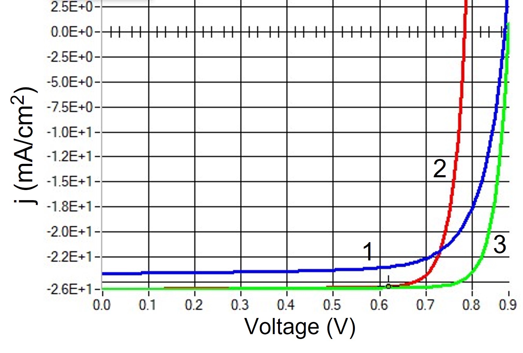
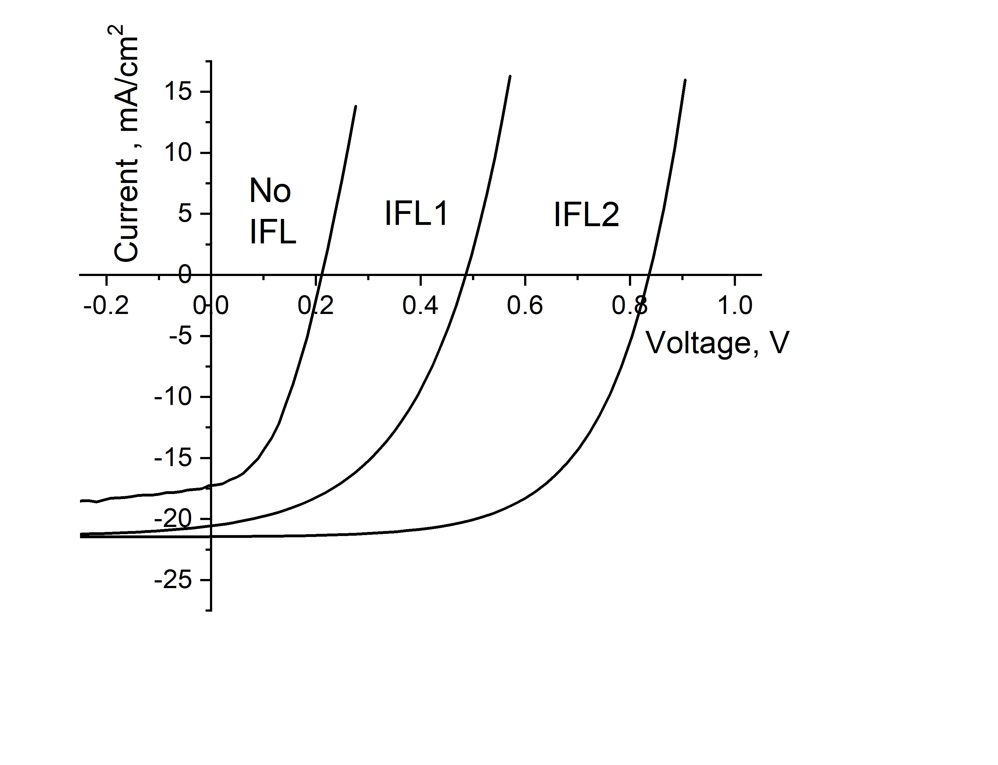
At a more microscopic level, the system is represented with a set of microdiodes possessing random local open circuit voltages (and approximately the same photocurrents), which are connected in parallel through a resistive electrode. The microdiode lateral dimensions are on a micron scale, m. Those possessing low s (weak diodes) are responsible for the macroscopic voltage deficit. The weak diodes are often related to interfacial properties. One illustration is presented in Fig. 9 based on the previously published data. [63].
A variety of microscopic mechanisms [7] can be responsible for the weak diode behavior, mostly implying leakage due to percolation in nonuniform films, such as hopping conduction through the localized states, possibly including the Urbach absorption related tail states. All of the weak diode models, perhaps even different between different materials, are reducible to the local spots of anomalously high suturation current density and that translates to low microscopic characterizing such spots. The presence of leaking spots was first observed decades ago in connection with the thermionic emission [64, 65] understood then in terms of the patch model accounting for lateral variations in metal work functions. Later, the concept of lateral variations was recognized for thin amorphous films [66] and other disordered systems [67, 68] and for thin film PV. [7, 62] It was demonstrated recently that for the case of thin films, the leaking pathways are almost rectilinear.[69]
For the open circuit regime, the condition of zero total current leads to the macroscopic (average) open circuit voltage
| (21) |
where the angular brackets stand for averaging over random microscopic . Eq. (21) explicitly shows how anomalously low (weak diode) entities have exponentially strong effect on the observed . Physically blocking such weak spots with interfacial layers will increase . This is illustrated in Fig. 9 where the existing weak diode spot is blocked by applying this or other interfacial layer (IFL).
Averaging in Eq. (21) becomes rather nontrivial [7, 62] when multiple comparably weak diodes act simultaneously within the same electrically connected domain of size
| (22) |
where is the electrode sheet resistance. All subtleties [7, 62] aside, the approximate result for the weak diode caused voltage deficit is given by
| (23) |
where is the characteristic diameter of a weak diode. The ratio can be as large as corresponding to of several tenths of one Volt in Eq. (23). Similar to the MN related , Eq. (23) explains the nature of and the data spread for materials possessing the same . Furthermore, variations in microscopic morphology can explain the often observed dispersion in open circuit voltages between nominally identical devices.
Under light, the weak diode entrances in the film interface form local spots of different electric potential, which drive lateral electric currents playing the role of current sinks. On the other hand, they can attract mobile ionic particles capable of neutralizing such spots with proper IFL. In particular, electrolytes or other passivation agents can mitigate the weak diode effects [17, 20, 22, 70]. Furthermore, if not treated, the weak diode effects can aggravate due to the positive feedback of persistent flow of localized leakage current degrading the cell performance. Therefore, passivation treatments can improve the device stability as well.
The weak diode related voltage deficit can be experimentally identified by various mappings [7, 62], by size effects leading to stronger variations among smaller size devices, and by the light intensity dependent measurements when low light conditions increase and make voltages more dispersed. [7, 62]
The above three sources of voltage deficit are all unrelated to SRH recombination, and yet they can explain the observed significant s, the existence of ‘ultimate’ V and s dispersion between devices possessing almost the same optical gaps. To avoid any misunderstanding we note that if predicted by Eqs. (20) or Eq. (23) exceeds that of Eq. (18), the latter should not be taken into account (in particular, no need to add it).
A number of uncertainties (such as the electrostatic screening by tail states, the microscopic nature of weak diodes) and unknowns (e. g., the nature of Meyer-Neldel effect) make the comprehensive understanding of suppressed recombination PV to be work in progress.
VI Conclusions
In summary, we have demonstrated the following:
-
1.
The known definition of voltage deficit [Eq. (1)] may lack sufficient empirical and theoretical grounds as a relevant voltage parameter.
-
2.
There exist the conditions of suppressed recombination and efficient carrier extraction, under which SRH recombination processes are insignificant. These conditions hold well for at least best performing thin film PV.
-
3.
There are physical factors (electrostatic screening, MN effect, and leakage) not related to SRH recombination that can significantly affect the observed PV voltage.
-
4.
Some uncertainties and unknowns remain calling upon future work towards understanding the limitations of suppressed recombination devices.
The suppressed-recombination physics presented here may not be in synergy with a culture of recombination dominated PV. [71] The well known historical circumstances underlying the latter can explain its overwhelming acceptance: (a) the first semiconductor devices were relatively thick thus giving enough time for the electrons and holes to recombine before they reach the electrodes; (b) the material quality of the first semiconductors was rather poor, with lots of imperfections promoting recombination. Hence, the SRH theory of recombination explaining the observations became a significant part of semiconductor physics.
The circumstances changed since: (a) semiconductor films of modernity are thin, down to sub-micron scales where electrons and holes may have a good chance to get extracted before they recombine; (b) the modern materials are cleaner, with fewer imperfections, so the SRH recombination may be not that strongly promoted (even in polycrystalline films structural imperfections are pushed away from the grains during crystallization; they end up at grain boundaries where their role may turn beneficial due to electric charging and coulomb repulsion forming recombination barriers [7] ). Therefore, we call for a careful differentiation between the qualities of sufficient vs necessary for the paradigm of recombination driven PV. From the practical perspectives, adopting the concept of suppressed recombination will shift the research efforts from defect chemistry to interfacial treatments and more fundamental issues such as screening and Meyer - Neldel rule.
Finally, our results here are applicable to other devices call for other developments towards suppressed recombination devices, such as thin-film semiconductor photo-detectors or light-emitting diodes. We point at our recent successful attempt to understand X-ray perovskite detectors based on suppressed recombination paradigm. [13]
References
- [1] NREL. Transforming Energy, Best Research-Cell Efficiency Chart. Available at https://www.nrel.gov/pv/cell-efficiency.html (accessed 2022-09-17).
- [2] M. A. Green, E. D. Dunlop, J. Hohl-Ebinger, M. Youshita, N. Kopidakis, X. Hao, Solar Cell Efficiency Tables (Version 59) Prog Photovolt Res Appl, 30 3-15 (2022)
- [3] A. L. Fahrenbrugh and R. H. Bube, Fundamentals of Solar Cells, Academic Press 1983.
- [4] Handbook of Photovoltaic Science and Technology, Edited by A. Lique and S. Heggedus, Wiley 2002.
- [5] J. Nelson, The Physics of Solar Cells, Imperial College 1983.
- [6] P. Wurfel, Physics of Solar Cells, Wiley-VCH 2005.
- [7] Victor Karpov and Diana Shvydka, Physics of Thin Film Photovoltaics, Wiley 2021.
- [8] W. Shockley and W. T. Read, Statistics of the recombinations of holes and electrons, Phys. Rev., 87 (1952), pp. 835–842
- [9] R. N. Hall, Electron-hole recombination in Germanium, Phys. Rev., 87 (1952), p. 387
- [10] C-T Sah, R. N. Noice, and W. Shocley, Carrier Generation and Recombination in P-N Junctions and P-N Junction Characteristics, PROCEEDINGS OF THE IRE, 1228 (1957).
- [11] W. Shockley and H. J. Queisser, Detailed Balance Limit of Efficiency of p-n Junction Solar Cells, J. Appl. Phys. 32, 510 (1961)
- [12] D. Bartesaghi, I. Perez, J. Kniepert, S. Roland, M. Turbiez, D. Neher, L. J. A. Koster, Competition between recombination and extraction of free charges determines the fill factor of organic solar cells, Nature Communications, 6, 7083 (2015); DOI: 10.1038/ncomms8083
- [13] Al. L. Efros and V. G. Karpov, Electric Power and Current Collection in Semiconductor Devices with Suppressed Electron-Hole Recombination, ACS Energy Lett. 7, 3557-3563 (2022).
- [14] J. Chantana, Yu Kawano, T.Nishimura, A. Mavlonov, T. Minemoto, Impact of Urbach energy on open-circuit voltage deficit of thin-film solar cells, Solar Energy Materials and Solar Cells 210, 110502 (2020)
- [15] C-H. M. Chuang, A. Maurano, R. E. Brandt, G. W. Hwang, J. Jean, T. Buonassisi, V. Bulović,and M. G. Bawendi, Open-Circuit Voltage Deficit, Radiative Sub-Bandgap States, and Prospects in Quantum Dot Solar Cells, Nano Lett. bf 15, 3286–3294 (2015)
- [16] S. Kim, K. M. Kim, H. Tampo, H. Shibata, and S. Niki, Improvement of voltage deficit of Ge-incorporated kesterite solar cell with 12.3% conversion efficiency, Appl. Phys. Express 9, 102301 (2016) DOI 10.7567/APEX.9.102301
- [17] X. Yi, Y. Mao, L. Zhang, J. Zhuang, Y. Zhang, N. Chen, T. Lin, Y. Wei, F. Wang, J. Wang, C. Li, Reducing Open-Circuit Voltage Deficit in Perovskite Solar Cells via Surface Passivation with Phenylhydroxylammonium Halide Salts, Small methods, 2000441 (2020) DOI: https://doi.org/10.1002/smtd.202000441
- [18] J-S. Park, S. Kim, S. N. Hood, and A. Walsh, Open-circuit voltage deficit in Cu2ZnSnS4 solar cells by interface bandgap narrowing, Appl. Phys. Lett. 113, 212103 (2018); https://doi.org/10.1063/1.5063793
- [19] S. Shukla, D. Adeleye , M. Sood , F. Ehre, A. Lomuscio , T.P. Weiss, D. Siopa, M. Melchiorre , and S. Siebentritt, Carrier recombination mechanism and photovoltage deficit in 1.7-eV band gap near-stoichiometric Cu(In,Ga)S2, Phys. Rev. Mat. 5, 055403 (2021)
- [20] C. Wang, X.Wang, Z. He, B.Zhou, D.Qu, Y. Wang, H.Hu, Q. Hu, Y.Tu, Minimizing voltage deficit in Methylammonium-Free perovskite solar cells via surface reconstruction, Chem. Eng. J., 444 136622 (2022).
- [21] B. Subedi, C. Li, C. Chen, D. Liu, M. M. Junda, Z. Song, Y. Yan, and N. J. Podraza, Urbach Energy and Open-Circuit Voltage Deficit for Mixed Anion–Cation Perovskite Solar Cells, Appl. Mater. Interfaces, 14 7796–7804 (2022), DOI: https://doi.org/10.1021/acsami.1c19122
- [22] M. Sood, A. Urbaniak, CK Boumenou, T.P. Weiss, H. Elanzeery, F. Babbe, F. Werner, M. Melchiorre, S. Siebentritt, Near surface defects: Cause of deficit between internal and external open-circuit voltage in solar cells, Progress in Photovoltaics,30, 263 (2022); DOI10.1002/pip.3483
- [23] M. Koopmans, L.J.A Koster, Voltage Deficit in Wide Bandgap Perovskite Solar Cells: The Role of Traps, Band Energies, and Effective Density of States, Solar RRL, Article number 2200560, (2022); DOI10.1002/solr.202200560
- [24] C. Chen, J. Tang, Open-Circuit Voltage Loss of Antimony Chalcogenide Solar Cells: Status, Origin, and Possible Solutions, ACS Energy Letters, 5, 2294-2304 (2020); DOI10.1021/acsenergylett.0c00940
- [25] D. Kuciauskas, SM Li, J. Moseley, D. Albin, C. Lee, AL Onno, ZC Holman, Voltage Loss Comparison in CdSe/CdTe Solar Cells and Polycrystalline CdSeTe Heterostructures, IEEE Journal of Photovoltaic, 12, (2022); DOI: 10.1109/JPHOTOV.2021.3117914
- [26] M. Daboczi, I. Hamilton, S. Xu, J. Luke, S. Limbu, J. Lee, MA McLachlan,K. Lee, J. R. Durrant, I. D. Baikie, and J-S Kim, Origin of Open-Circuit Voltage Losses in Perovskite Solar Cells Investigated by Surface Photovoltage Measurement, ACS Appl Mater Interfaces 11, 46808 (2019); DOI: 10.1021/acsami.9b16394
- [27] B. Hallam, D. Chen, J.Shi,R. Einhaus, ZC Holman, S. Wenham, Pre-Fabrication Gettering and Hydrogenation Treatments for Silicon Heterojunction Solar Cells: A Possible Path to ¿ 700 mV Open-Circuit Voltages Using Low-Lifetime Commercial-Grade p-Type Czochralski Silicon, Solar RRL, 2, Article Number1700221; DOI:10.1002/solr.201700221 (2018).
-
[28]
data from the ossila website
https://www.ossila.com/en-kr/pages/perovskites-and-perovskite-solar-cells-an-introduction. - [29] J. L. Gray, The physics of Solar Cells, in Handbook of Photovoltaic Science and Engineering, p. 61, Edited by A. Lique and S. Heggedus, Wiley (2002).
- [30] A. G. Milns, Deep impurities in semiconductors, Wiley Interscience (1973).
- [31] D. K. Schroder, Carrier Lifetimes in Silicon, IEEE Trans. Electron Devices, 44, 160 (1997).
- [32] S. Parola, et al, Study of photoluminescence decay by time-correlated single photon counting for the determination of the minority-carrier lifetime in silicon, 4th International Conference on Silicon Photovoltaics, SiliconPV 2014, Energy Procedia 55, 121 (2014).
- [33] S. Khatavkar et al, Measurement of Relaxation Time of Excess Carriers in Siand CIGS Solar Cells by Modulated Electroluminescence, Technique, Phys. Stat. Solidi. A, 215, 1700267 (2018).
- [34] V. N. Abakumov, V. I. Perel, I. N. Yassievich, Nonradiative Recombination in Semiconductors (Modern Problems in Condensed Matter Sciences), North-Holland (1991).
- [35] P.T. Landsberg, Recombination in Semiconductors, Cambridge University Press (1991).
- [36] S. Rein, Lifetime Spectroscopy: A Method of Defect Characterization in Silicon for Photovoltaic Applications, Springer Series in Materials Science, Springer 2005.
- [37] L. J. Koster, V. D. Mihailetchi, R. Ramaker, and P. W. Blom, Light intensity dependence of open-circuit voltage of polymer:fullerene solar cells, Appl. Phys. Lett. 86, 123509 (2005); doi: 10.1063/1.1889240
- [38] T. J. Coutts, J. S. Ward, D. L. Young, K. A. Emery, T. A. Gessert, and R. Noufi, Critical Issues in the Design of Polycrystalline, Thin-film Tandem Solar Cells, Prog. Photovolt: Res. Appl. 11, 359–375 (2003); (DOI: 10.1002/pip.491).
- [39] N. F. Mott and E. A. Davis, Electronic Processes in Non-Crystalline Materials, Second Edition, Oxford University Press (1979)
- [40] Hegedus, S.; Desai, D.; Thompson, C. Voltage dependent photocurrent collection in CdTe/CdS solar cells. Prog. Photovolt. Res. Appl. 2007, 15, 587–602
- [41] C. X. Zhao, K. K. Chin, A Theoretical Model for Voltage-Dependent Photocurrent Collection in CdTe Solar Cells, Energies, 14, 1615 (2021); https://doi.org/10.3390/en14061615
- [42] M. Gloeckler, A.L. Fahrenbruch, J.R. Sites, Numerical modeling of CIGS and CdTe solar cells: setting the baseline, 3rd World Conference onPhotovoltaic Energy Conversion, Osaka, Japan IEEE (2003)
- [43] SCAPS 3.3.02 ELIS-UGent: Version scaps3302.exe, dated 28-08-2015. M. Burgelman, J. Verschraegen, B. Minnaert, J. Marlein, Numerical simulation of thin film solar cells : practical exercises with SCAPS, NUMOS (International Workshop on Numerical Modelling of Thin Film Solar Cells), 28-30 March, 2007, Ghent, Belgium, Academia Press , 2007, p. 357-366.
- [44] Du, H. J., Wang, W. C., Zhu, J. Z. Device simulation of lead-free CH3NH3SnI3 perovskite solar cells with high efficiency. Chin. Phys. B 25, 108802–188809 (2016).
- [45] S. S. Hussain , S. Riaz, G. A. Nowsherwan, K. Jahangir, A. Raza, M. J. Iqbal, I. Sadiq, S. M. Hussain,and S. Naseem, Numerical Modeling and Optimization of Lead-Free Hybrid Double Perovskite Solar Cell by Using SCAPS-1D, Journal of Renewable Energy Volume 2021, Article ID 6668687, https://doi.org/10.1155/2021/6668687
- [46] S.M.Sze, Physics of Semiconductor Devices, Second Edition, Wiley 1981.
- [47] Wikipedia article ‘Work function’, https://en.wikipedia.org/wiki/Work_function (accessed 2022-12-11)
- [48] Y. Li and Y. Zou, Conjugated Polymer Photovoltaic Materials with Broad Absorption Band and High Charge Carrier Mobility, Adv. Mater. 20, 2952 (2008); DOI: 10.1002/adma.200800606
- [49] B. Ebenhoch, S. A.J. Thomson, K. Genevicius, G. Juska, I. D.W. Samuel, Charge carrier mobility of the organic photovoltaic materials PTB7 and PC71BM and its influence on device performance, Organic Electronics, 22, (2015); DOI: https://doi.org/10.1016/j.orgel.2015.03.013.
- [50] D. Credgington and J. R. Durrant, Insights from Transient Optoelectronic Analyses on the Open-Circuit Voltage of Organic Solar Cells, J. Phys. Chem. Lett. 3, 1465 (2012); dx.doi.org/10.1021/jz300293q
- [51] M. Grundmann, The Physics of Semiconductors. An Introduction Including Nanophysics and Applications, Springer Heidelberg Dordrecht London New York 2010.
- [52] T. J. Coutts and N. M. Pearsall, Meyer–Neldel rule in solar cells, Appl. Phys. Lett. 44, 134 (1984); doi: 10.1063/1.94578
- [53] C. Goradia and V. G. Weizer, Applicability of the Meyer–Neldel rule to solar cells, Appl. Phys. Letters 45, 1298 (1984); doi: 10.1063/1.95125
- [54] F. H. Seymour, V. Kaydanov, T. R. Ohno, Study of deep electronic states in CdTe solar cells through the detection and DLTS treatment of slow transients, Conference Record of the Thirty-first IEEE Photovoltaic Specialists Conference, 2005. DOI:10.1109/PVSC.2005.1488122
- [55] K. Prasai, P. Biswas, and D. A. Drabold, Electrons and phonons in amorphous semiconductors, Semicond. Sci. Technol.31, 073002 (2016), doi:10.1088/0268-1242/31/7/07300
- [56] H. Schmidt, M. Wiebe, B. Dittes, M. Grundmann, Meyer-Neldel rule in ZnO, Appl. Phys. Lett. 91, 232110 (2007); doi: 10.1063/1.2819603
- [57] A. Yelon and B. Movaghar, R S Crandall, Multi-excitation entropy: its role in thermodynamics and kinetics, Rep. Prog. Phys. 69, 1145 (2006); doi:10.1088/0034-4885/69/4/R04
- [58] E. B. Starikov, ‘Meyer-Neldel Rule’: True History of its Development and its Intimate Connection to Classical Thermodynamics, Journal of Applied Solution Chemistry and Modeling, 3, 15 (2014); DOI: http://dx.doi.org/10.6000/1929-5030.2014.03.01.3
- [59] R. Widenhorn, M. Fitzgibbons, and E. Bodegom, The Meyer-Neldel rule for diodes in forward bias, J. Appl. Phys. 96, 7379 (2004); doi: 10.1063/1.181835
- [60] N. Takamure, X. Sun, T. Nagata, A. Ho-Baillie, N. Fukata, and D. R. McKenzie, Thermodynamic Interpretation of the Meyer-Neldel Rule Explains Temperature Dependence of Ion Diffusion in Silicate Glass, Phys. Rev. Lett., 129, 175901 (2022); DOI:https://doi.org/10.1103/PhysRevLett.129.175901
- [61] S. D. Savransky and A. Yelon, Interpretation and consequences of Meyer–Neldel rule for conductivity of phase change alloys, Phys. Status Solidi A 207, 627 (2010) / DOI 10.1002/pssa.200982663
- [62] V.G. Karpov, A.D. Compaan, Diana Shvydka, Effects of nonuniformity in thin-film photovoltaics, Appl. Phys. Lett., 80, 4256 (2002); DOI: https://doi.org/10.1063/1.1483118. Random diode arrays and mesoscale physics of large-area semiconductor devices, Phys. Rev. B 69, 045325 (2004); DOI:https://doi.org/10.1103/PhysRevB.69.045325.
- [63] Y. Roussillon, D. Giolando, Diana Shvydka, A. D. Compaan, and V. G. Karpov, Blocking thin film nonuniformities: photovoltaic self-healing, Appl.Phys.Lett. 84, 616 (2004).
- [64] J. A. Becker, Thermionic Electron Emission and Adsorption, Rev. Mod. Phys., 7, 95 (1935); DOI: https://doi.org/10.1103/RevModPhys.7.95
- [65] C. Herring, M. H. Nichols, Thermionic Emission, Rev. Mod. Phys. 21, 185 (1949); DOI:https://doi.org/10.1103/RevModPhys.21.185
- [66] M. Pollak and J. J. Hauser, Note on the Anisotropy of the Conductivity in Thin Amorphous Films, Phys. Rev. Lett. 31, 1304 (1973); DOI:https://doi.org/10.1103/PhysRevLett.31.1304.
- [67] M. E. Raikh and I. M. Ruzin, in Mesoscopic Phenomena in Solids, edited by B. L. Altshuller, P. A. Lee, and R. A. Webb, Elsevier, New York, 1991, p. 315.
- [68] S D Baranovskiiy, T Fabery, F Hensely and P Thomas, The applicability of the transport-energy concept to various disordered materials, J. Phys.: Condens. Matter 9 2699 (1997); DOI: 10.1088/0953-8984/9/13/007
- [69] M. Patmiou, V. G. Karpov, S. Gursel, B.R. Weborg, Numerical modeling of percolation conduction and Poole-Frenkel laws, J. Appl. Phys. 128, 035701 (2020);
- [70] V. G. Karpov, Y. Roussillon, D. Shvydka, A.D. Compaan, D. M. Giolando, Photovoltaic healing of non-uniformities in semiconductor devices, United States Patent, US 7.098.058 B1, Aug. 29 (2006)
- [71] M. A. Scarpulla, B. McCandless, A. B. Phillips et al, CdTe-based thin film photovoltaics: Recent advances, current challenges and future prospects, Solar Energy Materials and Solar Cells 255, 112289 (2023); DOI: https://doi.org/10.1016/j.solmat.2023.112289 .