Bismuth Phase Dependent Growth of Superconducting NiBi3 Nanorods
Abstract
We report a study on the growth of NiBi3 nanowires and nanorods during the preparation of superconducting NiBi3 films by co-evaporation of Ni and Bi. We find that NiBi3 films grown via co-evaporation of Ni and Bi metals achieve higher transition temperatures (4.4 K) compared even to the single crystal NiBi3. However, in certain parameter space, the film surfaces were spattered with nanoscale features, such as nanowires and nanorods. Ambient temperature deposition resulted in poly-crystalline NiBi3 nanorods which were controllable with the evaporation rate of Bi. Deposition at elevated temperatures promoted the emergence of long single crystalline NiBi3 nanorods. High resolution transmission electron microscopy measurements confirmed the crystalline behaviour of the nanorods. We believe that NiBi3 nanowires form in a process analogous to the well known vapor-liquid-solid process, as we observe an amorphous Bi cap on the nanorods. From glancing angle X-ray diffraction measurements we identify that the presence of trigonal Bi with hexagonal primitive cell in the film promotes the nucleation of nanorods. Electrical transport on a single NiBi3 nanowire shows a superconducting transition of 4.3K.
keywords:
NiBi3; Nanorod growth; HRTEMCenter for Interdisciplinary Sciences (CIS), NISER Bhubaneswar, Jatni-752050, Odisha, India. \alsoaffiliationCenter for Interdisciplinary Sciences (CIS), NISER Bhubaneswar, Jatni-752050, Odisha, India.
![[Uncaptioned image]](/html/2306.12034/assets/TOC.jpg)
1 Introduction
Numerous intermetallic compounds have been discovered possessing outstanding properties usually not found in common metals and alloys1. One such interesting class of intermetallic compounds, consisting of strong ferromagnetic elements such as Ni and Co, also exhibit superconductivity2, 3, 4, 5, 6. It is well known that ferromagnetic order strongly competes with superconducting order. Even atomically dispersed ferromagnetic impurities are known to drastically suppress the superconducting order parameter in superconductors7. Therefore, the existence of two macroscopic quantum orders in one single system is fundamentally a very appealing situation, apart from the technological potentials. For the same reason, the discovery of Fe based high temperature superconductors8, 9 sparked a lot of excitement. In this context the bimetallic Nickel-Bismuth alloy also exhibits two stable phases, NiBi3 and NiBi which are superconducting with nearly equal Tc of 4.2 K and 4.1 K10, 11, 12, 13, 14. Although there have been conflicting reports on the co-existent superconductivity and magnetism11, 10, 12, 13, 14, 15, 16 in NiBi3 system, the very fact that the superconductor is based on a strongly ferromagnetic element, is interesting in itself. Coexistence of superconductivity and ferromagnetism in Bi-Ni system was first reported by LeClair et al. in a bilayer Bi/Ni system17. For certain low thickness of Ni, using spin polarized tunnelling techniques, they observed a clear superconducting gap and a spin polarization of the conduction electrons signifying ferromagnetism. Transport measurements on polycrystalline NiBi3 samples by Piñeiro et al.16 and on single crystalline NiBi3 samples by Herrmannsdörfer et al. 18 have shown that superconducting order appears well within ferromagnetically ordered state while no Ni impurities were detected in the samples. In fact, Piñeiro et al.16have shown that the ferromagnetic ordering sets in at a much higher temperature compared to the Curie temperature of Ni. There is also theoretical evidence3 supporting the coexistence of these two orders. On the other hand, Silva et al.14 have reported that ferromagnetism in the NiBi3 system appears due to the inclusion of amorphous Ni impurities. Recent high resolution surface magneto-optic Kerr effect 19 also did not observe any ferromagnetism in single crystal NiBi3 samples. Electron spin resonance experiments by Zhu et al. 13suggested that only a surface ferromagnetic fluctuation exists in NiBi3 crystals. Therefore, the coexistence of superconductivity and ferromagnetism is still an interesting debatable topic.
Several techniques have been employed for the preparation of this bimetallic superconducting NiBi3 compound in order to explore its diverse properties. For example, Sakurai et al.20 prepared polycrystalline NiBi3 by co-melting high purity Ni and Bi from 900∘ C to 1100∘ C and studied the thermoelectric, thermogalvanomagnetic properties of this system. A similar method of high temperature melting of Bi and Ni was used by Fujimori et al.11 to prepare NiBi3 polycrystals and needle crystals for finding the superconducting, normal state properties of this system.
In the thin film form, it has been found that NiBi3 compound forms at the interface of Ni and Bi prepared at room temperature 21, 22, 23, 24, 2, 25, 26, 27. The NiBi3 layer formed in this way, however, is confined only to the interface. Till now there are very few reports28 on thin films of NiBi3. It is known from earlier literature from several groups that the combination of Ni and Bi is highly diffusive in nature which is due to the lower formation energy of NiBi3 compared to individual Ni and Bi. As a result, the relative abundance of these two elements in a physical vapour deposition process and the available thermal energy at the substrate can drastically alter the microstructural evolution of the NiBi3 films formed by physical vapour deposition process. While the strongly reactive nature of the Ni and Bi elements favors the formation of NiBi3, it also leads to diverse surface texture and topographical features on the thin films in certain parameter windows, which the co-evaporation process allows to tune. Therefore, the primary motivation of this manuscript is to demonstrate this strong dependence of microstructural growth on the above mentioned parameters. We find that a higher evaporation rate of Bi, which leads to an excess of Bi impurity in the NiBi3 films, triggers polycrystalline nanowire like outgrowth on the film surface. A similar effect was observed when the co-deposition of Ni and Bi was carried out at elevated surface temperatures. In this case, however, very long crystalline nanowires of NiBi3 were found on the surface of the NiBi3 films. The growth of these crystalline nanowires was discussed in the light of the well known vapour-liquid-solid (VLS) method. We have also identified that the presence of Bi with hexagonal primitive cell promotes such anisotropic vertical growth of NiBi3 in the form of polycrystalline and single crystalline nanowires.
2 Experimental
Bismuth ingots (99.99 pure) and Nickel wires (99.999 pure) were simultaneously evaporated from thermal and e-beam ports respectively in a deposition chamber maintained at a base pressure of 110-7 mbar. A series of thin films were prepared by varying parameters such as Bi deposition rate and substrate temperature in order to understand the effect of these parameters on the microstructure of NiBi3. For the first batch of samples, the Ni deposition rate was fixed at 0.1 Å/s while the Bi deposition rate was 0.2 Å/s (named Sample A), 0.4 Å/s (named Sample B), and 0.8 Å/s (named Sample C). Another batch of co-evaporated samples was prepared by varying the substrate temperature as 150∘ C (named Sample D) and 250∘ C (named sample E) for a fixed deposition rate of Bismuth as 0.4Å/s.
A field emission scanning electron microscope (FESEM) was used to examine the surface morphology. The influence of evaporation rate of Bi and the effect of elevated substrate temperature on the phase of NiBi3 was studied using a grazing incidence X-ray diffraction (GIXRD) approach using a Cu K source with a Rigaku automated X-ray diffractometer at a grazing angle of 1.0 degree with a step size of 0.02deg. An energy-dispersive X-ray spectrometer (EDXS) attached to the FESEM column was used to perform elemental mapping on single nanorods. High resolution transmission electron microscopy (HRTEM) Jeol F200, operating at 200 keV was used to verify the crystalline structure of single NiBi3 nanorods. Low temperature resistance meausrement was performed on a single NiBi3 nanowire using cryogenic physical property measurement system (PPMS) with a minimum achievable temperature of 1.8 K.
3 Results and discussion
3.1 Effect of the evaporation rate of Bismuth
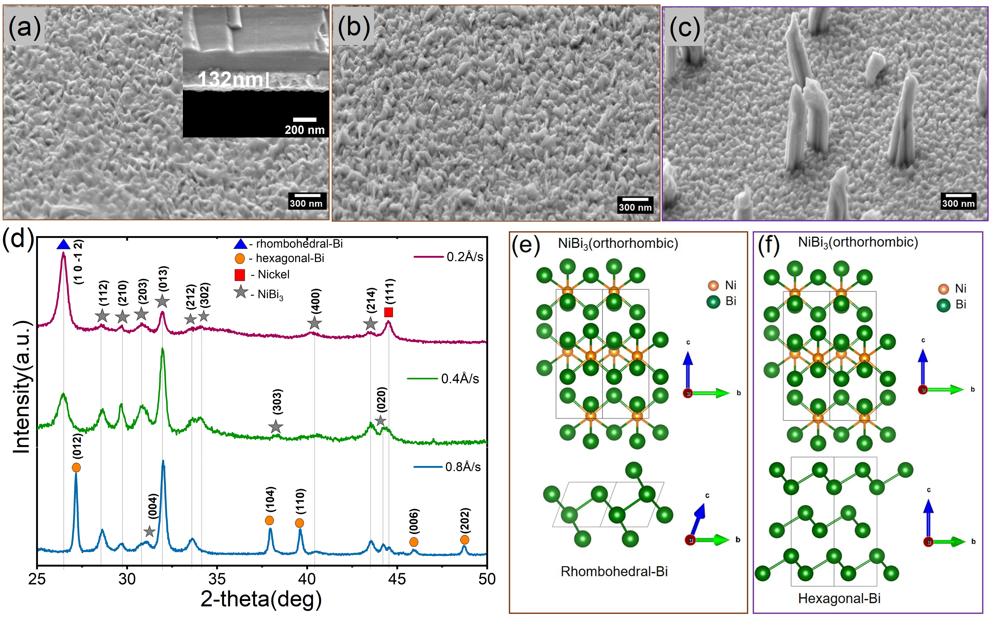
For samples A, B, and C, after attaining base vacuum in the deposition system, the evaporation rate of Ni was fixed at 0.1 Å/s in presence of a mechanical shutter in front of the substrates. Subsequently, the evaporation rate of Bi was set, prior to opening the shutter. With the increasing rate of Bi evaporation, the Ni to Bi ratio in the vapor flux decreases, leading to excess Bi in the films. Figures 1(a), (b), and (c) display the FESEM images of samples A, B, and C, respectively, captured at the same magnification and the same tilt angle of 54 degrees from the surface of the film. It is observed that the surface roughness increases slightly with an increase in the evaporation rate of bismuth which is consistent with the previously reported literature29, 30. We notice a considerable number of composite nanorod-like outgrowth with a typical height between 1 to 2 m in sample-C as shown in Fig. 1(c). Inset cross-sectional SEM image in Fig. 1(a) gives information on the thickness of the corresponding film.
The nanorod like vertical outgrowth may be reminiscent of the well known vapor-liquid-solid mechanism of nanowire growth in chemical vapour deposition31, 32. Since Bismuth has a very low melting temperature of 270 oC, the Bi vapour approaching the surface of the substrate is likely to be very mobile. Therefore, Bi on the surface may mimick the role of the liquid phase of the vapour-liquid-solid process to facilitate the growth of the nanorods.
The GIXRD plot for all three samples is shown in Fig. 1(d). Multiple peaks of orthorhombic NiBi3 system could be identified from these plots out of which (013) peak at 31.95∘ is the strongest in all the cases. However, we see an interesting change in the position of the Bi peak in the sample-C compared to the sample-A and sample-B. Bi belongs to the trigonal lattice system with space group R-3m(166). The trigonal lattice system with three-fold rotational symmetry has two sub groups with (i) Rhombohedral and (ii) Hexagonal primitive cells. From Rietveld refinement, the Bi peaks appearing in sample-A and sample-B were identified as the peaks corresponding to the rhombohedral primitive cell system, hereafter termed as ”rhombohedral-Bi”. The lattice parameters of the rhombohedral-Bi are a=b=c=4.798 Å, ===57.423∘ as per the ICSD:064703. However, in case of sample-C, the Bi peaks were identified as peaks corresponding to the hexagonal primitive cell of Bi, hereafter termed as ”hexagonal-Bi”. The corresponding lattice parameters are a=b=4.546 Å, c=11.862 Åand ==90∘, =120∘ (JCPDS file no:85-1329). Therefore, it appears that the hexagonal axis symmetery of trigonal Bi phase may be promoting the growth of NiBi3 nanorods, as these nanorods are seen only in sample-C.
We note that the orthorhombic NiBi3 has lattice parameters a=8.884 Å, b=4.15882 Å, c=11.485 Å(JCPDS file no:65-0088). Fig. 1(e) and (f) show the 2D representation of the unit cell stacking of orthorhombic NiBi3 as compared to the unit cell stacking of hexagonal-Bi and rhombohedral-Bi phases, as seen from the (100) zone axis. This 2D-representations modeling is done using VESTA program33. The illustrations in Fig. 1(e) and (f) clearly indicates that the lattice parameters of the hexagonal-Bi are closer to the lattice parameters of orthorhombic NiBi3 compared to the rhmbohedral-Bi. Therefore, the hexagonal-Bi is more likely to promote preferential growth of NiBi3 nanorods. This may be the major reason for the growth of nanorods in sample-C, where hexagonal-Bi was found. The GIXRD figure also shows that when the evaporation rate of Bi increases from 0.2 Å/s to 0.4 Å/s, the strength of all NiBi3 peaks increases, while simultaneously, the intensity of Bi peak decreases. This increase in relative intensity of NiBi3 indicates that more Bi is being used in the diffusion process to form NiBi3 compound28. The drop in the relative intensity of Ni in sample-B is also consistent with this observation. In the case of sample-C, there are other NiBi3 planes such as (1 1 2), (0 0 4), (2 1 2), (2 1 4), (0 2 0) become prominent and corresponding FWHM also decreases compared to other two samples. In addition to this, another notable finding from this GIXRD plot is the NiBi3 (0 2 0) plane close to Ni (1 1 1) starts to appear in sample-B giving rise to the broadening of the peak. The relative intensity of NiBi3 (0 2 0) increases with further increase in the evaporation rate of bismuth to 0.8Å/s.
3.2 Effect of substrate temperature
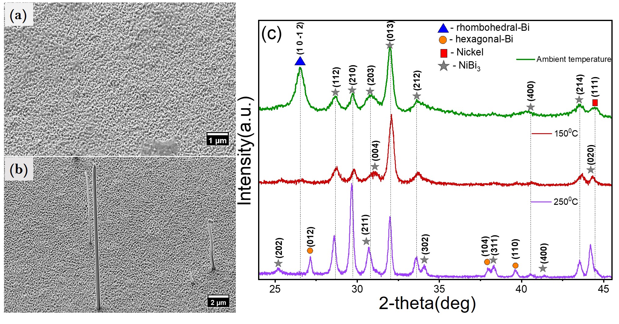
In order to further ascertain the correlation between the Bi-phase and the nanowire/nanorod growth, we have prepared another set of co-evaporated samples by varying substrate temperature to 150∘C (sample-D), 250∘C (sample-E). Fig. 2(a) and (b) represent the FESEM images of the two samples deposited at elevated substrate temperatures. Fig. 2(a) shows that although the sample surface has a significant degree of surface roughness, there are no signatures of nanorods. However, very long nanowires can be seen on the surface of sample-E, in Fig. 2(b). These nanowires appear to be quite distinct from the nanorods shown and discussed in the previous section. These nanowires are much longer and less dense than the nanorods shown in Fig. 1(c). The length of nanowires varies from 10 to 25 m with an average width of 300 nm. There are no previous reports on such longer NiBi3 nanowires prepared by the physical vapour deposition process. The effect of substrate temperature has been found to be significant for the formation of nanowires29. Since Bi has a melting point of 271.4∘C, a sample deposited around this temperature is expected to have enough thermal energy for the crystallization of NiBi3 nanowires.
Fig. 2(c) shows the GIXRD plots of samples D and E, along with the ambient temperature grown film at the same evaporation rates of Ni and Bi. In all three graphs, there are appreciable numbers of NiBi3 peaks, as well as a few bismuth peaks. There is a broad peak visible for Ni (1 1 1) plane in the ambient temperature grown sample whereas, in the other two samples, the relative intensity of nickel has decreased significantly. At the same time, the intensity of the NiBi3 (0 2 0) plane at 44.131∘ close to Ni (111) peak 44.45∘ has enhanced. The other noteworthy feature of the GIXRD pattern of sample-E, grown at temperatures close to the melting point of Bi, is the appearance of significantly more number of NiBi3 peaks. The thin film undergoes re-crystallization process by the temperature during deposition, which has been investigated by many researchers34, 35, 36, 37. It is also known that with increasing substrate temperature, the average crystallite size increases34. Consequently, it is noticed that the FWHM of NiBi3 peaks decrease significantly with increasing substrate temperature.
In addition, there is an enhancement of NiBi3 peaks with hkl planes (3 0 2), (3 1 1), and (0 2 0) corresponding to 2-theta values 34.036∘, 38.269∘, and 44.131∘ (close to the 2-theta value of Ni) which again confirms the re-crystallization process34. The GIXRD data in the Fig 2 shows that the 250∘C deposited Sample-E, which nucleated very long nanowires of NiBi3, has Hexagonal-Bi (JCPDS file no:85-1329) phase. Similar to the previous section, we notice that congruent growth of nanowires appears only in sample-E, where the underlying Bi has a hexagonal primitive cells. In the subsequent section, we focus on a detailed analysis of the two types of NiBi3 nanowires obtained in the two cases.
3.3 Characterization of NiBi3 nanowires
3.3.1 EDAX and HRTEM analysis
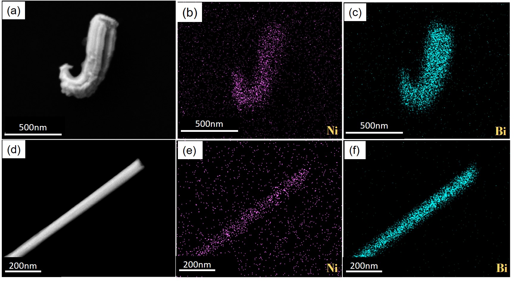
We have performed EDAX and HRTEM on the two types of nanowires after scratching them onto a carbon-coated Cu grid to confirm the elemental distribution and crystalline nature. Fig. 3 shows the FESEM image and EDAX elemental mapping of the nanorods. Fig. 3(a) is the FESEM image for the rods that appeared on Sample-C, which was grown at ambient substrate temperatures. Fig. 3(b) and (c) depict the elemental EDAX mapping of Ni and Bi in this nanorod, demonstrating the presence of both Ni and Bi throughout. Similarly, the FESEM image of nanowires formed on Sample-E is shown in Fig. 3(d). Corresponding EDAX elemental maps are shown in Fig. 3(e) and 3(f). In this case, also the distribution of Ni and Bi is uniform throughout the nanowire. The Ni/Bi atomic percentage ratio obtained from EDAX spectra, in this case, is close to 1/3 matching well with the stoichiometry of NiBi3. To understand the crystalline nature of these rods, we performed transmission electron microscopy (TEM).
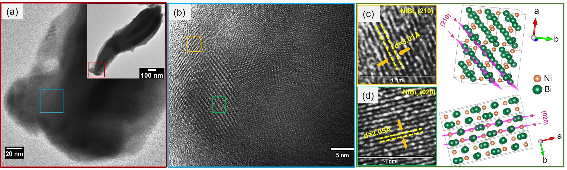
Figure 4(a) displays a TEM image of the zoomed region of the rod shown in the inset for the co-evaporated sample-C. Fig. 4(b) shows the HRTEM image of the blue square box and confirms the polycrystalline nature with different crystal orientations of the NiBi3 nanorod, grown during the room temperature co-evaporation at a Bi deposition rate of 0.8 Å/s. The most prominent crystal planes observed are (2 1 0) and (0 2 0) of NiBi3 marked in the yellow and green colored box. The zoom view of the fringe pattern of the yellow area has the nearest lattice plane distance of 3.01 Åfor (210) plane of NiBi3 along (001) zone axis. The corresponding schematic atomic model of the (210) lattice plane along (001) zone axis using the VESTA program33 is shown on the right side of Fig. 4(c). The zoomed fringe pattern of the green area corresponds to the (020) plane of NiBi3, with the nearest lattice plane distance of 2.01 Å. The schematic atomic model of the (020) lattice plane along the (001) zone axis is shown on the right side of the (020) fringe pattern. Both the lattice planes corroborate with the GIXRD peak shown in Fig. 1(d).
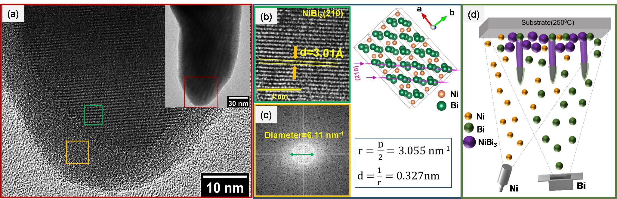
Similarly, Fig. 5(a) shows the HRTEM image of the nanowire formed on a co-evaporated sample deposited at an elevated temperature of 250 0C (sample-E). Inset shows a part of a single nanowire of length 13 m. We notice a clear single crystalline tip encompassed by an amorphous layer. A comparatively smaller crystalline region, marked by a green square, has been magnified in Fig. 5(b) to get precise information regarding the interplanar spacing. Here it is prominently visible that the nanowire is single crystalline. The zoomed view of the HRTEM shown in Fig. 5(b) represents the (2 1 0) planes of NiBi3 along the (001) zone axis with the nearest lattice plane distance of 3.01 Å. This NiBi3 plane (210) matches with the GIXRD plot in Fig. 2(c), corresponding to the 2-theta 29.623∘. The structural atomic representation of the planes is shown by the side of the fringe pattern. Fig. 5(c) is the fast Fourier transform (FFT) of the selected area in yellow square box Fig. 5(a) which falls in the amorphous cap region. The ring-like FFT pattern shows the amorphous nature on the cap region of the nanowire. The d value, calculated from the diameter of the ring is 0.327 nm, which matches with the Bi (012) hexagonal symmetry phase. This peculiar feature at the tip of the nanowire indicates that there is a similarity in the formation of these nanowires with the well-known vapor-liquid-solid (VLS) mechanism of nanowire growth. In this mechanism, a molten metal nanoparticle works as a catalyst and promotes anisotropic growth38, 39, 40, 41 in presence of a chemical vapor at high temperatures. Typically the molten metal catalyst remains as a cap at the top of the nanowires. The observed amorphous Bi cap, in our case, is very similar in nature42, 43, 44, 45. During the co-evaporation process, some Ni and Bi can interact in the vapor phase to form NiBi3. In addition, some excess Bi vapor and Ni vapor also reach the surface of the substrate. Due to the low melting point of Bi, the Bi vapor reaching at the heated substrate can be extremely mobile mimicking a liquid phase. Further, Ni and NiBi3 coming in contact with the apparent molten phase of Bi get catalyzed in the same manner as in VLS growth of nanowires in presence of Au droplets46, 47.
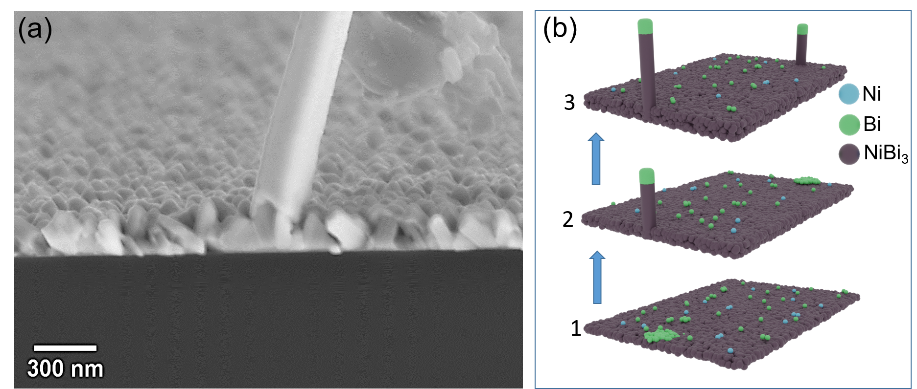
The schematic representation of the co-evaporation process (at substrate temperature 250∘C) that results in the formation of nanowires with a Bi cap at the tip is shown in Figure 5(d). The green cap at the tip is similar to the amorphous Bi cap shown in HRTEM fig-5 (a). We want to highlight here that, in the present case, the NiBi3 nanowires are much longer (10-25 m) than the earlier literature and are single crystalline in nature when grown at 250∘C. Our observations show a clear systematism in the deposition parameters for congruent, anisotropic growth of the nanorods on the film surface. Firstly, the dependence on Bi evaporation rate (in Fig 1) shows that relatively higher concentration of Bi in the co-evaportation flux promote nucleation of NiBi3 rods, albeit polycrystalline in nature. At higher evaporation rate of Bi, the chances of forming clusters/islands of pure Bi is higher. Therefore, it is very likely that the pure Bi clusters are the points of nucleation of the nanorods. This can be supported by the fact that TEM imaging shows amorphous Bi regions at the tip of the nanorods, especially well defined for the crystalline nanorods. Secondly, the temperature dependence (in Fig 2) shows that elevated temperature promotes crystalline nanorods. The average length of the crystalline nanorods was observed to be much higher than the polycrystalline rods obtained at lower temperatures. Therefore, substrate temperature strongly accelerates the anisotropic growth of rods. Since 250∘C is very close to the melting temperature of Bi, we believe that almost molten form of Bi clusters triggers the strongly anisotropic growth of NiBi3 nanorods. A cross sectional FESEM image of sample-E (with very long crystalline NiBi3 nanorods) is shown in Fig 6 (a). Clearly the nanorods seems to have started from the very base of the film. Based on these observations a plausible growth model of the nanowires is shown in the Fig 6(b). In the initial stages of the film growth, some clusters of Bi may appear on the surface. At growth temperatures close to the melting temperature of Bi, these clusters may act as very effective nucleation points for crystallization of NiBi3 nanorods. The fact that we see an amorphous Bi cap at the tip of the nanorods says that the NiBi3 crystallizes at the bottom of the molten Bi clusters formed in the initial stage of film growth. Usually, evaporation flux arriving on a substrate migrate on the surface to spread out as a thin film, However, the evaporation flux (Bi, Ni, and NiBi3) arriving on almost molten Bi regions gets captured in it and helps the crystallization of NiBi3 at the bottom of the cluster, very similar to the VLS mechanism widely used in the CVD growth of long semiconducting nanowires.
3.3.2 Superconductivity in single crystalline NiBi3 nanowire
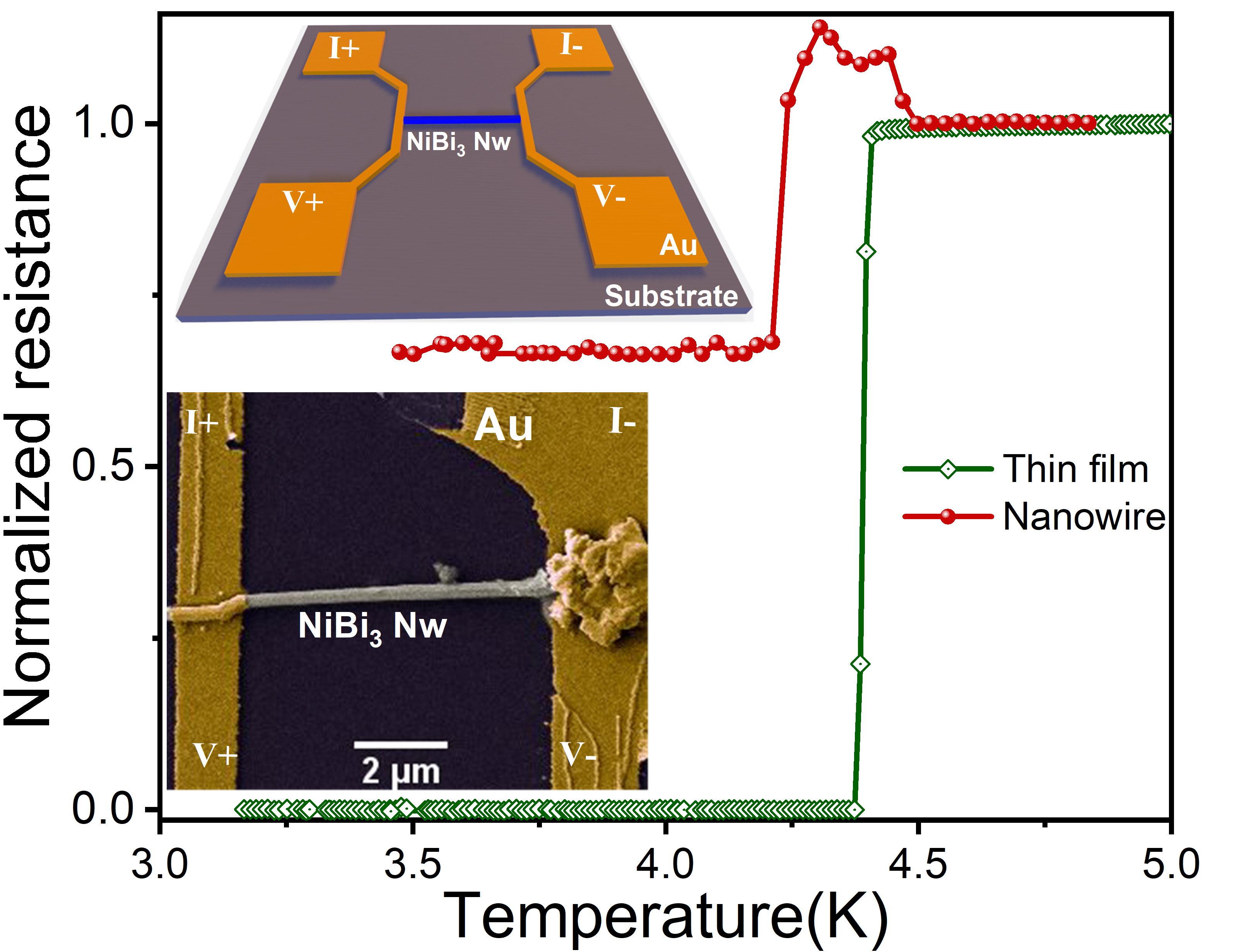
From the analysis of SEM and HRTEM data, we find that the NiBi3 nanowires obtained at a substrate temperature of 250∘ C are exceptionally long and single crystalline in nature. In this section, we verify the superconducting transition temperature of a single NiBi3 nanowire produced during the growth of the NiBi3 film at high temperature. For this purpose, we scratched the nanowires from the film surface onto a Si wafer coated with a 300 nm thick thermal oxide layer. Gold contact pads of 100 nm thickness were lithographically patterned at the two ends of a suitably placed NiBi3 nanowire (width 350 nm, length=12 m). A schematic diagram of the arrangement is shown in the inset of Fig-7. A false-color FESEM image of the actual nanowire with contact pads is also shown in the inset of the same figure. This arrangement allowed direct four-probe resistance measurement of the nanowire down to a temperature of 2 K. In the main panel of Fig-7, we compare the low-temperature resistances, normalized with the resistance at 4.75 K, of the film and the 12 m long nanowire obtained from the same film. A bias current of 10 A was used for both measurements. The thin film shows a clear and sharp superconducting transition at 4.4 K with a transition width of 0.05 K. The nanowire also shows a sharp transition at 4.3 K with a transition width of 0.1 K, although the resistance below the transition did not attain a zero value. This resistive nature of the nanowire is, however, a very well-known effect arising from the phase slips phenomenon in superconducting nanowires48, 49. Phase slip is a process by which the phase of the superconducting order parameter locally undergoes a sudden change by multiples of 2, which momentarily creates a normal region in the nanowire. Therefore, the average effect of multiple random phase-slip events appears as a resistance below the superconducting state, at any bias current48, 49. Therefore, the nanowires obtained during the film growth process have been verified as NiBi3 nanowires from both structural and from transport measurements.
4 Conclusion
In this article, we have discusses the growth of NiBi3 nanorods and nanowires during the co-evaporation of NiBi3 thin films. We find that the rate of evaporation of Bi and the substrate temperature, both significantly affect the growth of NiBi3 nanorods and nanowires. A relatively higher rate of evaporation of Bi and a relatively higher substrate temperature seemed favorable for the formation of the nanorods. From the glancing angle X-ray diffraction measurements, we found that the presence of the hexagonal-Bi is crucial for the nucleation of the nanorods. Although nanorods were also obtained at ambient substrate temperatures at a high rate of Bi evaporation, the nanowires obtained at a substrate temperature of 250o C, were single crystalline in nature. From HRTEM images we observed that the tip of the nanowires obtained at high substrate temperature was covered with a cap of amorphous Bi. This indicates that the formation of the nanowires is analogous to the well-known vapor-liquid-solid growth mechanism of nanowires in the CVD process. In this case, although there is no liquid state as such, the high mobility of the low melting point material Bi effectively plays the role of liquid and helps nucleate the long NiBi3 nanorods. It was found that the formation of nanowire occurs at random sites of the thin film with highly populated molten Bismuth relative to other spots, as seen in the cross-sectional FESEM image of the thin film. The superconducting transition of a single NiBi3 nanowire, measured by four probe method, was found to be 4.3 K, matching the transition temperature of single crystal NiBi3. In this work, we have identified the exact parameter window for the physical route fabrication of long, single crystal NiBi3 nanowires, which will open an opportunity for quantum transport measurements in nanowires of this interesting quantum system which is a superconductor based on a strong ferromagnetic material.
The authors would like to thank the National Institute of Science Education and Research (NISER), Department of Atomic Energy, Government of India, for funding the research work through project number RIN-4001. The authors would also like thank Mr. Ritarth Chaki for help with the 3D graphics.
References
- Nakamura 1995 Nakamura, M. Fundamental properties of intermetallic compounds. MRS Bulletin 1995, 20, 33–39
- Liu et al. 2018 Liu, L.; Xing, Y.; Merino, I.; Micklitz, H.; Franceschini, D.; Baggio-Saitovitch, E.; Bell, D.; Solórzano, I. Superconductivity in Bi/Ni bilayer system: Clear role of superconducting phases found at Bi/Ni interface. Physical Review Materials 2018, 2, 014601
- Şarlı and Keskin 2019 Şarlı, N.; Keskin, M. Coexistence of ferromagnetism and superconductivity in NiBi-binary alloy. Chinese Journal of Physics 2019, 60, 502–509
- Tencé et al. 2014 Tencé, S.; Janson, O.; Krellner, C.; Rosner, H.; Schwarz, U.; Grin, Y.; Steglich, F. CoBi3–the first binary compound of cobalt with bismuth: high-pressure synthesis and superconductivity. Journal of Physics: Condensed Matter 2014, 26, 395701
- Schwarz et al. 2013 Schwarz, U.; Tencé, S.; Janson, O.; Koz, C.; Krellner, C.; Burkhardt, U.; Rosner, H.; Steglich, F.; Grin, Y. CoBi3: A binary cobalt–bismuth compound and superconductor. Angewandte Chemie International Edition 2013, 52, 9853–9857
- Wei et al. 2016 Wei, X.-P.; Zhou, Y.-H.; Zhang, Y.-L. First-Principles Study the Electronic and Thermodynamic Properties for CoBi 3 Superconductor. Journal of Superconductivity and Novel Magnetism 2016, 29, 1203–1211
- Young et al. 1999 Young, B. A.; Saab, T.; Cabrera, B.; Cross, J.; Clarke, R.; Abusaidi, R. Measurement of T c suppression in tungsten using magnetic impurities. Journal of Applied Physics 1999, 86, 6975–6978
- Chen et al. 2008 Chen, X.; Wu, T.; Wu, G.; Liu, R.; Chen, H.; Fang, D. Superconductivity at 43 K in SmFeAsO1-xF x. nature 2008, 453, 761–762
- Kamihara et al. 2008 Kamihara, Y.; Watanabe, T.; Hirano, M.; Hosono, H. Iron-based layered superconductor La [O1-x F x] FeAs (x= 0.05- 0.12) with Tc= 26K. Journal of the American Chemical Society 2008, 130, 3296–3297
- Nedellec et al. 1985 Nedellec, P.; Creppy, F.; Dumoulin, L.; Burger, J. Anomalous electrical resistivity of Bi3Ni. Physics Letters A 1985, 111, 67–70
- Fujimori et al. 2000 Fujimori, Y.; Kan, S.-i.; Shinozaki, B.; Kawaguti, T. Superconducting and normal state properties of NiBi 3. Journal of the Physical Society of Japan 2000, 69, 3017–3026
- Kumar et al. 2011 Kumar, J.; Kumar, A.; Vajpayee, A.; Gahtori, B.; Sharma, D.; Ahluwalia, P.; Auluck, S.; Awana, V. Physical property and electronic structure characterization of bulk superconducting Bi3Ni. Superconductor Science and Technology 2011, 24, 085002
- Zhu et al. 2012 Zhu, X.; Lei, H.; Petrovic, C.; Zhang, Y., et al. Surface-induced magnetic fluctuations in a single-crystal NiBi 3 superconductor. Physical Review B 2012, 86, 024527
- Silva et al. 2013 Silva, B.; Luccas, R.; Nemes, N.; Hanko, J.; Osorio, M.; Kulkarni, P.; Mompean, F.; García-Hernández, M.; Ramos, M.; Vieira, S., et al. Superconductivity and magnetism on flux-grown single crystals of NiBi 3. Physical Review B 2013, 88, 184508
- Gonsalves et al. 2016 Gonsalves, S. H.; Opata, Y. A.; Pinheiro, L. B. L. G.; Leal, A. C. D. S.; Monteiro, J. F. H. L.; Siqueira, E. C.; de Andrade, A. V. C.; Jurelo, A. R. Superconductivity and magnetism in intermetallic Bi3Ni1- xFex superconductor. Solid State Communications 2016, 242, 6–10
- Piñeiro et al. 2011 Piñeiro, E. L. M.; Herrera, B. L. R.; Escudero, R.; Bucio, L. Possible coexistence of superconductivity and magnetism in intermetallic NiBi3. Solid State Communications 2011, 151, 425–429
- LeClair et al. 2005 LeClair, P.; Moodera, J. S.; Philip, J.; Heiman, D. Coexistence of Ferromagnetism and Superconductivity in Bilayers. Phys. Rev. Lett. 2005, 94, 037006
- Herrmannsdörfer et al. 2011 Herrmannsdörfer, T.; Skrotzki, R.; Wosnitza, J.; Köhler, . D.; Boldt, R.; Ruck, M. Structure-induced coexistence of ferromagnetic and superconducting states of single-phase Bi 3 Ni seen via magnetization and resistance measurements. Physical Review B 2011, 83, 140501
- Wang et al. 2023 Wang, J.; Farhang, C.; Yue, D.; Jin, X.; Zhu, X.; Xia, J. Absence of spontaneous time-reversal symmetry breaking and ferromagnetism in superconducting single crystal. Phys. Rev. B 2023, 107, 024415
- Sakurai et al. 2000 Sakurai, M. S. M.; Ono, T. O. T.; Yoshida, I. Y. I.; Tanuma, S. T. S. Thermoelectric and thermogalvanomagnetic properties of NiBi3. Japanese Journal of Applied Physics 2000, 39, 6366
- Siva et al. 2015 Siva, V.; Senapati, K.; Satpati, B.; Prusty, S.; Avasthi, D.; Kanjilal, D.; Sahoo, P. K. Spontaneous formation of superconducting NiBi3 phase in Ni-Bi bilayer films. Journal of Applied Physics 2015, 117, 083902
- Siva et al. 2016 Siva, V.; Pradhan, P. C.; Santosh Babu, G.; Nayak, M.; Sahoo, P. K.; Senapati, K. Superconducting proximity effect in NiBi3-Ni-NiBi3 trilayer system with sharp superconductor-ferromagnet boundaries. Journal of Applied Physics 2016, 119, 063902
- Bhatia et al. 2018 Bhatia, E.; Talapatra, A.; Mohanty, J. R.; Senapati, K. Superconductivity, Kondo effect, and observation of self-organized pattern formation in intermetallic NiBi3 thin films. Intermetallics 2018, 94, 160–164
- Siva et al. 2017 Siva, V.; Chettah, A.; Ojha, S.; Tripathi, A.; Kanjilal, D.; Sahoo, P. K. Interface mediated enhanced mixing of multilayered Ni-Bi thin films by swift heavy ion irradiation. Nuclear Instruments and Methods in Physics Research Section B: Beam Interactions with Materials and Atoms 2017, 409, 314–317
- Liu et al. 2020 Liu, L.; Xing, Y.; Merino, I.; Franceschini, D.; Solórzano, I.; Baggio-Saitovitch, E. Magnetic properties of superconducting phases NiBi and NiBi3 formed during pulsed laser deposition of Ni-Bi films. Journal of Magnetism and Magnetic Materials 2020, 514, 167275
- Vaughan et al. 2020 Vaughan, M.; Satchell, N.; Ali, M.; Kinane, C. J.; Stenning, G. B.; Langridge, S.; Burnell, G. Origin of superconductivity at nickel-bismuth interfaces. Physical Review Research 2020, 2, 013270
- Dybkov and Duchenko 1996 Dybkov, V.; Duchenko, O. Growth kinetics of compound layers at the nickel-bismuth interface. Journal of alloys and compounds 1996, 234, 295–300
- Das et al. 2023 Das, B.; Senapati, T. R.; Yadav, A. K.; Umapathy, G.; Jha, S. N.; Senapati, K.; Sahoo, P. K. Reaction-Diffusion-Driven Stoichiometric Gradient in Coevaporated Superconducting NiBi3 Thin Films. Crystal Growth & Design 2023,
- Mtshali et al. 2018 Mtshali, C.; Thethwayo, C.; Pineda-Vargas, C.; Ndwandwe, M. The effect of deposition rate and thermal annealing on morphology and microstructural evolution of Nickel-Bismuth thin film. Thin Solid Films 2018, 645, 312–319
- Liu et al. 2021 Liu, L.; Xing, Y.; Merino, I.; Henriques, M.; Doria, M.; Solórzano, I.; Baggio-Saitovitch, E. Spontaneous morphology and phase modification driven by sequence of deposition in superconducting Ni–Bi bilayers. Materials Chemistry and Physics 2021, 260, 124112
- Li et al. 2011 Li, C.; Mizuta, H.; Oda, S. Growth and characterisation of Ge Nanowires by chemical vapour deposition; InTech, 2011
- Iacopi et al. 2007 Iacopi, F.; Vereecken, P.; Schaekers, M.; Caymax, M.; Moelans, N.; Blanpain, B.; Richard, O.; Detavernier, C.; Griffiths, H. Plasma-enhanced chemical vapour deposition growth of Si nanowires with low melting point metal catalysts: an effective alternative to Au-mediated growth. Nanotechnology 2007, 18, 505307
- Momma and Izumi 2011 Momma, K.; Izumi, F. VESTA 3 for three-dimensional visualization of crystal, volumetric and morphology data. Journal of applied crystallography 2011, 44, 1272–1276
- Aousgi et al. 2015 Aousgi, F.; Dimassi, W.; Bessais, B.; Kanzari, M. Effect of substrate temperature on the structural, morphological, and optical properties of Sb2S3 thin films. Applied Surface Science 2015, 350, 19–24
- Balakrishnan et al. 2013 Balakrishnan, G.; Sundari, S. T.; Ramaseshan, R.; Thirumurugesan, R.; Mohandas, E.; Sastikumar, D.; Kuppusami, P.; Kim, T.; Song, J. Effect of substrate temperature on microstructure and optical properties of nanocrystalline alumina thin films. Ceramics International 2013, 39, 9017–9023
- Derby et al. 2018 Derby, B.; Cui, Y.; Baldwin, J.; Misra, A. Effects of substrate temperature and deposition rate on the phase separated morphology of co-sputtered, Cu-Mo thin films. Thin Solid Films 2018, 647, 50–56
- Jungyoon et al. 2003 Jungyoon, E.; Kim, S.; Lim, E.; Lee, K.; Cha, D.; Friedman, B. Effects of substrate temperature on copper (II) phthalocyanine thin films. Applied Surface Science 2003, 205, 274–279
- Hiruma et al. 1995 Hiruma, K.; Yazawa, M.; Katsuyama, T.; Ogawa, K.; Haraguchi, K.; Koguchi, M.; Kakibayashi, H. Growth and optical properties of nanometer-scale GaAs and InAs whiskers. Journal of Applied Physics 1995, 77, 447–462
- Wagner and Ellis 1964 Wagner, a. R.; Ellis, s. W. Vapor-liquid-solid mechanism of single crystal growth. Applied physics letters 1964, 4, 89–90
- Wang et al. 2006 Wang, B.; Yang, Y.; Xu, N.; Yang, G. Mechanisms of size-dependent shape evolution of one-dimensional nanostructure growth. Physical Review B 2006, 74, 235305
- Bonu et al. 2019 Bonu, V.; Sahu, B. K.; Das, A.; Amirthapandian, S.; Dhara, S.; Barshilia, H. C. Sub-wavelength waveguide properties of 1D and surface-functionalized SnO2 nanostructures of various morphologies. Beilstein journal of nanotechnology 2019, 10, 379–388
- Su et al. 2008 Su, Y.; Liang, X.; Li, S.; Chen, Y.; Zhou, Q.; Yin, S.; Meng, X.; Kong, M. Self-catalytic VLS growth and optical properties of single-crystalline GeO2 nanowire arrays. Materials Letters 2008, 62, 1010–1013
- Boulanger and Lapierre 2012 Boulanger, J.; Lapierre, R. Patterned gold-assisted growth of GaP nanowires on Si. Semiconductor Science and Technology 2012, 27, 035002
- Cui et al. 2013 Cui, H.; Sun, Y.; Wang, C. Unusual growth direction and controllable wettability of W-catalyzed AlN nanowires. CrystEngComm 2013, 15, 5376–5381
- Hatano et al. 2019 Hatano, K.; Kobayashi, K.; Hiraiwa, T.; Yoshida, T.; Yasuda, H.; Kokai, F. Germanium catalyzed vapor–liquid–solid growth and characterization of amorphous silicon oxide nanotubes: comparison to the growth of its nanowires. SN Applied Sciences 2019, 1, 1–13
- Hannon et al. 2006 Hannon, a. J.; Kodambaka, S.; Ross, F.; Tromp, R. The influence of the surface migration of gold on the growth of silicon nanowires. nature 2006, 440, 69–71
- Hijazi et al. 2020 Hijazi, H.; Leroy, F.; Monier, G.; Grégoire, G.; Gil, E.; Trassoudaine, A.; Dubrovskii, V. G.; Castelluci, D.; Goktas, N. I.; LaPierre, R. R., et al. Dynamics of gold droplet formation on SiO2/Si (111) surface. The Journal of Physical Chemistry C 2020, 124, 11946–11951
- Mooij and Nazarov 2006 Mooij, J.; Nazarov, Y. V. Superconducting nanowires as quantum phase-slip junctions. Nature Physics 2006, 2, 169–172
- Lau et al. 2001 Lau, C. N.; Markovic, N.; Bockrath, M.; Bezryadin, A.; Tinkham, M. Quantum phase slips in superconducting nanowires. Physical review letters 2001, 87, 217003