Qnami AG, 4132 Muttenz, Switzerland \alsoaffiliationSwiss Nanoscience Institute, University of Basel, 4056 Basel, Switzerland \alsoaffiliationSwiss Nanoscience Institute, University of Basel, 4056 Basel, Switzerland
Scanning NV magnetometry of focused-electron-beam-deposited cobalt nanomagnets
Abstract
Focused-electron-beam-induced deposition is a promising technique for patterning nanomagnets for spin qubit control in a single step. We fabricate cobalt nanomagnets in such a process, obtaining cobalt contents and saturation magnetizations comparable to or higher than those typically obtained using electron-beam lithography. We characterize the nanomagnets using transmission electron microscopy and image their stray magnetic field using scanning NV magnetometry, finding good agreement with micromagnetic simulations. The magnetometry reveals the presence of magnetic domains and halo side-deposits, which are common for this fabrication technique. Finally, we estimate dephasing times for electron spin qubits in the presence of disordered stray fields due to these side-deposits.
Nanomagnets with precisely defined geometries are of interest for a variety of applications, including magnetic resonance force microscopy1, 2, as mediating elements between spins and mechanical degrees of freedom3, 4, 5, magnetic memories6, and for the implementation of quantum logic with spin-based qubits7, 8 such as electron spins confined in quantum dots.
Such electron spin qubits can be controlled and manipulated using high-frequency voltages applied to metallic gates9, and selective spin rotation can be implemented by periodically displacing the electron wave function inside a magnetic field gradient resulting from a nearby nanomagnet 7. Recent experiments have shown successful operation in fault-tolerant regimes with gate fidelities above the required thresholds10, 11, 12. Realizing fast spin rotation, while at the same time keeping dephasing and relaxation rates acceptably low, requires precise engineering of strong magnetic field gradients. This places stringent constraints on the geometry, relative location and alignment, and magnetic properties of the used nanomagnets13, 14. Furthermore, when scaling up to larger qubit arrays, the variability between a large number of individual nanomagnets will need to be characterized and minimized. Spatial characterization of nanomagnet stray fields is therefore important in order to facilitate qubit device fabrication, precise positioning of quantum dots relative to the nanomagnet, and to correctly assess and minimize qubit decohering mechanisms.
Typically, nanomagnets are patterned using a multi-step procedure, involving resist-coating, electron-beam lithography, metallization, and lift-off. Such a procedure is prone to introducing impurities in the devices due to residual resist particles, as well as to introducing possible misalignment. Furthermore, such techniques are limited to fabrication of 2D patterns.
Here, we use focused-electron-beam-induced deposition (FEBID) to pattern Co nanomagnets in a single step15. FEBID is an appealing technique for the fabrication of nanomagnets integrated in qubit devices, since it generates no impurities in the form of residual resist, eases fabrication due to its single-step nature, and allows for the fabrication of 3D geometries16, opening up new ways of engineering magnetic gradients optimized for spin qubit control. FEBID of Co has been demonstrated as a reliable technique for growing highly magnetic nanostructures, reaching Co content of up to 96 atomic percent of bulk values17, 15. FEBID also allows for patterning with lateral resolution in the nm range18, approaching the intrinsic limit of the process imposed by the electron beam diameter19, 20. For Co nanostructures, lateral resolutions of below have thus far been achieved21.
We characterize the properties of FEBID nanomagnets using high-angle annular dark-field scanning transmission electron microscopy (HAADF-STEM), high-resolution energy dispersive spectroscopy (EDS) analysis, and atomic force microscopy (AFM). Next, We use scanning NV magnetometry (SNVM)22 to image the magnetic stray field of the Co deposits, both at externally applied magnetic field sufficiently high to achieve magnetization saturation, and at zero field. We find good agreement of our measurements with micromagnetic simulations.
From our SNVM measurements of the disordered magnetic stray field of unintended deposits surrounding the nanomagnet, we estimate spin qubit dephasing times in the presence of charge noise.
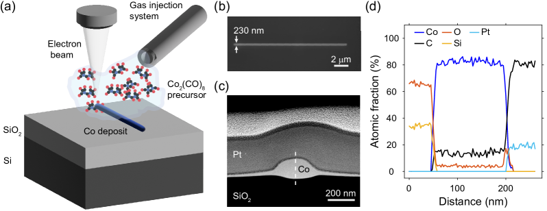
The sketch in Fig.1a illustrates the working principle of our FEBID23, 24, 25, 26 fabrication technique. First, a precursor molecule containing cobalt, , is introduced inside a chamber pumped to high vacuum. Irradiating the precursor with an electron beam causes it to decompose, leaving Co deposits on a nearby sample substrate15. By directing the beam using a scanning electron microscope, this technique can be used to, in a single step, pattern Co nanodeposits with high resolution21.
We use a Thermo Fisher FEI Helios 650 NanoLab FIB/SEM, fitted with a gas injection system. The nanomagnets are patterned on the top surface of a Si substrate covered with of thermally grown SiO. We fabricate the nanomagnets with a nanowire (NW) shape, in order to obtain a magnetic configuration with a single magnetic easy axis, enabling simple alignment of our scanning probe and straightforward comparison to simulations. To achieve high Co content and high lateral resolution, we used the following FEBID parameters15: an acceleration voltage of , a beam current of , a dwell time of , and a precursor flux corresponding to a vacuum chamber pressure of . Using these settings, we have achieved patterning Co structures with lateral widths down to and heights down to , as measured via AFM (See Supporting Information).
After FEBID fabrication, we use scanning and transmission electron microscopy (SEM and TEM) to characterize the geometry and composition of representative nanomagnets. Fig.1b shows an SEM top-view image of a Co NW deposit (dimensions: length, width, and height) and Fig.1c shows an HAADF-STEM image of a cross-section of such a deposit. In Fig.1c, the rounded cross-section of the Co NW can be discerned, as well as "halo" side-deposits of nm thickness extending laterally for several microns. EDS mapping along the linecut indicated in Fig.1c reveals a composition consisting mostly of Co (82 2.5 ), with additional smaller amounts of C (14 2.5 ) and O (4 2.5 ) (see Fig.1d). We find that this composition is rather uniform throughout the deposit, including similar proportions in the halo side-deposits (see Supporting Information for additional EDS data).
The halo is commonly deposited as a side-effect in FEBID, produced through precursor dissociation by secondary electrons scattering off the substrate and the pattern that is being grown27, 28. Such halo deposits are typically undesirable and various approaches can be used to mitigate their formation. The amount of halo and its composition can vary depending on the deposition parameters, in particular the exact amount of precursor gas present in the chamber. Furthermore, by performing FEBID at low temperatures, halo effects can potentially be reduced. Finally, the halo can in principle be removed by means of argon ion milling (see Supporting Information), although at the same time a layer of the intended deposited structure and surrounding substrate may be removed and charge defects may be introduced into the device.
Compared to other scanning probe magnetometry techniques29, such as scanning superconducting quantum interference device (SQUID) magnetometry and magnetic force microscopy (MFM), SNVM30, 2, 31 offers several advantages which make it suitable for our use. Of particular relevance for our application is the high spatial resolution that can be achieved with SNVM, which can reach 32, 33, 29, making it possible to image magnetic fields and currents at length scales relevant for spin qubit devices. Also, SNVM yields quantitative measurements of the magnetic fields as the Zeeman energy of a single NV-center defect can be probed directly. Furthermore, due to its high magnetic field sensitivity on the order of , SNVM allows imaging the weak fields associated with nanoscale magnetic domains 34 and other spatially inhomogeneous magnetic stray fields, making it a useful tool to study the magnetization properties of FEBID Co halo structures and their impact on spin qubit performance.
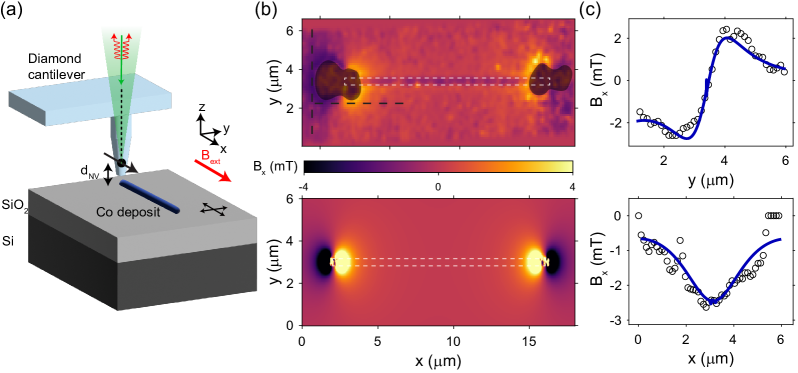
Fig.2a illustrates the SNVM setup employed here: a commercial system (Qnami ProteusQ) operating under ambient conditions. We use a diamond cantilever (Qnami Quantilever MX) hosting a single negatively charged NV center embedded inside its protruding tip. The cantilever is attached to a quartz Akiyama tuning fork, allowing for frequency-modulated AFM. For our measurements we use diamond tips hosting an NV center with a spin quantization axis oriented parallel to the principal axis of the NW magnet, i.e. along the -axis as defined in Fig.2a. This type of diamond tips are fabricated from 110 diamond blankets35. We estimate the distance of the NV center to the apex of the diamond tips to be 34, and corresponding best achievable lateral spatial resolutions of . During the measurements, an external magnetic field is applied along the NV quantization axis. This direction coincides with the principal NW axis and its easy magnetic axis. To perform magnetometry, we employ measurements of optically detected electron spin resonance as well as of fluorescence. See e.g. Celano et al.34 for a more in-depth description of the SNVM setup and measurement techniques used here.
Fig.2b shows an SNVM scan of a Co NW nanomagnet, taken with = , which falls within the typical operating range of spin qubits. The scan is taken with a tip-sample distance < , and consequently the magnetometry measurements are taken at a distance from the sample surface. The scan shows the -component of the magnetic stray field of the nanowire-shaped magnet, revealing a pole at each end of the magnet. At this value of , the nanomagnet is almost fully saturated along its magnetic easy axis. The associated stray field profile features large regions surrounding the nanomagnet where field components transverse to the quantization axis of the NV center are small. In these regions, relatively little quenching of NV fluorescence22 occurs and it is straightforward to reconstruct the -components of the stray field from the SNVM measurements. Even so, we blacked out regions in Fig.2b where we could not reliably track the Zeeman splitting of the NV center. This can occur when the magnetic stray field is too large, transverse components are too large, or when the optical read-out signal is quenched. Especially at the ends of the NW, we expect strong out-of-plane stray field components. These out-of-plane fields are transverse to the NV axis and lead to a quenching of the NV signal22.
We compare the SNVM measurement with finite-element simulations of the -component of the stray field in the same area around the NW (see Fig.2b, lower panel), using the software package MuMax3.36, 37 Here, we simulate the stray field of a rectangular Co box geometry with a width of , height of , and a length of . We use a typical value of the exchange constant for Co, , and a 5x5x5 nm3 cell size. Using this model, we obtain a stray field profile that qualitatively agrees well with the experiment, as shown in Fig.2b. Fig.2c shows plots of vertical and horizontal linecuts taken at the corresponding lines shown in Fig.2b. We find best agreement between simulation and experiment when we use a saturation magnetization of in the simulation. Such a saturation magnetization corresponds to 85% of the bulk value, agreeing well with the atomic fraction of Co measured in our deposit (Fig.1d). We note that exactly aligning the simulation with the experimental data in the -plane is to some degree hindered by imperfect knowledge of the precise location of the NV center inside the scanning tip, as well as by the pixel size of the scan. Some deviations between simulation and experiment may also result from the fact that in the simulation we do not take the rounded shape of the NW or the halo into account.
We further investigate the presence of magnetic structures of characteristic sizes of . Such dimensions are of the same order of magnitude as the length scales relevant for spin qubit devices, such as the typical dimensions of quantum dots, confinement gate electrodes, nanomagnets, and coupling elements9. Moreover, also tunneling lengths and typical wave function displacements are of a similar order of magnitude. Of particular relevance for spin qubits are unintended variations of the magnetic stray field on short length scales. In the presence of small displacements of the electron wave function, such variations can translate to magnetic noise, which can limit qubit decoherence 38, 14.
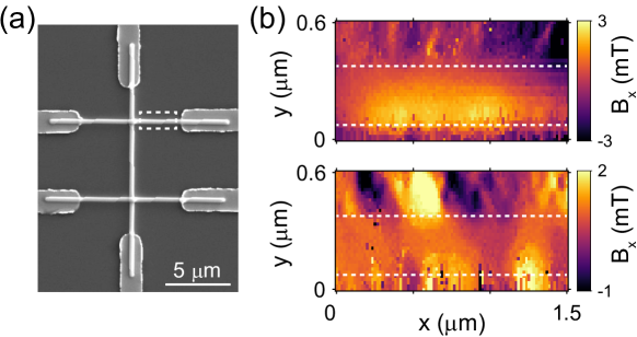
In the Co nanomagnet devices shown here, we find small magnetic structures in the form of magnetic domains inside the NW at low , as well as grain-like stray fields produced by the halo deposits surrounding the NW. We investigate these smaller structures in a Hall bar device consisting of 3 crossing Co NWs fabricated through FEBID using similar parameters as before, see Fig.3a. Fig.3b shows SNVM scans of a part of one of the Co NWs, in the region delineated in Fig.3a. In the upper panel of Fig.3b, SNVM data taken at = is shown, at which field the magnetization of the horizontal NW section is saturated, resulting in a homogeneous stray field above the NW. In the lower panel in Fig.3b, SNVM of the same section is shown at = . In this case, multiple domains of characteristic size of several hundred nanometer can be discerned in the observed stray field of the magnet including its halo.
Next, we use SNVM to study the halo side-deposits in more detail. Figs.4a, and b show optical microscopy and SNVM images, respectively, of a Co Hall bar structure patterned via FEBID, which exhibits a significant halo side deposit. As can be seen, the halo can be distinguished as a dark shade of inhomogeneous shape in the optical microscopy image. The SNVM image of the same area further reveals that the halo presents a magnetic stray field of grainy composition, see Fig.4b (see Supporting Information for a magnified figure). The grainy pattern follows the same shape as the dark shade discernible in Fig.4a: it surrounds the intended deposit and becomes smooth further away from the deposit. We investigate the size distribution of the grainy structures, using a segmentation analysis (Gwyddion) on a subset of the data shown in Fig.4b. We find a typical equivalent square side of roughly , larger than the pixel size of 50x50 nm of the scan. Furthermore, we find associated stray field fluctuations of up to 3 mT.
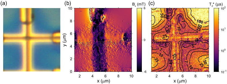
We estimate the effect of such magnetic stray field fluctuations on the dephasing of electron spin qubits when placed inside the stray field of Fig.4b. Specifically, we consider dephasing as a result of spin qubit displacements inside the halo stray field due to charge noise. Typical rms displacement amplitudes of QD electron spin qubits in this scenario are 14, 39, along and . Out-of-plane displacements are typically negligible for quantum well or MOS quantum dots, since the confinement potential in this direction is much larger than in the -plane. Since such displacements are orders of magnitude smaller than the grain size of the halo stray field, we can restrict our analysis to using the first derivative at each point, and neglect high-order derivatives of the stray field. Taking the spin qubit quantization axis to be parallel to , the stray field derivatives that are relevant for dephasing are therefore and . By differentiating the scan of Fig.4b with respect to and , we find that both and are largest for positions near the intended Co Hall bar deposit (top left and right corners, slightly above bottom left and right corners of plot in Fig.4b), but do not exceed 425T/nm at any point of the scan.
Using these derivatives of the stray field, we can estimate the inhomogeneous dephasing time of a spin qubit placed inside the grainy stray field induced by the halo. For each point of the scan of Fig.4b, we calculate using , with . Here we use 14, an electron spin Landé g-factor of 2, and we assume a quasi-static -like spectral density of the charge noise40. Fig.4c shows the corresponding map of . In this case, decreases from several hundreds of s on the bottom-right side of the scan, where almost no halo is present, to roughly in the top-left of the scan, where the halo is most intense. We find that exceeds for each point of the scan. Note that the contours in the plot of Fig.4c have been obtained by smoothing the data. While these contours indicate the trend of decreasing when approaching the Co deposit, the grainy pattern visible in the colorplot of Fig.4c originates from the disordered halo stray field, and hence should not be ignored.
The estimated shown in Fig.4e are on par with those found for various kinds of high-quality spin qubits in Si- and Ge-based quantum dots41, indicating that the spatially inhomogeneous stray fields of the halo side-deposits need not limit coherence more than other factors, such as charge noise in the presence of strong intended field gradients or spin-orbit coupling, and hyperfine interactions. In future work, we aim to characterize also the time-dependent magnetic noise originating from the halo and evaluate its impact on spin qubits. from Our TEM and SNVM characterization show that our FEBID structures have Co content and saturation magnetization comparable or higher than what is typically obtained using Co evaporation and standard electron beam lithography patterning. Moreover, past results have shown that depositions of Co content in excess of 95 atomic percent can be obtained using FEBID. Such high Co contents, in combination with the ability of FEBID to produce 3D magnet geometries would enable further optimization of nanomagnets for spin qubit control.
Finally, future research may target cryo-FEBID for the patterning of magnetic nanostructures on sensitive spin qubit devices, since it allows to pattern deposits with electron doses of order C/cm2, which is times less than needed for FEBID at room temperature42, 43, and similar to what is used in electron-beam exposure of resists. Hence, it can be expected that sample damage due to electron irradiation is comparable for cryo-FEBID and resist-based electron-beam lithography techniques.
We thank Prof. José María De Teresa, Prof. Patrick Maletinsky, and Dr. Monica Schönenberger for useful discussions and assisting with the AFM measurements. Calculations were performed at sciCORE (\urlhttp://scicore.unibas.ch) scientific computing center at University of Basel. We acknowledge funding from the Swiss National Science Foundation via NCCR SPIN as well as Project grant 200020_207933.
References
- Sidles et al. 1995 Sidles, J. A.; Garbini, J. L.; Bruland, K. J.; Rugar, D.; Züger, O.; Hoen, S.; Yannoni, C. S. Magnetic Resonance Force Microscopy. Reviews of Modern Physics 1995, 67, 249–265
- Degen et al. 2009 Degen, C. L.; Poggio, M.; Mamin, H. J.; Rettner, C. T.; Rugar, D. Nanoscale Magnetic Resonance Imaging. Proceedings of the National Academy of Sciences of the United States of America 2009, 106, 1313–1317
- Rabl et al. 2010 Rabl, P.; Kolkowitz, S. J.; Koppens, F. H. L.; Harris, J. G. E.; Zoller, P.; Lukin, M. D. A Quantum Spin Transducer Based on Nanoelectromechanical Resonator Arrays. Nature Physics 2010, 6, 602–608
- Gieseler et al. 2020 Gieseler, J.; Kabcenell, A.; Rosenfeld, E.; Schaefer, J. D.; Safira, A.; Schuetz, M. J. A.; Gonzalez-Ballestero, C.; Rusconi, C. C.; Romero-Isart, O.; Lukin, M. D. Single-Spin Magnetomechanics with Levitated Micromagnets. Physical Review Letters 2020, 124, 163604
- Rosenfeld et al. 2021 Rosenfeld, E.; Riedinger, R.; Gieseler, J.; Schuetz, M.; Lukin, M. D. Efficient Entanglement of Spin Qubits Mediated by a Hot Mechanical Oscillator. Physical Review Letters 2021, 126, 250505
- Slonczewski 1996 Slonczewski, J. C. Current-Driven Excitation of Magnetic Multilayers. Journal of Magnetism and Magnetic Materials 1996, 159, L1–L7
- Pioro-Ladrière et al. 2008 Pioro-Ladrière, M.; Obata, T.; Tokura, Y.; Shin, Y.-S.; Kubo, T.; Yoshida, K.; Taniyama, T.; Tarucha, S. Electrically Driven Single-Electron Spin Resonance in a Slanting Zeeman Field. Nature Physics 2008, 4, 776–779
- Tokura et al. 2006 Tokura, Y.; van der Wiel, W. G.; Obata, T.; Tarucha, S. Coherent Single Electron Spin Control in a Slanting Zeeman Field. Physical Review Letters 2006, 96, 047202
- Burkard et al. 2021 Burkard, G.; Ladd, T. D.; Nichol, J. M.; Pan, A.; Petta, J. R. Semiconductor Spin Qubits. arXiv:2112.08863 [cond-mat, physics:physics, physics:quant-ph] 2021,
- Mills et al. 2022 Mills, A. R.; Guinn, C. R.; Gullans, M. J.; Sigillito, A. J.; Feldman, M. M.; Nielsen, E.; Petta, J. R. Two-Qubit Silicon Quantum Processor with Operation Fidelity Exceeding 99%. Science Advances 2022, 8, eabn5130
- Noiri et al. 2022 Noiri, A.; Takeda, K.; Nakajima, T.; Kobayashi, T.; Sammak, A.; Scappucci, G.; Tarucha, S. Fast Universal Quantum Gate above the Fault-Tolerance Threshold in Silicon. Nature 2022, 601, 338–342
- Xue et al. 2022 Xue, X.; Russ, M.; Samkharadze, N.; Undseth, B.; Sammak, A.; Scappucci, G.; Vandersypen, L. M. K. Quantum Logic with Spin Qubits Crossing the Surface Code Threshold. Nature 2022, 601, 343–347
- Yoneda et al. 2015 Yoneda, J.; Otsuka, T.; Takakura, T.; Pioro-Ladrière, M.; Brunner, R.; Lu, H.; Nakajima, T.; Obata, T.; Noiri, A.; Palmstrøm, C. J.; Gossard, A. C.; Tarucha, S. Robust Micromagnet Design for Fast Electrical Manipulations of Single Spins in Quantum Dots. Applied Physics Express 2015, 8, 084401
- Neumann and Schreiber 2015 Neumann, R.; Schreiber, L. R. Simulation of Micro-Magnet Stray-Field Dynamics for Spin Qubit Manipulation. Journal of Applied Physics 2015, 117, 193903
- Teresa et al. 2016 Teresa, J. M. D.; Fernández-Pacheco, A.; Córdoba, R.; Serrano-Ramón, L.; Sangiao, S.; Ibarra, M. R. Review of Magnetic Nanostructures Grown by Focused Electron Beam Induced Deposition (FEBID). Journal of Physics D: Applied Physics 2016, 49, 243003
- Magén et al. 2021 Magén, C.; Pablo-Navarro, J.; De Teresa, J. M. Focused-Electron-Beam Engineering of 3D Magnetic Nanowires. Nanomaterials 2021, 11, 402
- Fernández-Pacheco et al. 2009 Fernández-Pacheco, A.; Teresa, J. M. D.; Córdoba, R.; Ibarra, M. R. Magnetotransport Properties of High-Quality Cobalt Nanowires Grown by Focused-Electron-Beam-Induced Deposition. Journal of Physics D: Applied Physics 2009, 42, 055005
- van Kouwen et al. 2009 van Kouwen, L.; Botman, A.; Hagen, C. W. Focused Electron-Beam-Induced Deposition of 3 Nm Dots in a Scanning Electron Microscope. Nano Letters 2009, 9, 2149–2152
- Silvis-Cividjian et al. 2005 Silvis-Cividjian, N.; Hagen, C. W.; Kruit, P. Spatial Resolution Limits in Electron-Beam-Induced Deposition. Journal of Applied Physics 2005, 98, 084905
- Salvador-Porroche et al. 2021 Salvador-Porroche, A.; Sangiao, S.; Magén, C.; Barrado, M.; Philipp, P.; Belotcerkovtceva, D.; Venkata Kamalakar, M.; Cea, P.; Teresa, J. M. D. Highly-Efficient Growth of Cobalt Nanostructures Using Focused Ion Beam Induced Deposition under Cryogenic Conditions: Application to Electrical Contacts on Graphene, Magnetism and Hard Masking. Nanoscale Advances 2021, 3, 5656–5662
- Serrano-Ramón et al. 2011 Serrano-Ramón, L.; Córdoba, R.; Rodríguez, L. A.; Magén, C.; Snoeck, E.; Gatel, C.; Serrano, I.; Ibarra, M. R.; De Teresa, J. M. Ultrasmall Functional Ferromagnetic Nanostructures Grown by Focused Electron-Beam-Induced Deposition. ACS Nano 2011, 5, 7781–7787
- Rondin et al. 2014 Rondin, L.; Tetienne, J.-P.; Hingant, T.; Roch, J.-F.; Maletinsky, P.; Jacques, V. Magnetometry with Nitrogen-Vacancy Defects in Diamond. Reports on Progress in Physics 2014, 77, 056503
- Randolph et al. 2006 Randolph, S. J.; Fowlkes, J. D.; Rack, P. D. Focused, Nanoscale Electron-Beam-Induced Deposition and Etching. Critical Reviews in Solid State and Materials Sciences 2006, 31, 55–89
- Utke et al. 2008 Utke, I.; Hoffmann, P.; Melngailis, J. Gas-Assisted Focused Electron Beam and Ion Beam Processing and Fabrication. Journal of Vacuum Science & Technology B: Microelectronics and Nanometer Structures Processing, Measurement, and Phenomena 2008, 26, 1197–1276
- Huth et al. 2012 Huth, M.; Porrati, F.; Schwalb, C.; Winhold, M.; Sachser, R.; Dukic, M.; Adams, J.; Fantner, G. Focused Electron Beam Induced Deposition: A Perspective. Beilstein Journal of Nanotechnology 2012, 3, 597–619
- Utke et al. 2012 Utke, I., Moshkalev, S., Russell, P., Eds. Nanofabrication Using Focused Ion and Electron Beams: Principles and Applications; Oxford University Press: Oxford, New York, 2012
- Gavagnin et al. 2014 Gavagnin, M.; Wanzenboeck, H. D.; Belic, D.; Shawrav, M. M.; Persson, A.; Gunnarsson, K.; Svedlindh, P.; Bertagnolli, E. Magnetic Force Microscopy Study of Shape Engineered FEBID Iron Nanostructures. physica status solidi (a) 2014, 211, 368–374
- Shawrav et al. 2016 Shawrav, M. M.; Taus, P.; Wanzenboeck, H. D.; Schinnerl, M.; Stöger-Pollach, M.; Schwarz, S.; Steiger-Thirsfeld, A.; Bertagnolli, E. Highly Conductive and Pure Gold Nanostructures Grown by Electron Beam Induced Deposition. Scientific Reports 2016, 6, 34003
- Marchiori et al. 2021 Marchiori, E.; Ceccarelli, L.; Rossi, N.; Lorenzelli, L.; Degen, C. L.; Poggio, M. Nanoscale Magnetic Field Imaging for 2D Materials. Nature Reviews Physics 2021, 1–12
- Degen 2008 Degen, C. L. Scanning Magnetic Field Microscope with a Diamond Single-Spin Sensor. Applied Physics Letters 2008, 92, 243111
- Schirhagl et al. 2014 Schirhagl, R.; Chang, K.; Loretz, M.; Degen, C. L. Nitrogen-Vacancy Centers in Diamond: Nanoscale Sensors for Physics and Biology. Annual Review of Physical Chemistry 2014, 65, 83–105
- Chang et al. 2017 Chang, K.; Eichler, A.; Rhensius, J.; Lorenzelli, L.; Degen, C. L. Nanoscale Imaging of Current Density with a Single-Spin Magnetometer. Nano Letters 2017, 17, 2367–2373
- Ariyaratne et al. 2018 Ariyaratne, A.; Bluvstein, D.; Myers, B. A.; Jayich, A. C. B. Nanoscale Electrical Conductivity Imaging Using a Nitrogen-Vacancy Center in Diamond. Nature Communications 2018, 9, 2406
- Celano et al. 2021 Celano, U.; Zhong, H.; Ciubotaru, F.; Stoleriu, L.; Stark, A.; Rickhaus, P.; de Oliveira, F. F.; Munsch, M.; Favia, P.; Korytov, M.; Van Marcke, P.; Maletinsky, P.; Adelmann, C.; van der Heide, P. Probing Magnetic Defects in Ultra-Scaled Nanowires with Optically Detected Spin Resonance in Nitrogen-Vacancy Center in Diamond. Nano Letters 2021, 21, 10409–10415
- Maertz et al. 2010 Maertz, B. J.; Wijnheijmer, A. P.; Fuchs, G. D.; Nowakowski, M. E.; Awschalom, D. D. Vector Magnetic Field Microscopy Using Nitrogen Vacancy Centers in Diamond. Applied Physics Letters 2010, 96, 092504
- Vansteenkiste et al. 2014 Vansteenkiste, A.; Leliaert, J.; Dvornik, M.; Helsen, M.; Garcia-Sanchez, F.; Van Waeyenberge, B. The Design and Verification of MuMax3. AIP Advances 2014, 4, 107133
- Exl et al. 2014 Exl, L.; Bance, S.; Reichel, F.; Schrefl, T.; Peter Stimming, H.; Mauser, N. J. LaBonte’s Method Revisited: An Effective Steepest Descent Method for Micromagnetic Energy Minimization. Journal of Applied Physics 2014, 115, 17D118
- Hanson et al. 2007 Hanson, R.; Kouwenhoven, L. P.; Petta, J. R.; Tarucha, S.; Vandersypen, L. M. K. Spins in Few-Electron Quantum Dots. Reviews of Modern Physics 2007, 79, 1217–1265
- Kawakami et al. 2014 Kawakami, E.; Scarlino, P.; Ward, D. R.; Braakman, F. R.; Savage, D. E.; Lagally, M. G.; Friesen, M.; Coppersmith, S. N.; Eriksson, M. A.; Vandersypen, L. M. K. Electrical Control of a Long-Lived Spin Qubit in a Si/SiGe Quantum Dot. Nature Nanotechnology 2014, 9, 666–670
- Nakajima et al. 2020 Nakajima, T.; Noiri, A.; Kawasaki, K.; Yoneda, J.; Stano, P.; Amaha, S.; Otsuka, T.; Takeda, K.; Delbecq, M. R.; Allison, G.; Ludwig, A.; Wieck, A. D.; Loss, D.; Tarucha, S. Coherence of a Driven Electron Spin Qubit Actively Decoupled from Quasistatic Noise. Physical Review X 2020, 10, 011060
- Stano and Loss 2022 Stano, P.; Loss, D. Review of Performance Metrics of Spin Qubits in Gated Semiconducting Nanostructures. Nature Reviews Physics 2022, 4, 672–688
- Bresin et al. 2013 Bresin, M.; Toth, M.; Dunn, K. A. Direct-Write 3D Nanolithography at Cryogenic Temperatures. Nanotechnology 2013, 24, 035301
- De Teresa et al. 2019 De Teresa, J. M.; Orús, P.; Córdoba, R.; Philipp, P. Comparison between Focused Electron/Ion Beam-Induced Deposition at Room Temperature and under Cryogenic Conditions. Micromachines 2019, 10
- Balasubramanian et al. 2008 Balasubramanian, G.; Chan, I. Y.; Kolesov, R.; Al-Hmoud, M.; Tisler, J.; Shin, C.; Kim, C.; Wojcik, A.; Hemmer, P. R.; Krueger, A.; Hanke, T.; Leitenstorfer, A.; Bratschitsch, R.; Jelezko, F.; Wrachtrup, J. Nanoscale Imaging Magnetometry with Diamond Spins under Ambient Conditions. Nature 2008, 455, 648–651