Mode-locked laser in nanophotonic lithium niobate
Abstract
Mode-locked lasers (MLLs) have enabled ultrafast sciences and technologies by generating ultrashort pulses with peak powers substantially exceeding their average powers. Recently, tremendous efforts have been focused on realizing integrated MLLs not only to address the challenges associated with their size and power demand, but also to enable transforming the ultrafast technologies into nanophotonic chips, and ultimately to unlock their potential for a plethora of applications. However, till now the prospect of integrated MLLs driving ultrafast nanophotonic circuits has remained elusive because of their typically low peak powers, lack of controllability, and challenges with integration with appropriate nanophotonic platforms. Here, we overcome these limitations by demonstrating an electrically-pumped actively MLL in nanophotonic lithium niobate based on its hybrid integration with a III-V semiconductor optical amplifier. Our MLL generates 4.8 ps optical pulses around 1065 nm at a repetition rate of 10 GHz, with pulse energy exceeding 2.6 pJ and a high peak power beyond 0.5 W. We show that both the repetition rate and the carrier-envelope-offset of the resulting frequency comb can be flexibly controlled in a wide range using the RF driving frequency and the pump current, paving the way for fully-stabilized on-chip frequency combs in nanophotonics. Our work marks an important step toward fully-integrated nonlinear and ultrafast photonic systems in nanophotonic lithium niobate.
Mode-locked lasers (MLLs), which generate intense and coherent ultrashort optical pulses on picosecond and femtosecond timescales, have enabled numerous sciences and technologies in photonics such as extreme nonlinear optics1, femtochemistry2, supercontinuum generation3, optical atomic clocks 4, 5, optical frequency combs6, biological imaging7, 8, and photonic computing9. Today’s state-of-the-art MLLs are based on discrete fiber-based and free-space optical components and are expensive, power-demanding, and bulky. Realizing MLLs on integrated photonic platforms promises widespread utilization of ultrafast photonic systems which are currently limited to table-top laboratory experiments. However, so far the performance of integrated MLLs has not been on par with their table-top counterparts, lacking the required peak intensities and degrees of controllability required for on-chip ultrafast optical systems10, and many of the high-performance MLLs are not yet integratable with nanophotonic platforms. A major challenge lies in the simultaneous realization of large laser gain and an efficient mode-locking mechanism on integrated photonic platforms. Although III-V semiconductor gain media can be electrically pumped and they generally exhibit a very high gain per unit length and high saturation powers11, the conventional method of achieving mode-locking and short pulse generation on the same semiconductor chip requires a narrow range of pumping current, thus significantly limiting the output power and the tunability of the integrated MLLs12, 13, 14.
To realize high-peak-power integrated MLLs, a promising approach consists of the hybrid integration of a semiconductor gain medium and an external mode-locking element based on electro-optic (EO) or nonlinear optical effects. Recently, thin-film lithium niobate (TFLN) has emerged as a promising integrated nonlinear photonic platform with access to power-efficient and high-speed EO modulation15, 16 and strong quadratic () optical nonlinearity17, 18. Hybrid integration of semiconductor gain with TFLN enables a strong interplay between the laser gain and the EO or nonlinear effects to achieve active or passive mode-locking with high efficiency and tunability. Moreover, many of the nonlinear and ultrafast optical functionalities such as supercontinuum generation19, optical parametric oscillation20, 21, 22, 23, pulse shortening24, all-optical switching25, and quantum squeezing26 can be realized in quasi-phase-matched LN nanophotonic devices with orders of magnitude lower peak powers compared to other platforms. Therefore, developing high-peak-power MLLs integrated into nanophotonic LN can enable a suite of nonlinear and ultrafast optical phenomena on a chip, promising integrated photonic systems with unprecedented performance and functionalities.
In this work, we demonstrate a high-peak-power, electrically-pumped integrated actively MLL by hybrid integration of III-V semiconductors and LN nanophotonics. In contrast to conventional integrated MLLs based on hybrid integration of a III-V active region and a passive waveguide10, 12, our MLL synergistically exploits the high laser gain of III-V semiconductors and the efficient active optical phase modulation in LN nanophotonic waveguides as the mode-locking mechanism. Such a design eliminates the complexities associated with realizing gain and saturable absorption on the same semiconductor chip, allowing a much higher output power and a wider tunability of the laser. Under an external RF drive of less than 300 mW, our MLL generates ultrashort optical pulses around 1065 nm with a pulse duration of approximately 5 ps, pulse energy greater than 5 pJ, and a peak power greater than 0.5 W. This represents the highest reported peak power at a repetition rate of 10 GHz for integrated MLLs in nanophotonics. The MLL can operate over a broad range of electrical pumping currents and RF driving frequencies, and provide precise control of the carrier frequency and repetition rate of the resulting frequency comb, which can lead to fully-stabilized comb sources. In contrast to other recent demonstrations of ultrashort pulse sources on the TFLN platform such as Kerr soliton micro-combs27, 28 and electro-optic (EO) combs29, 30, 31, our MLL provides significantly higher on-chip peak power and pulse energies, and electrical-to-short-pulse efficiencies. Moreover, our MLL offers great system simplicity by eliminating the need for wavelength-tunable pump lasers, external optical amplification stages, complex cavity locking schemes, and/or pulse compression elements with high optical loss. The simplicity of our MLL design, combined with its high peak power, few-picosecond pulses, and controllable frequency comb parameters offers a practical path for fully-integrated nonlinear and ultrafast photonic systems in LN nanophotonics.
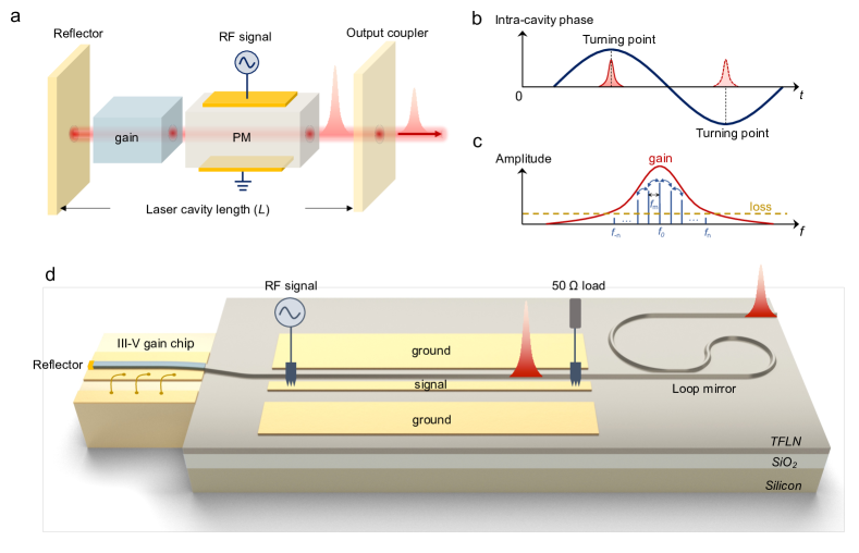
Operating principle and design of the MLL: Figure 1a shows the concept of active mode-locking by electro-optic phase modulation inside a laser cavity. In the time domain, when a phase modulator (PM) is driven by a sinusoidal RF signal at a frequency , the intra-cavity phase modulation is equivalent to the cavity length modulation. Therefore, the laser cavity can be considered as having a moving end mirror with a sinusoidal motion at frequency . When an optical signal inside the cavity strikes this moving end mirror and gets reflected back, its optical frequency acquires a Doppler shift. After successive round trips, these Doppler shifts will accumulate, resulting in no steady-state solution. However, when a short circulating pulse strikes the end mirror at either of the “turning points” where the mirror reverses its direction (the extremum of the phase variation as shown in Fig. 1b), it will not acquire a Doppler frequency shift but instead a small quadratic phase modulation or chirp32, 31. Thus, an optical pulse can be maintained in the laser cavity after successive round trips as a steady-state solution. The characteristics of the pulse depend on the gain, loss, and dispersion in the cavity as well as the chirp from the PM. While in principle optical pulses can occur at either of the two phase modulation extrema and acquire chirp of different signs, the dispersion in the cavity can compensate for the chirp imposed by the PM at one extremum, and further chirp the pulse formed at another extremum. As a result, the combination of dispersion, gain, and nonlinear effect in the cavity can favor one pulse over the other, leading to only one pulse in the cavity33. Such a mode-locking condition necessitates a good match between the phase modulation time period and the cavity round-trip time ( should be close to the cavity free spectral range (FSR)). The mode-locking mechanism can also be understood in the frequency domain. As shown in Fig. 1c, if the intra-cavity phase modulation frequency matches the cavity FSR, the sidebands produced by each of the running axial modes are injected into the adjacent axial modes, resulting in the phase locking of adjacent modes. While the mutual injection of spectral modes within the cavity bears similarity to EO comb sources, it is important to note that in MLLs, these modes will lase due to the presence of laser gain within the cavity, whereas in EO comb sources, they are generated by dispersing the energy from a single pump laser line29, 31, 30, 34. This distinction gives rise to stark differences in their operations.
Based on this principle, we design the integrated actively MLL as shown in Figure 1c. In our MLL, an electrically pumped gain section based on a single-angled facet GaAs gain chip (SAF gain chip) is butt-coupled to a TFLN chip, which contains an integrated EO phase modulator (PM) and a broadband loop mirror. A Fabry-Perot laser cavity configuration is formed between the reflective facet on the left end of the SAF gain chip and the broadband loop mirror on the TFLN chip. Here, an integrated PM is preferred over a Mach Zehnder interferometer (MZI)-based intensity modulator (IM) because the PM offers a lower insertion loss and avoids effects from the DC bias drift of the MZI modulator35. Thus, our MLL principle is distinct from that of an actively MLL based on an IM, in which the mode-locking is enabled by loss modulation36. It is worth noting that semiconductor gain medium typically has a short carrier relaxation time (gain recovery time ()) on the order of ns11, 37, 36. To ensure the mode-locking and the formation of ultrashort optical pulses, has to exceed the cavity round-trip time () of pulses by a large amount ()36. In our design, by controlling the length of the TFLN waveguide, we realized this condition by having a cavity FSR of GHz, which translates to a cavity round-trip time of ps.
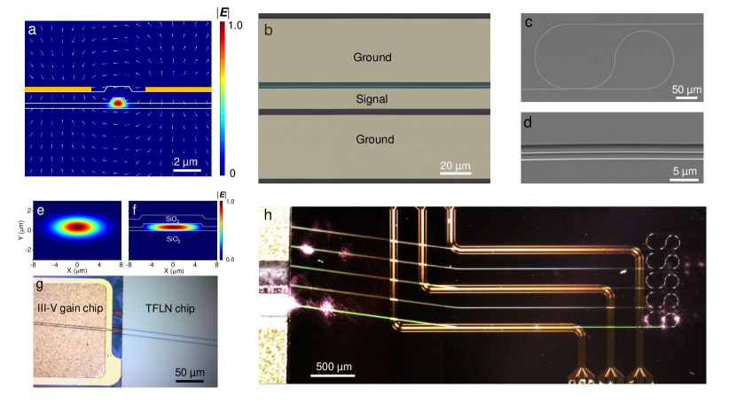
We fabricated our devices on a 700-nm-thick X-cut magnesium-oxide (MgO) doped TFLN on a SiO2/Silicon (4.7 m/500 m) substrate (NANOLN). The details about the device fabrication can be found in the Methods. As shown in Fig. 2a, in the PM region, the RF electrodes are fabricated on top of the SiO2 cladding layer. Such a design allows us to achieve high modulation efficiency (simulated value of 1.1 V cm) by having a small gap (4 m here) between the ground and signal electrodes and a significant overlap between the RF field and the optical field in the waveguide16, 38. It also ensures a low optical propagation loss by offering a high tolerance to misalignment between the electrodes and the optical waveguide16. We designed the geometry of the RF electrode to ensure a 50 impedance around 10 GHz. Figures 2b, c, and d show the scanning electron microscope (SEM) images of the PM and the loop mirror regions of the fabricated device. In the loop mirror, we adopted a curved coupling region design39 which increases the reflective bandwidth. The detailed design of the broadband loop mirror is described in the Supplementary Information Section II. Based on the length (1.5 mm) and the refractive index of the SAF gain chip around 1065 nm, we estimate that a 3-mm-long TFLN waveguide can lead to a laser cavity FSR of 10 GHz.
Figure 2e shows the 1065-nm fundamental TE mode profile in the waveguide of the SAF gain chip, which is calculated from the divergence angle of its emission. To minimize the coupling loss between the SAF gain chip and the TFLN chip, the top width of the input facet of the TFLN waveguide is tapered out to be 10.3 m. The 1065-nm fundamental TE mode profile in the tapered TFLN waveguide is shown in Fig. 2f. This design ensures a maximal overlap with the optical mode produced by the SAF gain chip and yields a minimal coupling loss of 1.5 dB. In Section I of the Supplementary Information, we discuss the dependence of coupling loss on the lateral misalignment and gap between the SAF gain chip and TFLN waveguides. The coupling loss can be further reduced by employing a polymer-based mode-size converter40. Fig. 2g shows the microscope image of the coupling region after the alignment, in which the gap between the two chips is minimized. When the SAF gain chip is electrically pumped with a driving current () of 160 mA, we observe green light (the second harmonic of the 1065 nm light) inside the laser cavity (Fig. 1h), which indicates a high intra-cavity power around 1065 nm and a good alignment between the two chips.
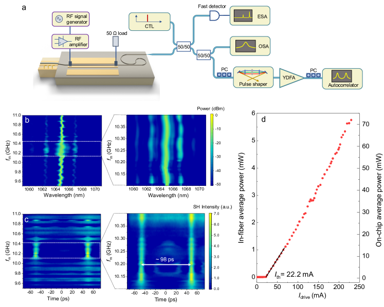
Characterization of the MLL: We characterized the integrated actively MLL using an optical setup shown in Fig. 3a. We applied a 280 mW sinusoidal RF signal to the left end of the traveling wave electrodes (TWE) of the PM by the RF probe. The right end of the TWE is terminated by another RF probe with a 50 load resistor mounted on it. To investigate the operating regimes of the MLL, we simultaneously collect the laser output spectra, the intensity autocorrelation of the laser output in the time domain, and the heterodyne beat notes between two neighboring laser emission lines and a narrow-linewidth (10 kHz) reference CW tunable laser (CTL, Toptica). In order to get intensity autocorrelation with a good signal-to-noise ratio, we pre-amplified the laser output power by a Ytterbium-doped fiber amplifier (YDFA). We also used a pulse shaper (Waveshaper 1000A, II-VI) to compensate for the group velocity dispersion (GVD) imposed by the phase modulator, YDFA, and the single-mode fiber. In the measurement, the gain chip is electrically pumped with an of 185.2 mA.
As shown in Fig. 3b, when we widely scan the , the laser output exhibits a clear spectral broadening when is between 10.1 and 10.4 GHz (labeled by the white dashed box). Meanwhile, within this range, two distinct intensity autocorrelation peaks separated by 98 ps emerge (Fig. 3c), which indicates that optical pulses are formed in this regime. At a of 10.17 GHz, we measured the laser output power from the output facet of the TFLN chip with a single-mode lensed fiber. As shown in Fig. 3 d, the laser exhibits a very low threshold of 22 mA. Given the measured coupling loss of 11 dB between the TFLN waveguide and the single-mode lensed fiber, the on-chip laser output average power is more than 50 mW when the is greater than 180 mA.
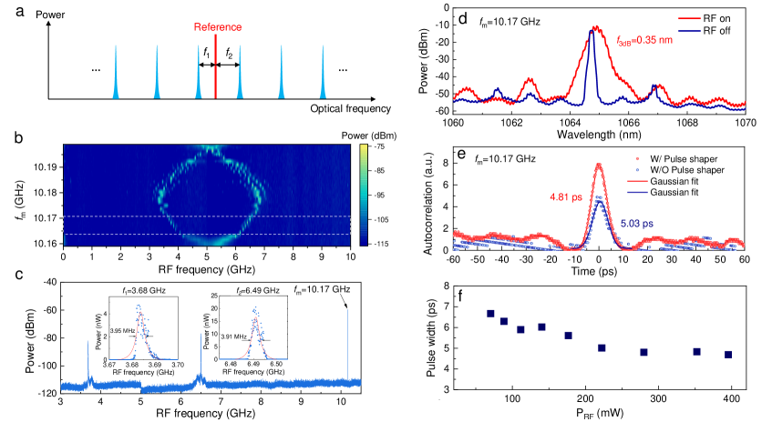
We further use the heterodyne beat notes to characterize the mode-locking and the resulting frequency comb. As illustrated in Fig. 4a, when the frequency of the reference CTL is resting in between the two neighboring comb lines of the MLL near the center of its spectrum, two RF beat notes at and are generated on the fast detector. Figure 4b shows the evolution of heterodyne beat notes as a function of . When is between 10.165 and 10.173 GHz as labeled by the white dashed box, two spectrally narrow beat notes are observed. This suggests that within this range of , the laser is operating in the mode-locked regime so that neighboring axial modes of the laser are phase-locked and it produces a frequency comb with narrow spectral peaks. In the time domain, this means a good synchronization between the round-trip of the pulse in the cavity and the phase modulation has been achieved, and the laser produces ultrashort optical pulses with high coherence.
We also want to comment on some of the important behaviors of the resulting frequency comb when is detuned from the cavity FSR. First, when the detuning is small (10.165 GHz<<10.173 GHz), we can still get two narrow beat notes, but and can shift significantly with , as shown in Fig. 4b. This indicates that the carrier frequency of the MLL sensitively depends on . Second, when the is further detuned from the cavity FSR, the MLL exhibits a transition to a turbulent regime41, which is manifested by multiple noisy beat notes around and in Fig. 4b. In the turbulent regime, the MLL can no longer reach steady state. In this regime, the laser can still emit ultrashort pulses as shown in Fig. 3c, albeit with low coherence.
As shown in Fig. 4c, at =10.17 GHz, we obtained two spectrally narrow RF beat notes at =3.68 GHz and =6.49 GHz, with a full width at half maximum (FWHM) linewidth of 3.95 MHz and 3.91 MHz, respectively. Given that the RF drive has a very small phase noise and no active locking of the laser cavity is used here, the linewidths of the heterodyne beat notes can be mainly limited by the drift of pulse carrier frequency. As shown in Fig. 4d, when a 280 mW RF drive at 10.17 GHz is applied to the PM, significant spectral broadening is observed. The pulse spectrum is centered at 1064.9 nm and the FWHM of the spectrum is 0.35 nm. Meanwhile, we also collected the intensity autocorrelation of the MLL output at =10.17 GHz, as shown in Fig. 4e. The autocorrelation trace indicates that the MLL produces one strong pulse at one of the modulation turning points, while the other pulse is significantly suppressed. The Gaussian fit of the intensity autocorrelation trace yields a pulse width of 4.81 ps (5.03 ps) with (without) the external pulse shaping. Since the pulse shaper can compensate for the chirp on the output pulse and the additional chirp imposed by the SMF and the YDFA, we expect the output pulse width directly after the MLL facet to be between 4.81 ps and 5.03 ps. The pulse width of 4.81 ps after pulse shaping corresponds to a time-bandwidth product of 0.445, which is very close to the transform-limited time-bandwidth product (0.44) of a Gaussian pulse42. To conservatively estimate the pulse energy and peak power, we use the measured output average power of 53 mW at mA and assume both pulses exist in the cavity. Hence, the output pulse energy of our MLL is at least 2.6 pJ and the pulse peak power is greater than 0.51 W.
We further studied the limits of the output pulse width of our MLL. First, we measured how the pulse width changes with the RF power ( applied to the PM. As shown in Fig. 4f, the measured pulse only slightly decreases with increasing , which is in good agreement with the power scaling law according to the Haus Master Equation (HME)43. We also found that further increasing the RF power will not shorten the pulse significantly. Instead, it can lead to laser instability due to index modulation of the TFLN waveguide caused by RF heating. By using the HME and ignoring the GVD and nonlinear effects in the laser cavity, we estimate that the pulse width limit of our actively MLL is 2.3 ps (see Supplementary Information Section IV for details). The experimentally measured pulse width is wider likely due to several factors, including cavity GVD, and the self-phase modulation and nonlinear chirp of the pulses imposed by the dynamical refractive index variation of the III-V gain medium associated with gain depletion and partial gain recovery11.
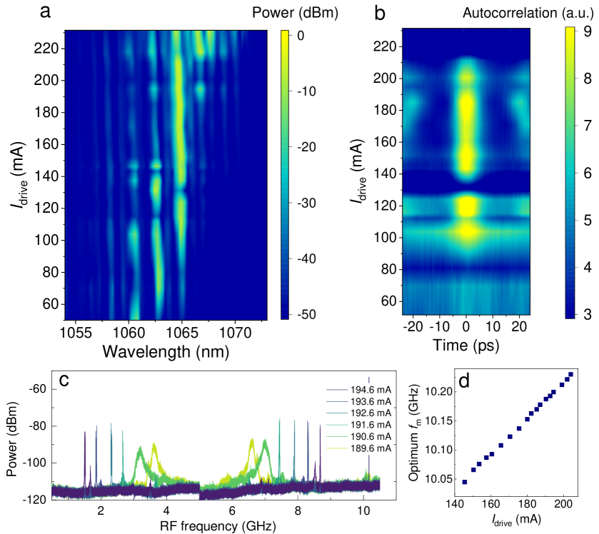
Current tuning of the MLL: The electrical pumping current of the III-V gain chip () can serve as an important tuning knob of our MLL. Since can alter the gain spectrum and the refractive index of the gain medium, it can in turn vary the carrier frequency, the coherence property, and the repetition rate () of the MLL, and potentially lead to locking of the carrier frequency by applying active feedback on . Figure 5 a and b show the dependence of the output spectra and autocorrelation of the MLL on the with 280 mW RF drive fixed at 10.17 GHz. It is evident that within a wide range of (140 - 205 mA), optical pulses can be formed inside the laser. In addition, it can be seen in Fig. 5a that the carrier frequency of the MLL blueshifts by 0.3 nm as the is increased from 140 mA to 200 mA. This blueshift, which has also been observed in other reports44, is likely caused by the blueshift of the peak wavelength of the gain spectrum due to band filling and screening effects induced by carrier injection45.
We then investigated the effect of on the coherence property and the of the laser. We kept the RF drive fixed at 280 mW and 10.18 GHz, and monitored the change in heterodyne beat notes and as we slightly varied . The measurement results are summarized in Fig. 5c. As the is tuned from 189.6 mA to 194.6 mA, the laser transitions from the turbulent regime to the mode-locked regime, and then back to the turbulent regime. These results suggest that, with a frequency-stable reference CW laser and active feedback on , it may be possible to lock the carrier frequency of the MLL and operate the device as a stable frequency comb, as the of the MLL has already been locked by the external RF oscillator. As shown in Fig. 5d, when we widely vary from 144 to 204 mA, the optimum that enables mode-locking with high coherence can be varied from 10.04 GHz to 10.23 GHz, indicating the repetition rate of the laser can also be adjusted by 200 MHz by the . Moreover, the optimum increases almost linearly with , which results from an increase of the cavity FSR caused by carrier injection in the gain medium.
Conclusion and outlook: In summary, we have demonstrated an integrated actively MLL in nanophotonic LN operating around 1065 nm, which can generate 5 ps ultrashort optical pulses. We estimate that the MLL produces an output pulse energy 2.6 pJ and a high peak power greater than 0.5 W, representing the highest pulse energy and peak power of any integrated MLLs in nanophotonic platforms. In contrast to conventional integrated MLLs that integrate both the gain and mode-locking elements on the same III-V chip, our MLL design decouples these elements, resulting in a significantly wider current tuning range and reconfigurability. This, in turn, allows for a wide tuning range of the laser of 200 MHz and precise control of the laser’s coherence properties.
Looking forward, the current tuning capability of our MLL indicates that by using a reference and implementing active feedback to the , we can achieve simultaneous locking of the carrier frequency and of the MLL. This allows the MLL to operate as a stable frequency comb with locked carrier frequency offset () and . In addition, comprehensive theoretical modeling of the laser dynamics and the identification of the single-pulse operating regime of the laser are of great importance for obtaining even higher peak powers and shorter pulses. We envision that the semiconductor gain and LN nanophotonic mode-locking elements can be fully integrated into the same chip and a better optical coupling between the two platforms can be achieved by adopting an advanced flip-chip bonding process46 or heterogeneous integration process44, 47. Furthermore, seamless integration of our high peak power MLL with other nonlinear optical functionalities provided by quasi-phase-matched TFLN nanophotonic devices offer exciting opportunities for the development of photonic systems that have yet to be realized in nanophotonics, such as fully integrated supercontinuum sources, self-referenced frequency combs, visible/ultraviolet femtosecond lasers, and atomic clocks.
Methods
Device fabrication. We fabricated the integrated waveguides, phase modulators, and broadband loop mirrors on a 700-nm-thick X-cut MgO-doped LN thin-film on 4.7-m-thick SiO2 on top of a silicon substrate (NANOLN). We first patterned the waveguides using e-beam lithography by employing Hydrogen Silsesquioxane (HSQ) as the e-beam resist. The designed top width of the LN waveguide is 800 nm. The LN layer was etched by 350 nm using Ar+ plasma. This etching process yields a waveguide sidewall angle of 60∘. Next, we deposited an 800 nm SiO2 cladding layer using plasma-enhanced chemical vapor deposition (PECVD). Another e-beam lithography step was used to pattern the RF metal electrodes on top of the cladding layer, in which PMMA was used as the e-beam resist. Then, we deposited Cr/Au (10 nm/300 nm) using e-beam evaporation. Metal electrodes are formed after metal lift-off in acetone. Finally, the waveguide facets were mechanically polished to enable good light coupling efficiencies.
Optical measurements. For butt coupling the SAF gain chip and the TFLN chip together, the SAF gain chip was placed on a 6-axis nano-positioning stage (Thorlabs) and the TFLN chip was clamped on a fixed sample stage. The two chips could be visually aligned by using a microscope from above. After visual alignment, the alignment was further optimized by maximizing the output power measured by a power meter, which is related to the intra-cavity optical power of the laser. The output power of the MLLs is probed by a single-mode lensed fiber connected to an optical power meter (Thorlabs). The RF drive is provided by an RF signal generator (Rohde Schwarz SMA100B) and is subsequently amplified by a high-power RF amplifier (Mini-Circuits ZVE-3W-183+). The input RF power is calibrated by an RF power meter (Ladybug). For the results in Fig. 3-5, the laser output spectra were collected by an optical spectrum analyzer (OSA) covering 600-1700 nm (Yokogawa AQ6370B) with a 0.01 nm resolution bandwidth. The RF spectra were collected by an electronic spectrum analyzer (Rohde Schwarz FSW) with a 100 Hz resolution bandwidth.
Numerical simulations. The optical and RF field distributions shown in Fig. 1a were simulated by COMSOL Multiphysics. We also used commercial software (Lumerical Inc.) to solve for the waveguide modes in order to design the waveguide taper and obtain the dispersion characteristics of the waveguide. In the simulation, the anisotropic index of the LN was modeled by the Sellmeier equations48.
Data Availability
The data that support the plots within this paper and other findings of this study are available from the corresponding author upon reasonable request.
Code Availability
The computer code used to perform the nonlinear simulations in this paper is available from the corresponding author upon reasonable request.
Acknowledgements
The device nanofabrication was performed at the Kavli Nanoscience Institute (KNI) at Caltech. The authors thank Prof. K. Vahala for loaning equipment. Q.G. thanks Dr. M. Xu for the helpful discussions. The authors gratefully acknowledge support from ARO grant no. W911NF-23-1-0048, NSF grant no. 1846273 and 1918549, AFOSR award FA9550-20-1-0040, and NASA/JPL. The authors wish to thank NTT Research for their financial and technical support.
Authors Contributions
Q.G. and A.M. conceived the project; Q.G. fabricated the devices with assistance from R.S.. Q.G performed the measurements, numerical simulation, and analyzed the data. R.S., J.W., B.G., R.M.G., L.L., L.C., and S.Z. assisted with the measurements. B.G., A.R., and M. L. helped with the numerical simulation and data analysis. Q.G. wrote the manuscript with inputs from all authors. A.M. supervised the project.
Competing Interests
Q.G. and A.M. are inventors on a patent application (US patent application no. 17/500,425) that covers the concept and implementation of the actively mode-locked laser here. The remaining authors declare no competing interests.
References
- Wegener [2005] M. Wegener, Extreme nonlinear optics: an introduction (Springer Science & Business Media, 2005).
- Zewail [2000] A. H. Zewail, The Journal of Physical Chemistry A 104, 5660 (2000).
- Dudley et al. [2006] J. M. Dudley, G. Genty, and S. Coen, Reviews of Modern Physics 78, 1135 (2006).
- Diddams et al. [2001] S. A. Diddams, T. Udem, J. Bergquist, E. Curtis, R. Drullinger, L. Hollberg, W. M. Itano, W. Lee, C. Oates, K. Vogel, et al., Science 293, 825 (2001).
- Ludlow et al. [2015] A. D. Ludlow, M. M. Boyd, J. Ye, E. Peik, and P. O. Schmidt, Reviews of Modern Physics 87, 637 (2015).
- Udem et al. [2002] T. Udem, R. Holzwarth, and T. W. Hänsch, Nature 416, 233 (2002).
- Piston [1999] D. W. Piston, Trends in cell biology 9, 66 (1999).
- Horton et al. [2013] N. G. Horton, K. Wang, D. Kobat, C. G. Clark, F. W. Wise, C. B. Schaffer, and C. Xu, Nature Photonics 7, 205 (2013).
- Marandi et al. [2014] A. Marandi, Z. Wang, K. Takata, R. L. Byer, and Y. Yamamoto, Nature Photonics 8, 937 (2014).
- Davenport et al. [2018] M. L. Davenport, S. Liu, and J. E. Bowers, Photonics Research 6, 468 (2018).
- Delfyett et al. [1992] P. J. Delfyett, L. T. Florez, N. Stoffel, T. Gmitter, N. C. Andreadakis, Y. Silberberg, J. P. Heritage, and G. A. Alphonse, IEEE Journal of Quantum Electronics 28, 2203 (1992).
- Hermans et al. [2021] A. Hermans, K. Van Gasse, J. Ø. Kjellman, C. Caër, T. Nakamura, Y. Inada, K. Hisada, T. Hirasawa, S. Cuyvers, S. Kumari, et al., APL Photonics 6, 096102 (2021).
- Vissers et al. [2022] E. Vissers, S. Poelman, H. Wenzel, H. Christopher, K. Van Gasse, A. Knigge, and B. Kuyken, Optics Express 30, 42394 (2022).
- Bhardwaj et al. [2020] A. Bhardwaj, R. Bustos-Ramirez, G. E. Hoefler, A. Dentai, M. E. Plascak, F. Kish, P. J. Delfyett, and M. C. Wu, IEEE Journal of Quantum Electronics 56, 1 (2020).
- Wang et al. [2018a] C. Wang, M. Zhang, X. Chen, M. Bertrand, A. Shams-Ansari, S. Chandrasekhar, P. Winzer, and M. Lončar, Nature 562, 101 (2018a).
- Xu et al. [2022] M. Xu, Y. Zhu, F. Pittalà, J. Tang, M. He, W. C. Ng, J. Wang, Z. Ruan, X. Tang, M. Kuschnerov, et al., Optica 9, 61 (2022).
- Wang et al. [2018b] C. Wang, C. Langrock, A. Marandi, M. Jankowski, M. Zhang, B. Desiatov, M. M. Fejer, and M. Lončar, Optica 5, 1438 (2018b).
- Lu et al. [2019] J. Lu, J. B. Surya, X. Liu, A. W. Bruch, Z. Gong, Y. Xu, and H. X. Tang, Optica 6, 1455 (2019).
- Jankowski et al. [2020] M. Jankowski, C. Langrock, B. Desiatov, A. Marandi, C. Wang, M. Zhang, C. R. Phillips, M. Lončar, and M. M. Fejer, Optica 7, 40 (2020).
- Ledezma et al. [2022] L. Ledezma, A. Roy, L. Costa, R. Sekine, R. Gray, Q. Guo, R. M. Briggs, and A. Marandi, arXiv preprint arXiv:2203.11482 (2022).
- Lu et al. [2021] J. Lu, A. Al Sayem, Z. Gong, J. B. Surya, C.-L. Zou, and H. X. Tang, Optica 8, 539 (2021).
- McKenna et al. [2022] T. P. McKenna, H. S. Stokowski, V. Ansari, J. Mishra, M. Jankowski, C. J. Sarabalis, J. F. Herrmann, C. Langrock, M. M. Fejer, and A. H. Safavi-Naeini, Nature Communications 13, 4532 (2022).
- Roy et al. [2022a] A. Roy, L. Ledezma, L. Costa, R. Gray, R. Sekine, Q. Guo, M. Liu, R. M. Briggs, and A. Marandi, arXiv preprint arXiv:2212.08723 (2022a).
- Roy et al. [2022b] A. Roy, R. Nehra, S. Jahani, L. Ledezma, C. Langrock, M. Fejer, and A. Marandi, Nature Photonics 16, 162 (2022b).
- Guo et al. [2022] Q. Guo, R. Sekine, L. Ledezma, R. Nehra, D. J. Dean, A. Roy, R. M. Gray, S. Jahani, and A. Marandi, Nature Photonics 16, 625 (2022).
- Nehra et al. [2022] R. Nehra, R. Sekine, L. Ledezma, Q. Guo, R. M. Gray, A. Roy, and A. Marandi, Science 377, 1333 (2022).
- Gong et al. [2019] Z. Gong, X. Liu, Y. Xu, M. Xu, J. B. Surya, J. Lu, A. Bruch, C. Zou, and H. X. Tang, Optics Letters 44, 3182 (2019).
- He et al. [2019] Y. He, Q.-F. Yang, J. Ling, R. Luo, H. Liang, M. Li, B. Shen, H. Wang, K. Vahala, and Q. Lin, Optica 6, 1138 (2019).
- Zhang et al. [2019] M. Zhang, B. Buscaino, C. Wang, A. Shams-Ansari, C. Reimer, R. Zhu, J. M. Kahn, and M. Lončar, Nature 568, 373 (2019).
- Hu et al. [2022] Y. Hu, M. Yu, B. Buscaino, N. Sinclair, D. Zhu, R. Cheng, A. Shams-Ansari, L. Shao, M. Zhang, J. M. Kahn, et al., Nature Photonics 16, 679 (2022).
- Yu et al. [2022] M. Yu, D. Barton III, R. Cheng, C. Reimer, P. Kharel, L. He, L. Shao, D. Zhu, Y. Hu, H. R. Grant, et al., Nature , 1 (2022).
- Kuizenga and Siegman [1970] D. Kuizenga and A. Siegman, IEEE Journal of Quantum Electronics 6, 694 (1970).
- Nagar et al. [1992] R. Nagar, D. Abraham, and G. Eisenstein, Optics Letters 17, 1119 (1992).
- Rueda et al. [2019] A. Rueda, F. Sedlmeir, M. Kumari, G. Leuchs, and H. G. Schwefel, Nature 568, 378 (2019).
- Salvestrini et al. [2011] J. P. Salvestrini, L. Guilbert, M. Fontana, M. Abarkan, and S. Gille, Journal of Lightwave Technology 29, 1522 (2011).
- Perego et al. [2020] A. M. Perego, B. Garbin, F. Gustave, S. Barland, F. Prati, and G. J. De Valcárcel, Nature Communications 11, 311 (2020).
- Duling III [1995] I. N. Duling III, Compact sources of ultrashort pulses (1995).
- Jin et al. [2021] M. Jin, J. Chen, Y. Sua, P. Kumar, and Y. Huang, Optics Letters 46, 1884 (2021).
- Mitarai et al. [2020] T. Mitarai, E. Moataz, T. Miyazaki, T. Amemiya, and N. Nishiyama, Japanese Journal of Applied Physics 59, 112002 (2020).
- Vissers et al. [2021] E. Vissers, S. Poelman, C. O. de Beeck, K. Van Gasse, and B. Kuyken, Optics Express 29, 15013 (2021).
- Kärtner et al. [1999] F. Kärtner, D. Zumbühl, and N. Matuschek, Physical Review Letters 82, 4428 (1999).
- Siegman [1986] A. E. Siegman, Lasers (University science books, 1986).
- Haus [2000] H. A. Haus, IEEE Journal of Selected Topics in Quantum Electronics 6, 1173 (2000).
- de Beeck et al. [2021] C. O. de Beeck, F. M. Mayor, S. Cuyvers, S. Poelman, J. F. Herrmann, O. Atalar, T. P. McKenna, B. Haq, W. Jiang, J. D. Witmer, et al., Optica 8, 1288 (2021).
- Schmitt-Rink et al. [1985] S. Schmitt-Rink, D. Chemla, and D. A. Miller, Physical Review B 32, 6601 (1985).
- Shams-Ansari et al. [2022] A. Shams-Ansari, D. Renaud, R. Cheng, L. Shao, L. He, D. Zhu, M. Yu, H. R. Grant, L. Johansson, M. Zhang, et al., Optica 9, 408 (2022).
- Zhang et al. [2023] X. Zhang, X. Liu, L. Liu, Y. Han, H. Tan, L. Liu, Z. Lin, S. Yu, R. Wang, and X. Cai, Applied Physics Letters 122 (2023).
- Zelmon et al. [1997] D. E. Zelmon, D. L. Small, and D. Jundt, JOSA B 14, 3319 (1997).