Influence of native defects on magneto-optoelectronic properties of -MoO3
Abstract
Semiconducting oxides possess a variety of intriguing electronic, optical, and magnetic properties, and native defects play a crucial role in these systems. In this study, we study the influence of native defects on these properties of -MoO3 using the first-principles density functional theory (DFT) calculations. From the formation energy calculations, it is concluded that Mo vacancies are difficult to form in the system, while O and Mo-O co-vacancies are energetically quite favorable. We further find that vacancies give rise to mid-gap states (trap states) that remarkably affect the magneto-optoelectronic properties of the material. Our calculations indicate that a single Mo vacancy leads to half-metallic behavior, and also induces a large magnetic moment of 5.98 . On the other hand, for the single O vacancy case, the band gap disappears completely, but the system remains in a non-magnetic state. For Mo-O co-vacancies of two types considered in this work, a reduced band gap is found, along with an induced magnetic moment of 2.0 . Furthermore, a few finite peaks below the main band edge are observed in the absorption spectra of configurations with Mo and O vacancies, while they are absent in the Mo-O co-vacancies of both types, just like in the pristine state. From the ab-initio molecular dynamics simulations, stability and sustainability of induced magnetic moment at room temperate is verified. Our findings will enable the development of defect strategies that maximize the functionality of the system, and further help in designing highly efficient magneto-optoelectronic and spintronic devices.
I Introduction
In recent years, transition metal oxides have been intensely investigated by the research community due to their extensive usage in various fields such as field emission devices [1], storage devices [2, 3, 4], light-emitting diodes [5, 6, 7], high-power transitiors, and other optoelectronic devices. In particular, molybdenum trioxide (MoO3), which is an n-type semiconductor, is a well-known transition metal oxide owing to its high dielectric constant, high work function (i.e., 6.8 eV), and tunable semiconducting characteristics [8, 6, 9]. The layers of this material are easily peeled away from the bulk crystal because of the weak van der Waals (vdW) interaction between them. Moreover, due to having effective hole transport in -MoO3, it is a good candidate for use in photodetectors [10], field-effect transistors [11], field-effect biosensors [12], gas sensors [13], resistive memory devices [14], electrochromic and photochromic devices [3], and supercapacitor applications [15]. It has been observed that MoO3 typically crystallizes in three phases, namely -MoO3 (orthorhombic structure), -MoO3 (monoclinic structure), and hexagonal MoO3. Octahedron composed of MoO6 provides a primary framework for synthesizing different phases of MoO3. Double layers of octahedral MoO6 connect with van der Waals (vdW) interaction to form the layered orthorhombic phase of -MoO3. In the past, -MoO3 has been synthesized using various experimental techniques [16, 17, 18, 19, 20, 21], and studies reveal that -MoO3 with the orthorhombic structure is the most stable phase.
Measurements show that the experimental band gap of -MoO3 lies in the range of 3.0-3.3 eV [22, 23, 24]. Huang et al. performed the density functional theory (DFT) calculations, including vdW interactions, and obtained an indirect band gap of 1.62 eV [25]. Li et al. performed PBE+D2 calculations for the single-layer and bulk phase of MoO3 and predicted an indirect band gap of 1.73 eV and 1.71 eV, respectively [26]. Akande et al. performed the GGA+U calculation by considering two different U values. By applying U = 4.3 and 6.3 eV on Mo() orbitals, they observed a good agreement of lattice constants with experimental values, but the band gap was found to be close to 2 eV for both values of U [27]. Inzani et al. investigated the influence of van der Waals dispersion effects, and also included several U corrections on Mo() orbitals [28]. They concluded that, while the dispersion correction improves the description of the crystal structure significantly, a change in U value applied on Mo () orbitals from 2 to 8 eV has essentially no influence on the band gap. Das et al. also studied the properties of MoO3 at the DFT+U/D3 and DFT+U/D3/SO levels [29] of theory by applying U = 5 eV on Mo() orbitals, and observed a decrement in the band gap to 1.65 eV, as compared to PBE value of 1.99 eV. Interestingly, the authors also applied U corrections on the delocalized O 2 orbitals and obtained much-improved results on the properties such as the indirect band gap of the system, lattice parameters, formation enthalpy, static dielectric constant, and dissociation energy of O2 were computed accurately. The authors concluded that applying U correction in the range 3 to 7 eV on Mo() orbitals results in worsening of the band gap values and recommended a U correction only on O 2 orbitals while studying other properties of bulk MoO3. In all the studies discussed above, the computed band gap is well below the experimental value. However, Peelaers et al. [30] performed hybrid functional (HSE06) based calculations to match the band gap value with the experimental data. Their research shows an indirect band gap of 3.19 eV. Qu et al. reported a band gap of 2.884 eV [31], and Akande et al. reported a band gap of 3.1 eV [27] using the HSE06 functional.
Additionally, a lot of work has been done to narrow the band gap of -MoO3 in order to exploit it for solar energy applications [32]. In the pure polycrystalline material, it is well established that there will be a significant number of defects and impurities in the system [33, 34]. Even the presence of a small number of defects in the crystal geometry influences the magneto-optoelectronic properties of the material in a non-trivial manner, as a result, many researchers have focused on understanding the performance of devices in the presence of lattice imperfections. The behavior of defects largely depends on the nature of the material. For example, in oxide materials such as MgO, the excess number of electrons introduced into the system due to oxygen defects are localized on its surface, whereas in the case of TiO2, electrons are delocalized [35]. Photoluminescence spectroscopy [36], Raman spectroscopy [37], valence band spectroscopy [35], and first-principle calculations studies [38, 39, 40] have been widely used to probe the signature of defects in oxide systems. Defects introduce some additional states (trap states) in the band gap region (between the valence and conduction band) that drastically change the magneto-optoelectronic properties of the system. For better device performance and other applications, there is obviously a need to understand not just the origin of defects, but also their influence on other properties. Many researchers have employed the first-principles DFT-based calculations for this purpose and computed not just the magneto-optoelectronic properties in the presence of defects, but also the stability of the native defects in semiconducting oxides [41].
Theoretically and experimentally, previously vacancy-induced magnetism studies in oxide materials, such as ZnO, Y2O3, TiO2, SnO2, HfO2, etc., have been extensively performed [42, 43, 44, 45, 46, 47, 48, 49]. For example, Elfimov et al. performed DFT calculations on CaO and found that a single Ca vacancy induced a magnetic moment of 2 at 3.125 at of vacancy concentration, 88 contribution to the magnetic moment comes from the O ions, i.e., nearest neighbors of Ca vacancy, and the system becomes half-metallic ferromagnetic [46]. In the O vacancy, the system still shows non-magnetic behavior. Pemmaraju et al. performed the DFT study on HfO2 by considering a supercell having 96 atoms and reported that a single Hf vacancy (i.e., 3.125 at) induced a magnetic moment of 3.5 , while O vacancy (i.e., 1.562 at) does not induce any magnetic moment in the system [45]. Khalid et al. reported from Positron annihilation spectroscopy measurements and further confirmed by DFT calculations that Zn vacancies are responsible for inducing magnetism in ZnO [49]. Rahman et al. studied the defects-induced magnetism in SnO2 and Li-doped SnO2 [48, 47]. In defects induced magnetism study of SnO2, the authors reported that a single Sn vacancy at the vacancy concentration of 6.25 at induced a magnetic moment of 4.0 , where O atoms surrounded by the Sn vacancy defect contribute the most to the magnetic moment. In the case of a single O vacancy, the system still remains non-magnetic. Further, Pandey et al. studied the impact of Sr, Ti, and O vacancy defects on the electronic and optical properties of TiO2 and SrTiO3 [50]. From the experimental measurements, the authors found that vacancy defects enhance optoelectronic properties, such as photocurrent, optical absorption, etc. Wang et al. studied the effect of O vacancy defects on the electronic and optical properties through Raman spectroscopy, photoluminescence spectroscopy, absorption spectroscopy, and photoemission spectroscopy in the V2O5 nanowires [51]. Due to O vacancy defects, an increase in the optical band gap from 1.95 eV to 2.45 eV was found. We believe that similar to these works on other transition metal oxides, a study of the magnetic and optical properties of defective -MoO3 is also worthwhile.
Therefore, in this work, we undertake a systematic study of the variation of magneto-optoelectronic properties of -MoO3 with different defects (vacancies) and also to understand the stability of the system in response to these defects. In most previous studies of vacancies in -MoO3, predominantly O vacancies were considered [28, 30, 52, 53]. In the present work, along with the O vacancy, the Mo vacancy, and Mo-O co-vacancies have also been considered. A systematic study using first-principles DFT calculations on pristine and self-deficient -MoO3 has been carried out, and the obtained results are compared with existing experimental and theoretical results.
II COMPUTATIONAL DETAILS
Spin-polarized DFT calculations were carried out using the Vienna Ab-initio Simulation Package (VASP) code [54, 55] in conjunction with the projector augmented wave (PAW) pseudopotentials method [56, 57]. The generalized gradient approximation (GGA), as implemented in the Perdew-Burke-Ernzerhof (PBE) functional, was employed in the calculations [58]. In order to benchmark our GGA results, we also repeated some of our calculations using HSE06 functional [31]. Convergence tests were carried out systematically for the plane-wave cutoff energy and for the number of k-point used in the sampling of the Brillouin Zone (BZ). A plane-wave basis set with an energy cutoff of 500 eV has been used throughout the calculations. For BZ sampling, Monkhorst-pack [59] mesh with a k-point grid was used for geometry optimization of the unit cell, and for the density of states calculations. The unit cell of -MoO3 contains 16 atoms. The valence electronic configurations of Mo and O atoms for the PAW pseudopotentials were taken as 454, and 22, respectively. We optimized the atomic coordinates along with the lattice parameters of the pristine -MoO3 unit cell. The convergence criterion of the Hellman-Feynman force on all atoms was set to 510-3 eV, while the energy threshold was fixed at 10-5 eV. Ab-initio molecular dynamics (AIMD) simulations were performed at 300 K to check the stability and sustainability of the defects-induced magnetic moment using canonical ensemble (NVT) for a time period of 5 ps, with the step size of 1 fs.
To study the optical properties of the system, we have computed the complex dielectric function and, subsequently, the absorption coefficients, using Ehrenreich and Cohen’s [60] formalism. The frequency () dependent complex dielectric function () is given as
| (1) |
where, () and () denote the real and imaginary part of the dielectric function, with () defined as
| (2) |
Above, the matrix element corresponds to the direct transitions between the valence and the conduction states, represents the polarization vector of the incident photon, = - denotes the excitation energy, and and are the periodic Bloch wave functions of wave vector for the conduction and valence states, respectively. Moreover, the Kramers-Kronig relations can be used for the calculation of the real part from ()
| (3) |
where denotes the principle value of the integral. The two dielectric functions are then used to calculate the reflectivity, absorption coefficient, refractive index, electron energy-loss spectrum, and other constants [61]. In this work, we compute and analyze the absorption coefficient given as
| (4) |
Moreover, it is necessary to know the formation energies when studying the effect of defects or impurities on the electronic structure because they describe the stability of the defective systems. We have used the following equation (Eq. 5) for the calculation of the formation energies of systems with defects
| (5) |
Above, is the energy of the defective system, whereas denotes the energy of the pristine system. Furthermore, is the number of types of atoms that are removed from the system and is their chemical potential. The exchange of electrons in charged systems with charge is represented by the formula ( + ), where is the Fermi level, and shows the valence-band maximum energy in the pristine system.
III RESULTS AND DISCUSSION
III.1 Structure Analysis
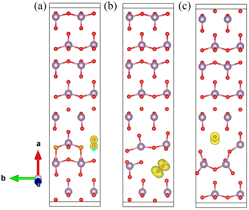
In this work we study the orthorhombic phase of molybdenum trioxide (-MoO3) with the space group symmetry Pnma (62). Lattice parameters of the pristine -MoO3 unit cell after performing geometry optimization were found to be , , [27], and in Fig. 1(a) we show the optimized structure for its supercell.
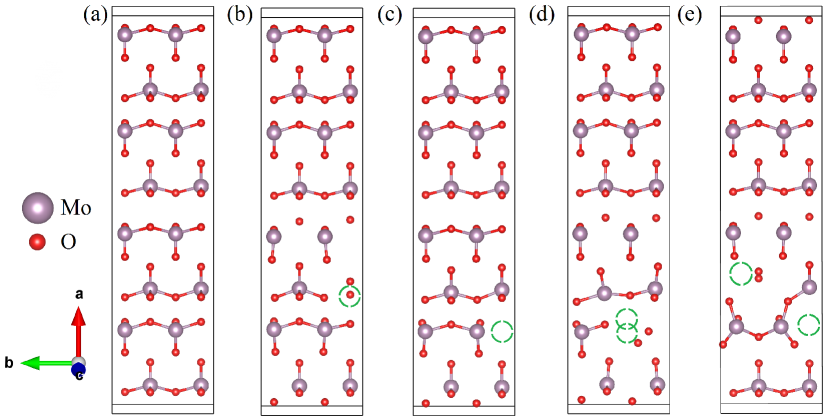
To study the variation of magneto-opto-electronic properties for various types of defects (different types of vacancies) are created in supercell. Figs. 1(b)-1(e) show the optimized supercell structure of -MoO3 with Mo vacancy (VMo), O vacancy (Vo), and Mo-O co-vacancies (VMo+O) of types P1 and P2, respectively.
III.2 Band Structure and Density of States
III.2.1 Pristine Material
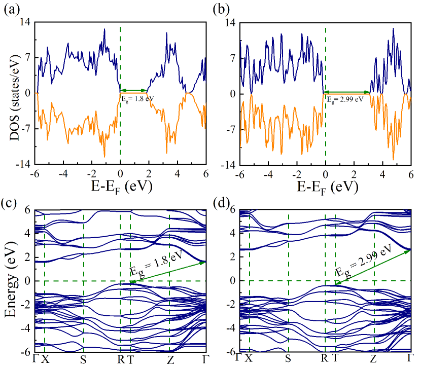
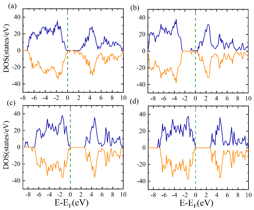
Firstly, we studied the ground-state electronic properties of -MoO3 using spin-polarized DFT simulations. The total density of states (TDOS) and band structure of pristine -MoO3 calculated using the GGA and HSE06 functionals are presented in Figs. 2(a)-2(d). The GGA-level TDOS plot (see Figs. 2(a)) clearly shows symmetry between the up and down spin states indicating non-magnetic behavior, and a finite band gap. As shown in the PBE band structure plot (Fig. 2(c)), we obtain an indirect band gap of 1.8 eV [31]. Along the high-symmetry directions corresponding to -X and R-T, almost degenerate eigenvalues are obtained in the valence and conduction bands. Furthermore, the valence band maxima (VBM) and conduction band minima (CBM) are positioned at T and points, respectively. Our results on the band structure are in good agreement with the previously reported results [31, 62]. In addition, we performed GGA+U calculations to match our band gap with the experimental value. We first applied U correction in the range 2 to 12 eV, only on Mo(4)) electrons. However, the maximum value of the calculated band gap was 2.54 eV for U=9.0 eV, which is still not in good agreement with the experimental value of 3.0-3.3 eV [22, 23, 24]. Given the fact that PDOS (see Fig. 3) analysis reveals that the VBM is entirely composed of O 2 orbitals, thus, next we applied the U correction also to the O(2) electrons, in addition to Mo(4) ones. We found that the choice U (2) = 7 eV for O and eV for Mo does improve the band gap in the sense that it is closer to the experimental value. However, the calculations predict the band gap of the minority spin to be significantly larger than that of the majority spin. Similar behavior is also found in the case i.e., U 9 eV on Mo(4) electrons. This result is in complete contradiction with our GGA and HSE06 results, therefore, we conclude that the DFT+U approach is yielding erroneous results for this system. Therefore, we repeated our calculations using a more accurate hybrid functional, i.e., HSE06, and the results are presented in Figs. 2(b) and 2(d). Indeed, we found an indirect band gap of 2.99 eV using the HSE06 functional, which is in excellent agreement with the experimental value [19]. But, we note that the band structure computed using the HSE06 functional is quite similar to that obtained from GGA, except for the increased band gap.
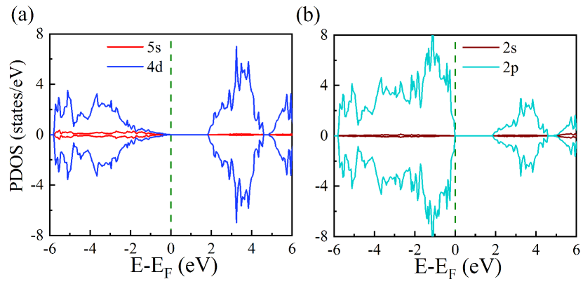
Further, to achieve a better understanding of the contribution of different orbitals in the TDOS, we have calculated the projected density of states (PDOS) of Mo and O atoms, and presented it in Figs. 3(a) and 3(b), respectively. We have computed the PDOS for the 5 and 4 orbitals of the Mo atom, along with the 2 and 2 orbitals of the O atom. From the figure, it is obvious that the majority of the contribution to the TDOS comes from the 4 orbitals of Mo and 2 orbitals of the O atom. Furthermore, the dominant contribution to the TDOS near the Fermi energy is obtained from the 2 orbital of the O atom.
III.2.2 Defective Material
Next, we studied the vacancy-induced electronic properties of -MoO3, and for this purpose, we first created Mo, O, and Mo-O co-vacancies of types P1 and P2 in the supercell, followed by geometry optimization. From the optimized geometry in each case, the band structure, DOS, and optical absorption spectrum were computed. We computed the optical absorption spectra because, experimentally, defect signatures are successfully investigated in oxide samples using optical absorption spectroscopy [63, 34, 33]. Furthermore, DOS can be used for interpreting the experiments, which are performed using transmission electron microscopy [64] and scanning tunneling microscopy [65], thus revealing information on such intrinsic defects in the system. In bulk systems, defect states become very sensitive to the variation in the position of defects in the supercell. The purpose of considering two types of co-vacancies in the supercell is to see whether, or not, the magneto-optoelectronic properties change in the oxides samples with the relative locations of the vacancies.
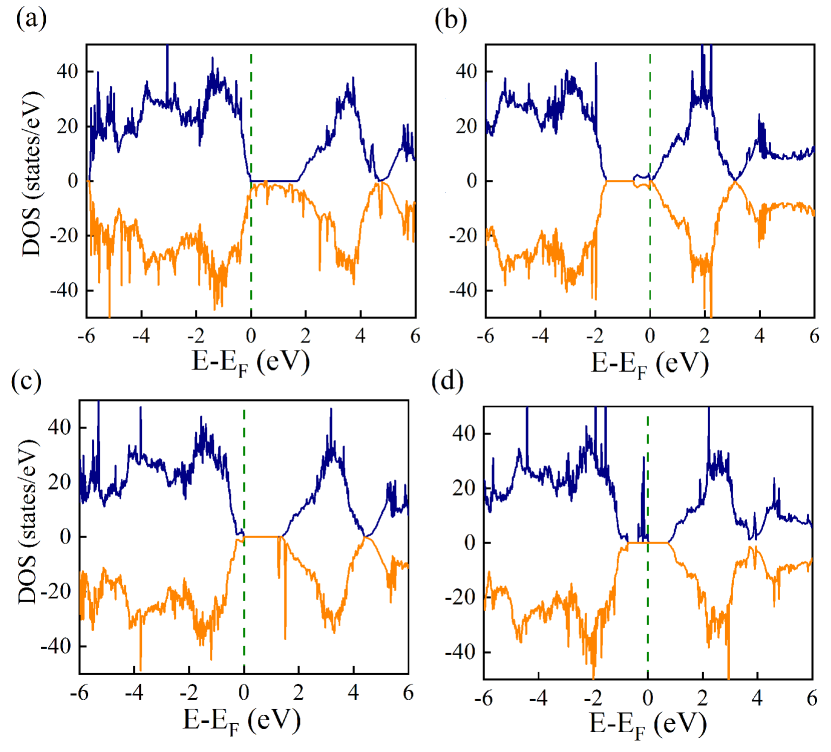
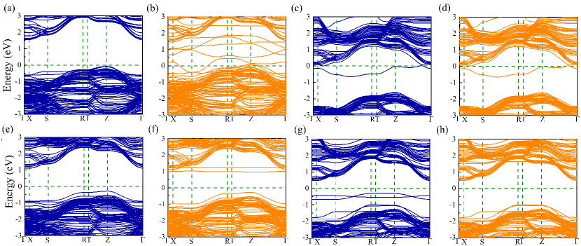
In Figs. 4(a)-4(d), we present the TDOS corresponding to the cases with Mo, O, and Mo-O co-vacancies of types P1 and P2, respectively, using GGA. It is obvious from the figures that the electronic properties of the material change significantly after the introduction of vacancies leading to the appearance of the mid-gap states. With a Mo vacancy (see Fig.4(a)) that corresponds to 6.25 at of vacancy concentration, the system becomes half-metallic with a band gap of 1.63 eV in the majority spin states, while minority spin states show metallic behavior. For the case of O vacancy (see Fig.4(b)) that corresponds to 2.08 at of vacancy concentration, the band gap disappears completely due to the emergence of mid-gap states. Previously, Noby et al. experimentally showed the impact of O vacancy on -MoO3 by considering different oxidizing (oxygen gain) and reducing (oxygen loss) atmospheres [66]. They prepared the samples in different atmospheres (i.e., as prepared, O2-treated, H2-treated, N2-treated and vacuum-treated) and found that the increase in the O vacancies/deficiency led to an increase in electrical conductivity, i.e., a transition from the semi-insulating to the conducting behavior. Chiam et al. investigated the defects-stability in -MoO3 and its role in organic solar cells [67]. They also investigated the presence of mixed oxidation states of Mo (i.e., 4+, 5+ and 6+); as a result of this, they concluded that the defects/vacancies play an important role in the enhancement of device performance. In the case of both types of Mo–O co-vacancies, different band gaps are obtained. A reduced band gap is found in both the P1 and P2 co-vacancies. With the P1 (P2) type of co-vacancy, a band gap of 1.39 (0.78) eV is computed due to the majority spin-states, while minority spin-states show a band gap of 1.23 (1.47) eV. Further, Figs. 5(a)- 5(h) show the band structure for the spin-up and spin-down states corresponding to single Mo, O, and Mo-O co-vacancies of P1 and P2 types in the supercell, respectively. For O vacancy (see Figs. 5(c) and 5(d)), the band structure is identical for the spin-up and spin-down states, which signifies that the system remains non-magnetic in the case of O vacancy. For the Mo vacancy (see Fig. 5(a) and 5(b)), a magnetic moment of 5.98 is obtained, while in the case of Mo-O co-vacancies (see Fig. 5(e)- 5(h) irrespective of their types (i.e., P1 and P2), a magnetic moment of 2.0 is computed.
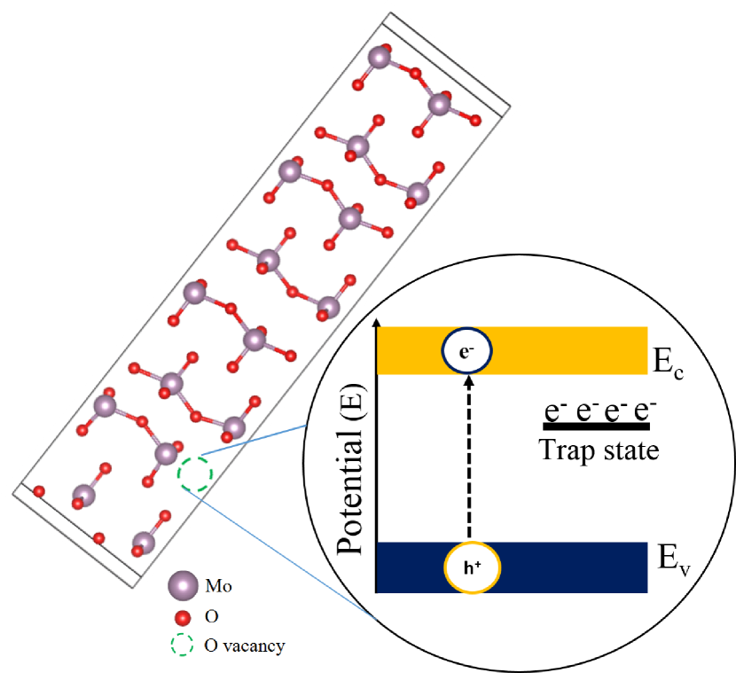
Here, we also highlight the fact that our obtained results are valid for the Mo vacancy concentration of 6.25 at and an O vacancy concentration of 2.08 at. However, in dilute defect limits, the vacancy-induced states, in all likelihood, will be much more localized, as a result of which a single vacancy may not be able to change the transport behaviour of samples from semiconducting to half-metallic/metallic. In Fig. 6, through a schematic, we demonstrate the formation of an O-vacancy-induced mid-gap state between the VBM and CBM, which is nothing but a trap state. The trap states have additional electrons that modify the magneto-optoelectronic properties of the defective system, as compared to the pristine one.
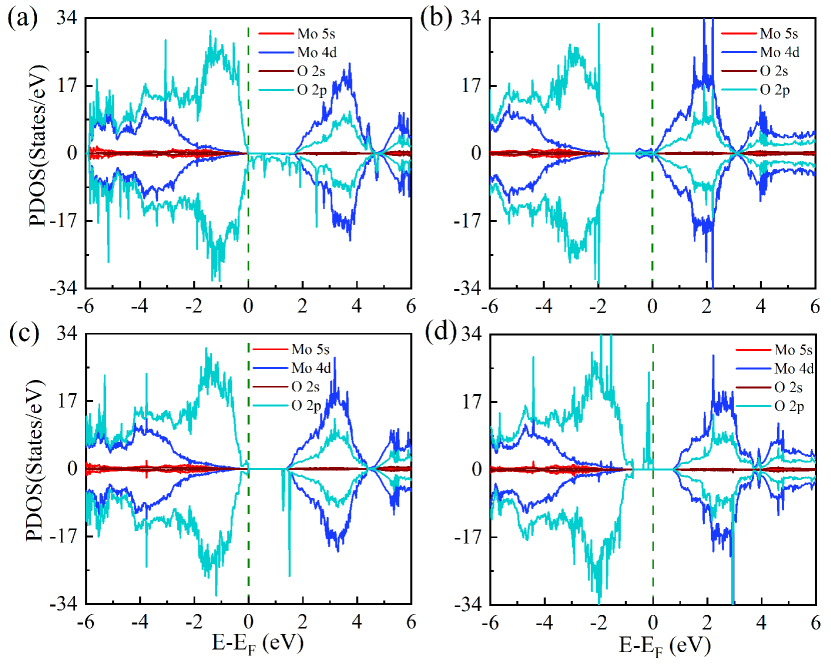
In order to achieve a deeper understanding of the nature of mid-gap states, we computed the PDOS, and our results are presented in Fig. 7. It is clear from the PDOS plot that for the case of Mo vacancy (Fig. 7(a) and Mo-O co-vacancies of both types ((Figs. 7(c) and 7(d)), the contribution to the defect states is more from the O atoms, while for the case of O vacancy (Fig. 7(b), Mo atoms contribute remarkably to the defect states.
Next, we repeated our defect calculations with the hybrid functional, i.e., HSE06, in order to verify our GGA-based results. In the MO-vacancy case (see Fig. 8(a)), our HSE06 calculations reveal the half-metallic nature of the system, as obtained in our GGA results as well. While minority spin states exhibit metallic behavior, the band gap in the majority spin states is computed to be 2.33 eV, which is higher than the GGA computed band gap of 1.63 eV. Moreover, a magnetic moment of 6.0 is obtained that matches well with our GGA computed magnetic moment of 5.98 . In the O vacancy case (see Fig. 8(b)), HSE06 functional predicts the system to be metallic in agreement with our GGA results. Further, the system continues to be non-magnetic; up-spin and down-spin states show symmetrical nature, supporting our GGA findings (see Fig. 4(b)). In P1 and P2 co-vacancies (see Fig. 8(c-d)), semiconducting nature is reported for both, with band gaps of 2.45 eV and 2.66 eV, respectively, which are significantly larger than the corresponding gaps obtained in the GGA calculations. A magnetic moment of 2 is obtained in both types of co-vacancies in HSE06 calculations, in full agreement with the GGA results.
III.3 Spin density analysis
We performed the spin density analysis to understand the contribution of Mo and O atoms to the magnetic moment induced in different vacancy configurations of 221 supercell of -MoO3. Figs. 9(a)- 9(c) show the spin density plots obtained by substracting the up-spin () and down-spin () channels of charge densities correspond to the Mo vacancy and Mo-O co-vacancies of types P1 and P2, for the isovalues of 0.099e, 0.007e, and 0.041e, respectively. As shown in the figures, the spin density isosurface ( shown in yellow color) is mostly concentrated around the O atoms (nearest neighbor atoms of vacancies) in all three cases, which reflects the fact that in all three cases, the contribution from O atoms is more to the magnetic moment. Our spin density plots are qualitatively compatible with the PDOS analysis (see Fig. 7). In addition, the spin density isosurface is dumbbell-shaped, indicating a higher contribution of the orbitals of oxygen to the induced magnetic moments.
III.4 Practical feasibility
We computed the formation energy for (i) Mo vacancy, (ii) O vacancy, and (iii) Mo-O co-vacancies of both types, i.e., P1 and P2, respectively, for the practical realization of the systems with respect to these defect configurations. Before discussing the formation energy of different defect configurations, first, we calculated the formation energy for pristine -MoO3 by considering metallic Mo and O2 gas using the formula
| (6) |
Where is the total energy of the pristine -MoO3 energy per formula unit, and and are the chemical potentials of Mo and O in -MoO3. Moreover, and are the chemical potential of Mo and O in pure molybdenum metal and O2 gas, respectively.
Using Eq. 6, and the obtained values in our DFT simulations, i.e., eV, eV, and eV, we calculated eV, which is in good agreement with the theoretically reported value of -6.77 eV [29] and the experimental value of -7.72 eV [68]. A good matching of formation energy with the previously reported theoretical and experimental results gives us confidence and shows the correctness of our simulation methods.
Next, we calculated the formation energy for the defective systems using Eq. 5, as discussed previously. Using the stability conditions, the following range of chemical potentials for Mo and O have been derived and further used in the formation energy calculation of the defective system
| (7) |
| (8) |
In the above equations, and denote the chemical potentials of Mo and O, in Mo-rich conditions, while and represent those in O-rich conditions. The calculated value of chemical potential in Mo-rich condition for Mo (O) is -10.94 (-7.30) eV, whereas in the O-rich condition it is -18.22 (-4.88) eV. Our computed results of formation energy corresponding to different vacancy configurations are presented in Table 1 (Fig. 10).
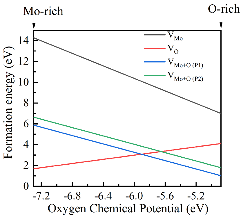
| Vacancy types | VMo | VO | VMo+O(P1) | VMo+O(P2) |
|---|---|---|---|---|
| Mo-rich | 14.28 | 1.69 | 5.58 | 6.65 |
| O-rich | 7.0 | 4.11 | 1.02 | 1.79 |
It is clear from Fig. 10 and Table 1 that the formation energy for Mo vacancy is very high compared to other defect configurations for the entire range of O chemical potential indicating that Mo vacancy is difficult to form at ordinary conditions in -MoO3 [30]. Further, O vacancy in the proximity of VMo (i.e., Mo-O co-vacancies) reduces the formation energy of Mo vacancy considerably. Therefore, our first-principles results indicate that Mo–O co-vacancies support induced magnetic moment in -MoO3, along with reducing the formation energy, and thus stabilizing the Mo vacancy that is responsible for inducing the magnetic moment in the system, as discussed in the previous section. Further, in the Mo-rich condition (i.e., O-poor), O vacancy has the lowest formation energy of 1.69 eV. Further, for the sake of comparison, we note that Cao et al. reported 1.4 eV of formation energy for S vacancy in MoS2 under Mo-rich condition [69], while Kuklin et al. reported 1.64 eV for Se vacancy in PdSe2 under Pd-rich conditions [70]. Our computed value of formation energy for O vacancy is within the usual range of formation energies reported for transition-metal dichalcogenide systems in the literature With the increase in O chemical potential, i.e., towards the O-rich limit, Mo-O co-vacancies of both types start dominating and are more stable compared to the O vacancy. Moreover, the P2 type of Mo-O co-vacancy shows 0.77 eV higher formation energy than P1, implying that the P1 type of co-vacancy is more stable, but on the other hand, both types of co-vacancies exhibit lower formation energy than O vacancy. Here we would like to emphasize the fact that experimentally the stoichiometry of the growth circumstances plays a very crucial role and may affect formation energy values significantly [71].
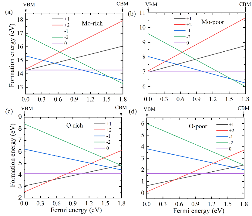
Till now, we discussed the formation energy of neutral vacancies. Next, we considered different charged defect states. We considered +1, +2, -1 and -2 charge states for both Mo and O vacancies and corresponding formation energies are shown in Fig. 11. From the formation energy graphs, it is clear that, as in neutral states, the formation energy of Mo vacancy in different charged states is still high compared with O vacancy. Further, in the O-vacancy case, in both rich and poor conditions, the +1 and +2 states are more stable compared to the negatively charged states, as reported previously [30]. This clearly indicates that the O-vacancy donates electrons to the conduction band to form a stable state. Therefore, O vacancy behaves like a shallow donor, as shown by Noby et al. [66] and is responsible for the unintentional n-type semiconducting behavior of -MoO3.
III.5 Ab-initio MD simulations
In this section, we discuss the results obtained from Ab-initio molecular dynamics (AIMD) simulations, which are performed to investigate the stability and sustainability of the induced magnetic moment, and also to verify the stability of the structure, at room temperature. For technological applications, such as for implementation in spintronic devices, it is important to check not only the structural stability, but also the survival of induced magnetic moments at room temperature. In our study, O vacancy does not induce any kind of magnetic moment in the system, therefore, we performed the AIMD simulations for Mo-O co-vacancy of type P1 owing to the fact that although both types of co-vacancies induce the same magnetic moment (i.e., 2 ), the P1 type of co-vacancy is found to be more stable, as discussed earlier.
Experimentally, to favor the P1 type of Mo-O co-vacancy, one can tune the O chemical potential () within the stability limits as described in Eq. 8 by using the equation
| (9) |
Here, and denote the temperature and pressure of O2, denotes Boltzmann’s constant, and = 1 atm.
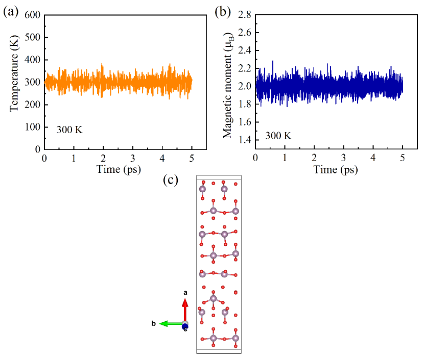
We performed the AIMD simulations for the time period of 5 ps, with the initial temperature fixed at the room temperature taken to be 300 K. Figs. 12(a) and 12(b) show the variation of temperature and magnetic moment as a function of time. In Fig. 12(c), we show the Mo-O co-vacancy structure of P1 type obtained at 300 K. After a time period of 5 ps, we found that the structure remains stable (Fig. 12(c)) with an average magnetic moment of 2 , which exactly matches the obtained value of magnetic moment in our DFT results. The induced magnetic moment is found to be very stable, with minimal variations around 2 , and sustained at the room temperature ( Fig. 12(a)- 12(b)).
III.6 Optical Absorption Spectra
Now, we analyze the optical properties of the system because the optical characteristics of semiconductor oxide materials have generated tremendous research interest due to their potential use in solar cells, photovoltaic materials, etc. In Fig. 13, we present the optical absorption spectra of pristine -MoO3 using the GGA approach. Huang et al. performed a comprehensive first-principles DFT study of the electronic structure and optical properties of pristine and H-doped -MoO3 using the optB88 functional, and reported an optical gap 2.0 eV [25]. Experimentally, Itoh et al. measured the optical gap of the single crystal -MoO3 to be 3.5 eV [72], while in the thin film samples, the corresponding value was found to be 3.1 eV [24, 73, 74]. In our study, we used the convention of Itoh et al. for the a and c axes while plotting the optical absorption spectra [72].
From Fig. 13 it is obvious that the optical gaps (the energy marking the onset of optical absorption) obtained in our PBE functional-based calculations for Ea (Ec) are 2.93 (2.60) eV, which are 0.17 (0.5) eV lower than the thin-film values, and 0.57 (0.9) eV below the single-crystal values. Our DFT computed absorption spectra show considerable anisotropic behavior with respect to the polarization (i.e., Ea vs. Ec), as reported previously in single crystal and thin film-based experiments[72, 24, 73, 74].
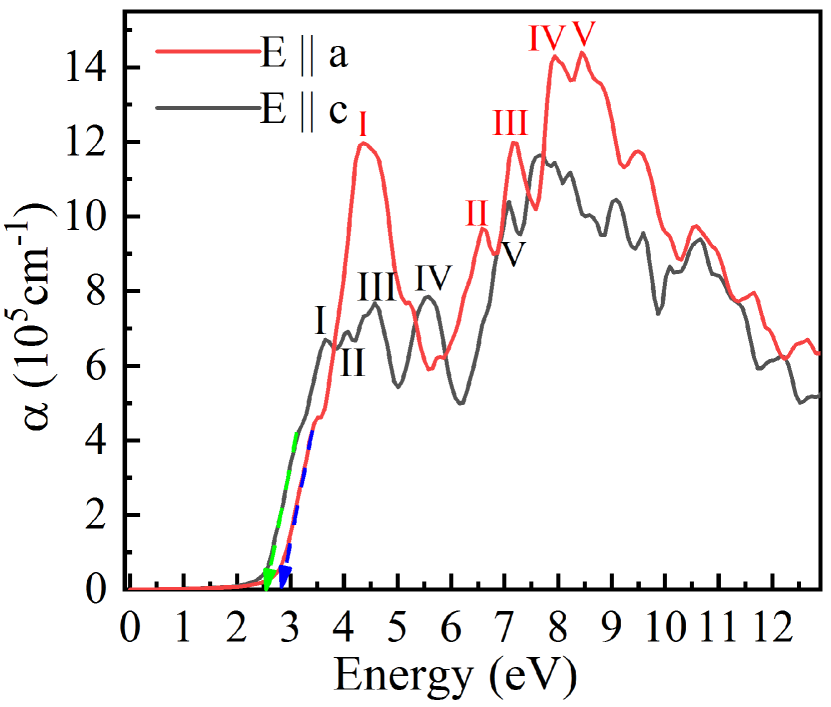
| Peak No. | Peak energy values (eV) | ||
|---|---|---|---|
| Ea | Ec | ||
| I | 4.36 () | 3.64 () | |
| II | 6.58 () | 4.07 () | |
| III | 7.15 () | 4.57 () | |
| IV | 7.94 () | 5.57 () | |
| V | 8.44 () | 7.08 () | |
Moreover, in Ea component of the spectrum, we obtained five different peaks at 4.36 eV, 6.58 eV, 7.22 eV, 7.94 eV, and 8.44 eV. On the other hand, in Ec component, the peaks are at 3.64 eV, 4.07 eV, 4.57 eV, 5.57 eV, and 7.08 eV, respectively. The obtained peak energy values in the absorption spectra for Ea and Ec are shown in Table 2; inside the parentheses, we show the involved Bloch orbitals that contribute to the single-electron transition to that peak value. We found that for the Ea component, all the transitions for five different peak values occur at the point, whereas in Ec, corresponding to the first and the third peak, the transitions are at the T point, while for the rest of the peaks, i.e., the second, fourth, and fifth, the occur at the point. Although, we have not computed the excitonic effects in the absorption spectrum, however, we expect them to be significant, because the exciton binding energy in MoO3 has been estimated to be in the range of 21-28 meV [75, 76]
| Ea (eV) | Ec (eV) | |||||||||
| Peak No. | Mo | O | Mo-O co- | Mo-O co- | Mo | O | Mo-O co- | Mo-O co- | ||
| vacancy | vacancy | vacancy (P1) | vacancy (P2) | vacancy | vacancy | vacancy (P1) | vacancy (P2) | |||
| I | 4.36 | 4.37 | 4.35 | 4.33 | 3.63 | 3.71 | 3.59 | 3.62 | ||
| II | 6.58 | 6.59 | 6.64 | 6.57 | 4.45 | 4.32 | 4.35 | 4.09 | ||
| III | 7.17 | 7.20 | 7.19 | 7.24 | 5.54 | 5.59 | 5.55 | 5.52 | ||
| IV | 7.63 | 7.92 | 7.62 | 7.67 | 6.69 | 6.98 | 6.97 | 6.95 | ||
| V | 8.26 | 8.47 | 8.28 | 8.29 | 7.94 | 7.64 | 7.95 | 7.95 | ||
Next, we analyze the optical properties of defective systems of 221 supercell of -MoO3. Figs. 14(a)- 14(d) show the absorption spectra of the supercell with Mo-vacancy, O-vacancy, and Mo-O co-vacancies of types P1 ad P2, respectively. It is obvious from the plots that due to the introduction of vacancies into the system, some new peaks have emerged in the absorption spectra below the main band edge. In the Mo vacancy case (Fig. 14(a)), below the band edge, two peaks are obtained at 0.47 eV (c1) and 1.23 eV (c2) for the Ea component, and 0.33 eV (a1) and 2.0 eV (a2) in the Ec component
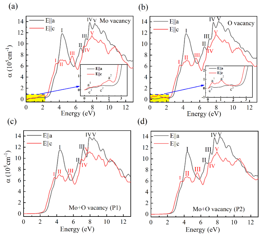
(see inset of Fig. 14(a)). In case of the O vacancy (Fig. 14(b)), the peak positions below the band edge are obtained at 0.27 eV (c1) and 1.86 eV (c2) for Ea, and 0.36 eV (a1) and 1.04 eV (a2) for Ec (see inset of Fig. 14(b)), respectively. Interestingly, there are no peaks obtained below the band edge in the Mo-O co-vacancies of both types. As in the case of the pristine system, for the defective systems also we obtain five different absorption peaks in the absorption spectra corresponding to the Mo, O, and Mo-O co-vacancies ( Fig. 14(a)-14(d)). The calculated peak energy values for different defect configurations are presented in Table 3.
IV Conclusion
In this work we presented a first-principles DFT-based systematic study of electronic, optical, and magnetic properties of crystalline -MoO3 both in its pristine form and with various vacancy configurations. Due to the vacancies, mid-gap states appear, modifying the properties of the system significantly. From the formation energy calculations, we conclude that O vacancies (in the Mo-rich limit) and Mo-O co-vacancies (in the O-rich limit) are more favorable defects in the -MoO3, compared with the Mo vacancies in the system. Although, the pristine -MoO3 is a non-magnetic semiconductor, however, our calculations predict that configurations with Mo vacancy and Mo-O co-vacancies give rise to a finite magnetic moment in the system. Mo vacancy leads not only to a very large magnetic moment of 5.98 , but also gives rise to half-metallicity in the system, which can be useful in spintronic applications. In the case of Mo-O co-vacancies, a comparatively lower but still significant magnetic moment of 2.0 is induced in the system, indicating the possibility of the realization of magnetic behavior in the material by defect engineering. In the optical absorption spectra of configurations Mo/O vacancies, we observe peaks in the gap region, however, these peaks vanish for configurations with Mo-O co-vacancies just like in the pristine state of -MoO3. This suggests that optical absorption spectroscopy can be used for defect identification in the system.
V Acknowledgement
P S acknowledges UGC, India, for the senior research fellowship [Grant No. 1330/(CSIR-UGC NET JUNE 2018)]. All the calculation results were obtained using the computational facilities (Spacetime cluster) of the Department of Physics, IIT Bombay.
References
- Wei et al. [2009] G. Wei, W. Qin, D. Zhang, G. Wang, R. Kim, K. Zheng, and L. Wang, Journal of Alloys and Compounds 481, 417 (2009).
- Chernova et al. [2009] N. A. Chernova, M. Roppolo, A. C. Dillon, and M. S. Whittingham, Journal of Materials Chemistry 19, 2526 (2009).
- Saji and Lee [2012] V. S. Saji and C.-W. Lee, ChemSusChem 5, 1146 (2012).
- Lee et al. [2008] S.-H. Lee, Y.-H. Kim, R. Deshpande, P. A. Parilla, E. Whitney, D. T. Gillaspie, K. M. Jones, A. H. Mahan, S. Zhang, and A. C. Dillon, Advanced Materials 20, 3627 (2008).
- You et al. [2007] H. You, Y. Dai, Z. Zhang, and D. Ma, Journal of Applied Physics 101, 026105 (2007).
- Meyer et al. [2012] J. Meyer, S. Hamwi, M. Kröger, W. Kowalsky, T. Riedl, and A. Kahn, Advanced materials 24, 5408 (2012).
- Bao et al. [2010] Q. Bao, J. Yang, Y. Li, and J. Tang, Applied physics letters 97, 172 (2010).
- De Castro et al. [2017] I. A. De Castro, R. S. Datta, J. Z. Ou, A. Castellanos-Gomez, S. Sriram, T. Daeneke, and K. Kalantar-zadeh, Advanced Materials 29, 1701619 (2017).
- Lin et al. [2010] S.-Y. Lin, C.-M. Wang, K.-S. Kao, Y.-C. Chen, and C.-C. Liu, Journal of sol-gel science and technology 53, 51 (2010).
- Xiang et al. [2014] D. Xiang, C. Han, J. Zhang, and W. Chen, Scientific reports 4, 1 (2014).
- Balendhran et al. [2013a] S. Balendhran, J. Deng, J. Z. Ou, S. Walia, J. Scott, J. Tang, K. L. Wang, M. R. Field, S. Russo, S. Zhuiykov, et al., Advanced Materials 25, 109 (2013a).
- Balendhran et al. [2013b] S. Balendhran, S. Walia, M. Alsaif, E. P. Nguyen, J. Z. Ou, S. Zhuiykov, S. Sriram, M. Bhaskaran, and K. Kalantar-Zadeh, ACS nano 7, 9753 (2013b).
- Ji et al. [2016] F. Ji, X. Ren, X. Zheng, Y. Liu, L. Pang, J. Jiang, and S. F. Liu, Nanoscale 8, 8696 (2016).
- Rahman et al. [2018] F. Rahman, T. Ahmed, S. Walia, E. Mayes, S. Sriram, M. Bhaskaran, and S. Balendhran, Nanoscale 10, 19711 (2018).
- Hanlon et al. [2014] D. Hanlon, C. Backes, T. M. Higgins, M. Hughes, A. O’Neill, P. King, N. McEvoy, G. S. Duesberg, B. Mendoza Sanchez, H. Pettersson, et al., Chemistry of Materials 26, 1751 (2014).
- Gao et al. [2012] B. Gao, H. Fan, and X. Zhang, Journal of Physics and Chemistry of Solids 73, 423 (2012).
- Boudaoud et al. [2006] L. Boudaoud, N. Benramdane, R. Desfeux, B. Khelifa, and C. Mathieu, Catalysis today 113, 230 (2006).
- Chithambararaj and Bose [2011] A. Chithambararaj and A. C. Bose, Journal of Alloys and Compounds 509, 8105 (2011).
- Sinaim et al. [2012] H. Sinaim, D. J. Ham, J. S. Lee, A. Phuruangrat, S. Thongtem, and T. Thongtem, Journal of alloys and compounds 516, 172 (2012).
- Sreedhara et al. [2013] M. Sreedhara, H. R. Matte, A. Govindaraj, and C. Rao, Chemistry–An Asian Journal 8, 2430 (2013).
- Patzke et al. [2004] G. R. Patzke, A. Michailovski, F. Krumeich, R. Nesper, J.-D. Grunwaldt, and A. Baiker, Chemistry of materials 16, 1126 (2004).
- Chen et al. [2010] Y. Chen, C. Lu, L. Xu, Y. Ma, W. Hou, and J.-J. Zhu, CrystEngComm 12, 3740 (2010).
- Hu et al. [2009] B. Hu, L. Mai, W. Chen, and F. Yang, Acs Nano 3, 478 (2009).
- Carcia and McCarron Iii [1987] P. Carcia and E. McCarron Iii, Thin Solid Films 155, 53 (1987).
- Huang et al. [2014] P.-R. Huang, Y. He, C. Cao, and Z.-H. Lu, Scientific reports 4, 1 (2014).
- Li and Chen [2013] F. Li and Z. Chen, Nanoscale 5, 5321 (2013).
- Akande et al. [2016] S. O. Akande, A. Chroneos, M. Vasilopoulou, S. Kennou, and U. Schwingenschlögl, Journal of Materials Chemistry C 4, 9526 (2016).
- Inzani et al. [2016] K. Inzani, T. Grande, F. Vullum-Bruer, and S. M. Selbach, The Journal of Physical Chemistry C 120, 8959 (2016).
- Das et al. [2019] T. Das, S. Tosoni, and G. Pacchioni, Computational Materials Science 163, 230 (2019).
- Peelaers et al. [2017] H. Peelaers, M. Chabinyc, and C. Van de Walle, Chemistry of Materials 29, 2563 (2017).
- Qu et al. [2017] Q. Qu, W.-B. Zhang, K. Huang, and H.-M. Chen, Computational Materials Science 130, 242 (2017).
- Bandaru et al. [2018] S. Bandaru, G. Saranya, N. J. English, C. Yam, and M. Chen, Scientific reports 8, 1 (2018).
- Mishra et al. [2019] V. Mishra, M. K. Warshi, A. Sati, A. Kumar, V. Mishra, R. Kumar, and P. Sagdeo, SN Applied Sciences 1, 1 (2019).
- Mishra et al. [2018] V. Mishra, M. K. Warshi, A. Sati, A. Kumar, V. Mishra, A. Sagdeo, R. Kumar, and P. R. Sagdeo, Materials Science in Semiconductor Processing 86, 151 (2018).
- Jupille and Thornton [2015] J. Jupille and G. Thornton, Defects at oxide surfaces, Vol. 58 (Springer, 2015).
- Kan et al. [2005] D. Kan, T. Terashima, R. Kanda, A. Masuno, K. Tanaka, S. Chu, H. Kan, A. Ishizumi, Y. Kanemitsu, Y. Shimakawa, et al., Nature materials 4, 816 (2005).
- Wu et al. [2010] Z. Wu, M. Li, J. Howe, H. M. Meyer III, and S. H. Overbury, Langmuir 26, 16595 (2010).
- Courths et al. [1989] R. Courths, B. Cord, and H. Saalfeld, Solid state communications 70, 1047 (1989).
- Goes et al. [2018] W. Goes, Y. Wimmer, A.-M. El-Sayed, G. Rzepa, M. Jech, A. L. Shluger, and T. Grasser, Microelectronics Reliability 87, 286 (2018).
- Deák et al. [2019] P. Deák, M. Lorke, B. Aradi, and T. Frauenheim, Journal of Applied Physics 126, 130901 (2019).
- Freysoldt et al. [2014] C. Freysoldt, B. Grabowski, T. Hickel, J. Neugebauer, G. Kresse, A. Janotti, and C. G. Van de Walle, Reviews of modern physics 86, 253 (2014).
- Kohan et al. [2000] A. Kohan, G. Ceder, D. Morgan, and C. G. Van de Walle, Physical Review B 61, 15019 (2000).
- Zheng et al. [2006] J. Zheng, G. Ceder, T. Maxisch, W. K. Chim, and W. K. Choi, Physical Review B 73, 104101 (2006).
- Venkatesan et al. [2004] M. Venkatesan, C. B. Fitzgerald, and J. M. D. Coey, Nature 430, 630 (2004).
- Pemmaraju and Sanvito [2005] C. D. Pemmaraju and S. Sanvito, Physical review letters 94, 217205 (2005).
- Elfimov et al. [2002] I. Elfimov, S. Yunoki, and G. Sawatzky, Physical review letters 89, 216403 (2002).
- Rahman et al. [2008] G. Rahman, V. M. García-Suárez, and S. C. Hong, Physical Review B 78, 184404 (2008).
- Rahman et al. [2013] G. Rahman, N. U. Din, V. M. Garcia-Suarez, and E. Kan, Physical Review B 87, 205205 (2013).
- Khalid et al. [2009] M. Khalid, M. Ziese, A. Setzer, P. Esquinazi, M. Lorenz, H. Hochmuth, M. Grundmann, D. Spemann, T. Butz, G. Brauer, et al., Physical Review B 80, 035331 (2009).
- Pandey et al. [2022] S. Pandey, A. Shukla, and A. Tripathi, Computational Materials Science 210, 111037 (2022).
- Wang et al. [2016] Q. Wang, M. Brier, S. Joshi, A. Puntambekar, and V. Chakrapani, Physical Review B 94, 245305 (2016).
- Guo and Robertson [2014] Y. Guo and J. Robertson, Applied Physics Letters 105, 222110 (2014).
- Lambert et al. [2017] D. Lambert, S. Murphy, A. Lennon, and P. Burr, RSC advances 7, 53810 (2017).
- Kresse and Furthmüller [1996a] G. Kresse and J. Furthmüller, Physical review B 54, 11169 (1996a).
- Kresse and Furthmüller [1996b] G. Kresse and J. Furthmüller, Computational materials science 6, 15 (1996b).
- Mortensen et al. [2005] J. J. Mortensen, L. B. Hansen, and K. W. Jacobsen, Physical Review B 71, 035109 (2005).
- Kresse and Joubert [1999] G. Kresse and D. Joubert, Physical review b 59, 1758 (1999).
- Perdew et al. [1996] J. P. Perdew, K. Burke, and M. Ernzerhof, Physical review letters 77, 3865 (1996).
- Monkhorst and Pack [1976] H. J. Monkhorst and J. D. Pack, Physical review B 13, 5188 (1976).
- Ehrenreich and Cohen [1959] H. Ehrenreich and M. H. Cohen, Physical Review 115, 786 (1959).
- Ravindran et al. [1999] P. Ravindran, A. Delin, B. Johansson, O. Eriksson, and J. Wills, Physical Review B 59, 1776 (1999).
- Dandogbessi and Akin-Ojo [2016] B. S. Dandogbessi and O. Akin-Ojo, Journal of Applied Physics 120, 055105 (2016).
- Du et al. [2010] A. Du, Z. Zhu, and S. C. Smith, Journal of the American Chemical Society 132, 2876 (2010).
- Hashimoto et al. [2004] A. Hashimoto, K. Suenaga, A. Gloter, K. Urita, and S. Iijima, nature 430, 870 (2004).
- Ugeda et al. [2010] M. M. Ugeda, I. Brihuega, F. Guinea, and J. M. Gómez-Rodríguez, Physical Review Letters 104, 096804 (2010).
- Noby et al. [2022] S. Z. Noby, A. Fakharuddin, S. Schupp, M. Sultan, M. Krumova, M. Drescher, M. Azarkh, K. Boldt, and L. Schmidt-Mende, Materials Advances 3, 3571 (2022).
- Chiam et al. [2012] S. Chiam, B. Dasgupta, D. Soler, M. Leung, H. Liu, Z. Ooi, L. Wong, C. Jiang, K. Chang, and J. Zhang, Solar energy materials and solar cells 99, 197 (2012).
- Speight [2005] J. G. Speight, Lange’s Handbook of Chemistry, 16th ed.; McGraw-Hill: New York, NY, USA , 1 (2005).
- Cao et al. [2016] D. Cao, H. Shu, T. Wu, Z. Jiang, Z. Jiao, M. Cai, and W. Hu, Applied Surface Science 361, 199 (2016).
- Kuklin et al. [2021] A. V. Kuklin, L. V. Begunovich, L. Gao, H. Zhang, and H. Ågren, Physical Review B 104, 134109 (2021).
- Koós et al. [2019] A. A. Koós, P. Vancsó, M. Szendrő, G. Dobrik, D. Antognini Silva, Z. I. Popov, P. B. Sorokin, L. Henrard, C. Hwang, L. P. Biró, and L. Tapasztó, The Journal of Physical Chemistry C 123, 24855 (2019).
- Itoh et al. [2001] M. Itoh, K. Hayakawa, and S. Oishi, Journal of Physics: Condensed Matter 13, 6853 (2001).
- Sabhapathi et al. [1994] V. Sabhapathi, O. M. Hussain, S. Uthanna, and P. J. Reddy, Materials Letters 20, 175 (1994).
- Sabhapathi et al. [1995] V. Sabhapathi, O. M. Hussain, S. Uthanna, B. S. Naidu, and P. J. Reddy, Journal of materials science letters 14, 411 (1995).
- Shahrokhi et al. [2020] M. Shahrokhi, P. Raybaud, and T. Le Bahers, Journal of Materials Chemistry C 8, 9064 (2020).
- Fogle and Perlstein [1972] W. Fogle and J. H. Perlstein, Physical Review B 6, 1402 (1972).