![[Uncaptioned image]](/html/2306.04493/assets/x2.png)
![]()
|
|
Manipulation of the electrical and memory properties of MoS2 field-effect transistors by highly charged ion irradiation† |
| Stephan Sleziona,∗a Aniello Pelella,b Enver Faella,b Osamah Kharsah,a Lucia Skopinski,a Andre Maas,a Yossarian Liebsch,a Antonio Di Bartolomeo,b and Marika Schlebergera | |
|
|
Field-effect transistors based on molybdenum disulfide () exhibit a hysteresis in their transfer characteristics, which can be utilized to realize 2D memory devices. This hysteresis has been attributed to charge trapping due to adsorbates, or defects either in the lattice or in the underlying substrate. Wefabricated MoS2 field-effect transistors on /Si substrates, irradiated these devices with ions at a kinetic energy of 180 keV to deliberately introduce defects and studied the resulting changes of their electrical and hysteretic properties. We find clear influences of the irradiation: While the charge carrier mobility decreases linearly with increasing ion fluence (up to only 20 % of its initial value) the conductivity actually increases again after an initial drop of around two orders of magnitude, likely due to the occurence of hopping transport via localized states. We also find a significantly reduced -doping ( cm-2) and a well-developed hysteresis after the irradiation. The hysteresis height increases with increasing ion fluence and enables us to characterize the irradiated field-effect transistor as a memory device with remarkably longer relaxation times ( minutes) compared to previous works. |
1 Introduction
Molybdenum disulfide (), a member of the family of the so-called transition metal dichalcogenides (TMDCs), is one of the most studied two-dimensional (2D) materials right after graphene. While in its bulk (3D) form it has an indirect bandgap of around 1.2 eV1, it develops a direct bandgap of 1.8-1.9 eV2 when reduced to its covalently bonded S-Mo-S monolayer structure. This bandgap allows the utilization of as typical building blocks for modern electronics like e.g., field-effect transistors (FETs) based on atomically thin 2D materials 3. Because of that, it was quickly realized that monolayer might be an excellent candidate for future electronic and opto-electronic applications, especially when large scale production techniques such as chemical vapor deposition (CVD) are used. The on-going reduction of device dimensions poses critical problems for traditional semiconductor devices e.g. based on silicon, as the carrier mobility degrades rapidly for channel thicknesses reaching the scale of only a few nm 4, 5, 6, which is not the case for and other 2D materials 7. Indeed it was demonstrated that FETs with a small gate length ( 10 nm) and simultaneously reasonable mobility and high on-currents can be achieved 8, 9. Open challenges for 2D-TMDC FETs to date are Schottky barriers at the metal-TMDC interface 10, 11, non-sufficient doping techniques 12 and structural defects either in the channel material or in the underlying oxide 13. These structural defects can trap charges and act as scattering centres, modifying the electrical properties of the devices. One prominent consequence of these defects is the occurrence of a hysteresis in the transfer characteristics ()) of a FET, which is commonly observed for (and other TMDC) based devices 14, 15, 16, 17, 18. The trapped charges influence the charge carriers in the 2D material channel and shift the transfer characteristics depending on the gate voltage sweep direction. Although most of the time the hysteresis should be prevented or eliminated for stable device performance, it can also be exploited to achieve atomically thin memory devices 19, 20, 21, 15.
Defects can be artificially and controllably introduced into 2D materials by particle irradiation, e.g. using electrons or ions as projectiles. While electron irradiation often leads to the creation of single vacancies 22, 23, ion irradiation can additionally cause more complex defects, depending on the ion type and energy 24, 25, 26, 27. These defects have been proposed or even utilized for a broad variety of applications, e.g. ultrafiltration 28, 29, DNA sequencing 30, 31 or catalysis 32. By fine tuning the energy of the ions, irradiation can even be used to clean the surface of 2D materials from process residues stemming from transfer and lithography steps, without damaging the underlying 2D material too much 33, 34. Although there has been done some work with particle irradiation of 2D FETs 35, 36, 37, 38 these works focus mostly only on standard electrical performance like conductivity, mobility and their irradiation hardness 39, 40, 41 and not on manipulating the hysteretic properties of the irradiated devices.
With this work we want to close this gap and additionally pay specific attention to the manipulation of the hysteretic properties of 2D FETs by ion irradiation. To this end we fabricate CVD-grown single layer FETs on a substrate via photolithography and characterize their electrical properties by measuring their output and transfer characteristics. After this initial characterization, the devices are irradiated with highly charged ions (HCI) to deliberately introduce defects. We use HCIs as projectiles since their potential energy (e.g. their charge state) and kinetic energy can be tuned independently and by that control the defect creation in our devices. In this work we have chosen a relatively high kinetic energy so that we also expect defect creation in the substrate (see 42 for details). We show that the irradiation leads to distinct modifications of the electrical properties and especially causes a strongly reduced n-doping of the devices. Most importantly, we demonstrate that the irradiation leads to the opening of a hysteresis, most likely caused by additional defects in the underlying oxide. The height of the hysteresis scales with the introduced ion fluence, enabling the realisation of a memory device.
2 Results and discussion
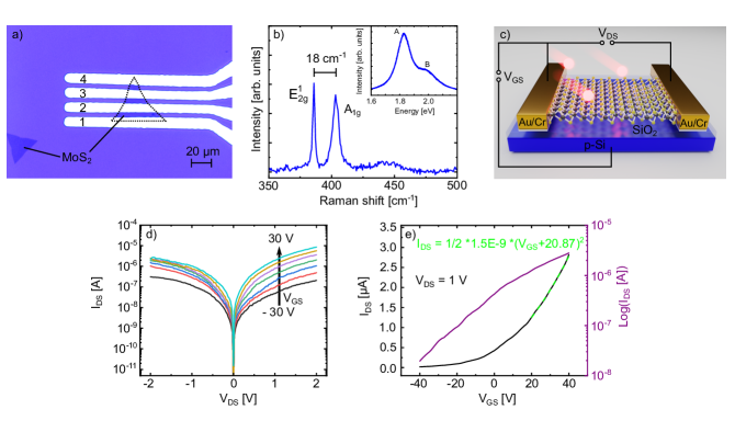
We begin by describing our devices and the general course of our work. In Fig. 1 a) an optical microscopy image of one of the -FETs used in this work is shown. The four metal contacts are labeled with numbers (1-4). For most devices, we employed a two-point measurement configuration where two contacts right next to each other were used as drain and source contact. For example, for the device shown in the image, the contacts 1 and 2 were used. Fig. 1 b) shows typical Raman and Photoluminescence (PL) data for our FETs after their fabrication. The two well-known Raman modes and are present and the difference in their positions in the spectrum is . The inset shows the PL spectrum measured at the same spatial position, displaying one strong peak at an energy of 1.83 eV attributed to the A exciton and a smaller peak at an energy of 1.98 eV attributed to the B exciton. Both observations clearly proof that our samples are indeed monolayers of 43, 2. Fig. 1 c) outlines the general course of our experiment: The FET structure is used for standard electrical characterization of the , in particular the output (()) and transfer (()) characteristics. After this initial characterization, the devices are irradiated with highly charged ions at a kinetic energy of 180 keV to deliberately introduce defects into the devices. Afterwards, the devices are again characterized to observe the influence of the introduced defects on their electrical behavior. We irradiated four different devices with four different fluences, namely 100 ions/m2, 200 ions/m2, 400 ions/m2 and 1600 ions/m2.
The output and transfer characteristics of one of our device before the irradiation is shown exemplary in Figure 1 d) and e), respectively. The output characteristics displays a slightly rectifying Schottky barrier between the channel and the contacts, which is a common observation for -FETs, since mid-gap Fermi level pinning arises from defects at various metal-TMDC interfaces caused e.g. by the processing conditions 44, 45, 46, 47, 48, 49. The transfer characteristics in Figure 1 e) reveals the behavior of a normally-on n-type transistor with very strong n-doping. is typically found to be n-doped, which is attributed to electron-donating sulfur vacancies 50, 51, 52, 53. Consequently, the off-state of the transistor can not be reached in the applied gate voltage range, so the ratio between the minimum and maximum current is only . We note that the devices in this work exhibit small differences in their overall electrical behavior, which is a typical observation for 2D devices in literature and can be explained by the contact resistance and Fermi-level pinning being delicately dependent on microscopic details in the contact formation at the metal-TMDC interface 54, 47. Nevertheless, all our devices have in common that they have a low Schottky barrier and exhibit strong n-doping.

In Figure 2 a) and b) the output and transfer characteristics of the device before (blue) and after irradiation (red) with a fluence of 400 ions/m2 are shown. Let us discuss the output characteristic in Fig. 2 (a) first. It displays a reduction of the current by around two orders of magnitude after the irradiation. Besides that, the Schottky type behavior is not modified. This finding is within our expectations: Particle irradiation of contacts can modify the metal-2D material interface in such devices and lead to reduced contact resistance and Schottky barriers 55, 56. In our work however, the kinetic energy of the ions is not high enough to penetrate through the metal contacts, as supported by SRIM calculations that demonstrate that all ion collision events occur only in the metal and not at the interface (see Figure S1 a)). This means that all the energy of the ions is deposited into the metal and not at the metal-TMDC interface from which follows, that the interface can not be modified by the irradiation.
The strong reduction of indicates a significant increase in scattering centers. The irradiation of the itself with electrons or ions with a moderate kinetic energy ( keV) can lead to single or double vacancy defects in the TMDC lattice 57, 58, 59. In contrast, the defect creation mechanism by HCIs in 2D materials is still under discussion 60. For free-standing , the formation of nm-sized holes after HCI irradiation was observed, where the size of the holes depends on the charge state of the ions 61. Unfortunately to the best of our knowledge, there are no corresponding imaging experiments for substrate-supported monolayers to date. However, recent time-of-flight mass spectrometry experiments show that the kinetic energy of the HCIs additionally has to be taken into account for substrate supported MoS2 and that the HCI-MoS2 interaction is also dependent on the type of the substrate 42.
Molecular dynamics simulations for substrate-supported irradiated with cluster ions suggest, that there are also holes created in the lattice, which have a bigger diameter than in the free-standing case 62. Additionally, the substrate also gets modified, exhibiting, e.g., hillocks and thereby induce strain in the surrounding 2D material. Regardless of the specific defect type created by the irradiation (vacancies, holes, strained/chemically modified lattice), all of them will pose scattering centres for the charge carriers and thus reduce the conductivity of our device.
We will now discuss the transfer characteristics in Figure 2 b) which shows striking differences between the measurement before (blue) and after (red) the irradiation. As discussed for Figure 1 e), the transfer characteristics before the irradiation displays a strong n-doping behavior. When sweeping the gate voltage between -30 V and +30 V and back, no hysteresis effect is observed. This might be caused by the strong n-doping of our devices, since the saturation region of the transfer characteristics usually does not show a significant hysteretic behavior when measured in high vacuum conditions 14, 16, 21. After the irradiation, the most striking difference is the appearance of the off-state region and a hysteresis in the transfer characteristics. As mentioned before, this hysteresis is generally attributed to either defects in the lattice, at the /oxide interface or in the oxide itself 21, 16, 63. As the occurrence of the hysteresis is clearly related to the irradiation it seems straightforward to claim that it is a result of additional defects introduced by the irradiation. The right-shift of the transfer after the forward gate voltage sweep, which leads to the clockwise hysteresis, is indicative of negative charge trapping. A further discussion of the properties of the hysteresis and which type of defect is likely the reason for its occurrence will be conducted later on. Additionally, the transfer curve shows, that the n-doping of the device is strongly reduced after the irradiation, since the threshold voltage () shifts towards positive gate voltages. It is now even possible to reach the off-state of the transistor in the applied gate voltage range and a high on-off ratio of nearly 6 orders of magnitude can be derived.
This reduction of n-type doping may be attributed to several possible causes. Oxygen molecules capture electrons in 64, 65, 66 and at the dangling bonds of the 2D material defect sites, the chemical and physical adsorption of molecules can be enhanced 67, 68, 69. Although the amount of adsorbed molecules should be reduced under vacuum conditions, ion irradiation can even lead to the formation of chemically adsorbed at the defect edges, which would be very resistant to vacuum assisted desorption 32 and could also explain the observed reduction in n-doping. Since the HCIs will not only deposit their energy in the monolayer, but also in the underlying substrate, defects in the oxide could also play a role in p-doping the device. In fact, electron-trapping defect states for on a substrate have already been reported 63, 70, 71 and would lead to an effective p-doping of our devices by an additional gating effect. The trapped negative charges in the oxide influence the electric field generated by the applied gate voltage and thereby shifting the transfer curve towards positive gate voltages.
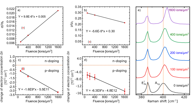
In the following, we will compare the results of the electrical characterization before and after the irradiation of our devices in dependence of the irradiation fluence. For this, we will address the conductivity, mobility, and charge carrier density, starting with the conductivity. In Figure 3 a) we display the remaining conductivity () using the output characteristics before and after irradiation. That is, we normalized the conductivity after irradiation to its value before irradiation to compare the different devices with each other. Interestingly, the devices show an increasing remaining conductivity with increasing ion fluence, after the initial drop in conductivity already discussed above (see Figure 2 a)). This peculiar behavior could be connected to an irradiation induced activation of an additional transport mechanism. For 2D TMDCs it has already been shown, that an increase in chalcogen vacancies or interface defects can lead to hopping transport via localized states and, as a consequence, lead to an increasing conductivity 50, 72. Note, that the FET irradiated with 200 ions/m2 is the only exception to the otherwise linear behavior. For this device we used the contacts 1 and 3 as source and drain contact with one contact (2) in between on the channel (see Figure 1 a)). By Fermi-level pinning this contact can modify the electrical behavior of the 2D material channel, which is mirrored in all electrical characterizations (Figure 3 a)-c)). We have therefore excluded this data point from our discussion.
Next, we calculate the effective mobility by fitting the equation to the transfer characteristics at high gate voltages ( 20 V). With ) and = F/cm2 we obtain values between 0.5-10 cm2/Vs for the devices used in this work, which is in the range typically measured for such devices 73, 14, 74. After the irradiation, the mobility was examined again and then normalized to the value measured before the irradiation (). The results of this analysis are shown in Figure 3 b) displaying a monotonous decrease of the mobility with increasing ion fluence. The defects introduced by the HCI irradiation either in the or in the oxide can lead to increased Coulomb scattering for the charge carriers in our devices by charge trapping. This leads to shorter scattering times and therefore an overall reduced mobility, despite the enhanced remaining conductivity.
Lastly, we discuss the change in charge carrier density. We quantitatively evaluate the change in doping for our devices using the transfer characteristics of each device before and after irradiation. Because of the initially high n-doping of our devices we use to fit the transfer curve and extract the value for (see green-streaked line in Figure 1 e))16. From this we calculated the change in charge carrier concentration with . As can be seen in Figure 3 c) , the irradiation leads to less n-doping (i.e. effective p-doping) in our devices in the order of cm-2 and increases with increasing ion fluence up to 3.0 cm-2 without any indication of a saturation behavior.
To further confirm this finding, we performed Raman spectroscopy of a CVD-grown sample between the different irradiation steps (see Figure 3 e)). The qualitative behavior of the Raman spectra, a constant position for the mode, while the mode shifts to higher wavenumbers, points to decreasing n-doping 75, as it was also derived from the transfer characteristics. We also find a stronger reduction of the n-doping with increasing ion fluence. For a quantitative analysis we used the procedure from ref. 76. The result of this is shown in Figure 3 d). Obviously, both methods, electrical characterization and evaluation of Raman spectra, yield the same result, a linearly decreasing n-doping with increasing irradiation fluence, supporting our previous findings. The absolute values extracted from the Raman data are somewhat higher than those extracted from the transfer characteristics which can be explained by the fact that the Raman spectra were collected in ambient conditions, while the FETs were measured under high vacuum conditions. Therefore, the reduction of n-doping in MoS2 by adsorbed oxygen plays a more important role in the Raman measurements than in case of the electrical measurements.
We note, that the change in charge carrier density as derived by both methods is cm-2 and thus orders of magnitude higher than the irradiation fluence. As already discussed above, defect sites will facilitate p-doping. The defects we induce here are not point-like, but have a spatial extension on the order of nm. We therefore expect a high number of dangling bonds at the defect edges, which are prone to the adsorption or even bonding of gas molecules, explaining the high efficiency in terms of p-doping per ion. For the other possible cause of the observed doping effect, electron trapping defects in the SiO2 substrate, there will also several defects per ion be created (see discussion below). This is also consistent with the the high efficiency in terms of doping per ion. Therefore, the observed doping effect can be explained satisfactory by both possibilities: either defects in the MoS2 channel or in the underlying oxide. Since the measurements were performed under high vacuum conditions, defects in the oxide seem more likely.
Finally, we want to address the manipulation of the hysteresis´ properties of the devices by ion irradiation. As it was already shown in Figure 2 b) after the irradiation, a hysteresis can be observed in the devices transfer characteristics, which was absent before the irradiation. The origin of the hysteresis is generally attributed to defects, either in the channel, the /oxide interface or in the oxide itself 14, 77, 78, 79, 63. From an application point of view, such a device may be used as a non-volatile storage element. Favorable properties are two stable and clearly distinguishable memory states, the so-called memory window, a sufficiently high hysteresis to prevent unwanted switching and long time-constants when switched by erase/write voltage pulses.
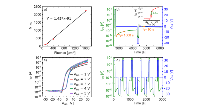
For our analysis, we first evaluate the memory window, i.e., the height of the hysteresis (i.e. at the same ) for the different irradiation fluences. The results found for our different devices are summarized in Figure 4 a). The hysteresis’ height increases linearly with increasing ion fluence reaching up to around two orders of magnitude for the device irradiated with the highest fluence. We note, that even for the smallest irradiation fluence of only 100 ions/m2 there is already a fully developed hysteresis observable even though it was nearly absent prior to the irradiation (see Figure S2). These results clearly demonstrate, that ion induced defects are responsible for the observed hysteresis.
To study the switching behavior of our device we applied 30 V gate pulses and recorded the transient behavior of the device irradiated with a fluence of 200 ions/m2. The result is shown in Figure 4 b). In this device we can reach two distinct memory states at a gate voltage of = 0 V with a current separation of around one order of magnitude. The current separation prevails and is stable for the entire observed pulse interval (around 30 min), which is comparable with the rentention times observed in few-layer MoS2 charge-trapping memory devices 80, 81. The transients observed in Fig. 4 b) can be interpreted in terms of charge trapping/detrapping mechanisms. The time constants have been evaluated for the read () and the erase () configuration by fitting an exponential function to the data.
Compared to previous studies, the time constants = 1600 s and = 90 s, respectively, are rather long15. This finding points towards oxide defects playing a major role because charges trapped in deep oxide defects have considerably longer relaxation times than e.g. traps in the 2D material itself or at the 2D material/oxide interface 82, 83, 21. The time constant for the positive gate pulse () is much longer than the time constant for negative gate pulse (). This is also another indicator of negatively charged oxide defects being the main contribution to the hysteresis in our work. These defects lie in the vicinity of the conduction band of MoS2 63 and would therefore be charged when applying positive gate voltages, but would not be charged for the negative gate pulse. Additionally, we show in Figure 4 c) that the observed hysteresis is independent on the applied within the range of 1 V - 5 V. This is in contrast to recent observations for black phosphorous FETs, where the dependence of the hysteresis on was ascribed to defects in the 2D material channel itself 84.
Considering our irradiation conditions, significant defect generation in the substrate is to be expected. In Figure S1 b) we show a SRIM 85 calculation of our sample system with a monolayer placed on top of a layer irradiated with ions with a kinetic energy of 180 keV. Most of the collisions caused by ion irradiation at this kinetic energy occur in the oxide, since the channel is atomically thin.
We therefore conclude, that while the doping effect may be due to both, ion-induced defects in the MoS2 and the substrate, the hysteresis observed in our devices is caused by negatively charged defects in the underlying oxide induced by the HCI irradiation.
With Figure 4 d) we prove that the separation of the two memory states is stable for several memory cycles.
3 Conclusion
We have investigated the manipulation of the electrical properties of FETs by the irradiation with HCIs. While we found a decreasing mobility in the devices with increasing ion fluence, the conductivity after an initial drop actually increases with higher defect density suggesting that at hopping-like transport takes over with increasing defect density. This further proves, that the devices are rather resistant to ion irradiation, an important factor for the possible use in high radiation environments like e.g. space applications. Additionally, we have shown that HCI irradiation can be used for deliberate and controlled manipulation of the doping density of devices. In our case we found a strong decrease in n-doping. Most notably, the irradiation leads to a hysteresis in the transfer characteristics of the device which we successfully exploited for a non-volatile memory device with two stable memory states and a long retention time. We demonstrated that the memory window can be tuned by the irradiation fluence, opening up new possibilities to boost the performance of based memory devices. We also believe, that this procedure can be applied to other similar 2D devices since the hysteresis probably originates from defects induced into the underlying oxide. In future experiments, it should be possible to precisely control the creation of defects and fine-tune the electrical properties through ion irradiation by independently controlling the potential and kinetic energy of the ions. This level of control would enable us to determine the specific locations where defects are created and thereby precisely manipulate the electrical properties of the irradiated devices.
4 Experimental Procedure
flakes were grown via chemical vapor deposition (CVD) on a highly doped p-type Si substrate (resistivity 0.001-0.005 cm) covered by 285 nm thermal . At first a 1 % sodium cholate solution was spin coated onto the substrate working as a seeding promoter. The growth was performed in a three-zone (ThermConcept ROK 70/750/12-3z) tube furnace. By 10 min purging with 500 sccm Ar gas (99.9 %) flow, the content of the furnace was minimized. 40 mg of S powder (99.98 % Sigma Aldrich) were placed in the upstream heating zone at 150 ∘C. , used as the source for molybdenum, was obtained from a aqueous ammonium heptamolybdate (AHM) solution (ratio 1:1) initially annealed at 300 ∘C for 24 min under ambient conditions and positioned in the next downstream zone at 750 ∘C. During the whole process 500 sccm of Ar gas flows through the quartz tube. The growth process lasted 30 min and was followed by a rapid cooling. At a temperature of around 100 ∘C the samples were retrieved from the CVD furnace. The resulting flakes are mostly single layers with triangular shape.
For device fabrication the freshly grown samples were investigated via optical microscopy to select suitable flakes for photolithography processing. After the standard photolithography process 10 nm of Cr and 100 nm of Au were deposited by electron-beam (Cr) and thermal evaporation (Au) at a process pressure of mbar to electrically contact the flakes.
Electrical characterization of the devices was performed with a cryogenic probe station with pressure control and four metallic nanoprobes, which are connected to a Keithley 4200 SCS. The metallic sample plate was used to apply the backgate voltage to the Si substrate. All electrical measurements in this work are performed under a vacuum of mbar and the samples were left there for at least 12 hours before starting the measurements.
To irradiate the samples, highly charged xenon ions were generated in an electron beam ion source (EBIS) commercially available from Dreebit GmbH, Germany 86. A kinetic energy of 180 keV (1.4 keV/amu) and an ion charge state of with a potential energy of 15.4 keV (0.1 keV/amu) was selected via a sector magnet and used for all experiments. Ion irradiation was performed under ultra-high vacuum conditions (pressure about mbar), and each sample was irradiated with a total fluence between 100 and 1600 ions/m2.
Author Contributions
St.S., M.S. and A.d.B. are responsible for the conceptualization of the project and the experiments. St.S., A.P. and E.F. performed the investigation. St.S. analyzed and evaluated the data. L.S. performed the irradiation and helped with data interpretation. O.K., A.M. and Y.L. did the the device fabrication. M.S. and A.d.B. were responsible for funding acquisition and provided resources. St.S was responsible for writing the original draft. All authors contributed to the writing by reviewing and editing the manuscript.
Conflicts of interest
There are no conflicts to declare.
Acknowledgments
This work was funded by the Deutsche Forschungsgemeinschaft (DFG, German Research Foundation - project numbers INST-272132938, INST-429784087, 406129719 and 461605777 (IRTG 2038 2D MATURE) and the Bundesministerium für Bildung und Forschung (BMBF, project number 05K16PG1). We acknowledge support by the clean room staff of A. Lorke, especially G. Prinz.
Notes and references
- Kam and Parkinson 1982 K. K. Kam and B. A. Parkinson, The Journal of Physical Chemistry, 1982, 86, 463–467.
- Mak et al. 2010 K. F. Mak, C. Lee, J. Hone, J. Shan and T. F. Heinz, Physical review letters, 2010, 105, 136805.
- Radisavljevic et al. 2011 B. Radisavljevic, A. Radenovic, J. Brivio, V. Giacometti and A. Kis, Nature nanotechnology, 2011, 6, 147–150.
- Uchida et al. 2002 K. Uchida, H. Watanabe, A. Kinoshita, J. Koga, T. Numata and S. Takagi, Digest. International Electron Devices Meeting, 2002.
- Gomez et al. 2007 L. Gomez, I. berg and J. L. Hoyt, IEEE Electron Device Letters, 2007, 28, 285–287.
- Schmidt et al. 2009 M. Schmidt, M. C. Lemme, H. Gottlob, F. Driussi, L. Selmi and H. Kurz, Solid-State Electronics, 2009, 53, 1246–1251.
- English et al. 2016 C. D. English, G. Shine, V. E. Dorgan, K. C. Saraswat and E. Pop, Nano Letters, 2016, 16, 3824–3830.
- English et al. 2016 C. D. English, K. K. H. Smithe, R. L. Xu and E. Pop, 2016 International Electron Devices Meeting, Piscataway, NJ, 2016, pp. 5.6.1–5.6.4.
- Desai et al. 2016 S. B. Desai, S. R. Madhvapathy, A. B. Sachid, J. P. Llinas, Q. Wang, G. H. Ahn, G. Pitner, M. J. Kim, J. Bokor, C. Hu, H.-S. P. Wong and A. Javey, Science, 2016, 354, 99–102.
- Schulman et al. 2018 D. S. Schulman, A. J. Arnold and S. Das, Chemical Society reviews, 2018, 47, 3037–3058.
- Grillo and Di Bartolomeo 2021 A. Grillo and A. Di Bartolomeo, Advanced Electronic Materials, 2021, 7, 2000979.
- He et al. 2019 Q. He, Y. Liu, C. Tan, W. Zhai, G.-H. Nam and H. Zhang, ACS nano, 2019, 13, 12294–12300.
- Knobloch et al. 2022 T. Knobloch, S. Selberherr and T. Grasser, Nanomaterials, 2022, 12, 3548.
- Late et al. 2012 D. J. Late, B. Liu, H. S. S. R. Matte, V. P. Dravid and C. N. R. Rao, ACS nano, 2012, 6, 5635–5641.
- Urban et al. 2019 F. Urban, F. Giubileo, A. Grillo, L. Iemmo, G. Luongo, M. Passacantando, T. Foller, L. Madauß, E. Pollmann, M. P. Geller, D. Oing, M. Schleberger and A. Di Bartolomeo, 2D Materials, 2019, 6, 045049.
- Di Bartolomeo et al. 2018 A. Di Bartolomeo, L. Genovese, F. Giubileo, L. Iemmo, G. Luongo, T. Foller and M. Schleberger, 2D Materials, 2018, 5, 015014.
- Shu et al. 2016 J. Shu, G. Wu, Y. Guo, B. Liu, X. Wei and Q. Chen, Nanoscale, 2016, 8, 3049–3056.
- Faella et al. 2022 E. Faella, K. Intonti, L. Viscardi, F. Giubileo, A. Kumar, H. T. Lam, K. Anastasiou, M. F. Craciun, S. Russo and A. Di Bartolomeo, Nanomaterials, 2022, 12, 1886.
- Bertolazzi et al. 2013 S. Bertolazzi, D. Krasnozhon and A. Kis, ACS nano, 2013, 7, 3246–3252.
- He et al. 2016 G. He, H. Ramamoorthy, C.-P. Kwan, Y.-H. Lee, J. Nathawat, R. Somphonsane, M. Matsunaga, A. Higuchi, T. Yamanaka, N. Aoki, Y. Gong, X. Zhang, R. Vajtai, P. M. Ajayan and J. P. Bird, Nano Letters, 2016, 16, 6445–6451.
- Kaushik et al. 2017 N. Kaushik, D. M. A. Mackenzie, K. Thakar, N. Goyal, B. Mukherjee, P. Boggild, D. H. Petersen and S. Lodha, npj 2D Materials and Applications, 2017, 1, 34.
- Komsa et al. 2013 H.-P. Komsa, S. Kurasch, O. Lehtinen, U. Kaiser and A. V. Krasheninnikov, Physical Review B, 2013, 88, 035301.
- Jin et al. 2009 C. Jin, F. Lin, K. Suenaga and S. Iijima, Physical review letters, 2009, 102, 195505.
- Li and Chen 2017 Z. Li and F. Chen, Applied Physics Reviews, 2017, 4, 011103.
- Madauß et al. 2017 L. Madauß, O. Ochedowski, H. Lebius, B. Ban-d’Etat, C. H. Naylor, A. T. C. Johnson, J. Kotakoski and M. Schleberger, 2D Materials, 2017, 4, 015034.
- Ochedowski et al. 2014 O. Ochedowski, H. Bukowska, V. M. Freire Soler, L. Brökers, B. Ban-d’Etat, H. Lebius and M. Schleberger, Nuclear Instruments and Methods in Physics Research Section B: Beam Interactions with Materials and Atoms, 2014, 340, 39–43.
- Kotakoski et al. 2015 J. Kotakoski, C. Brand, Y. Lilach, O. Cheshnovsky, C. Mangler, M. Arndt and J. C. Meyer, Nano Letters, 2015, 15, 5944–5949.
- Cohen-Tanugi and Grossman 2012 D. Cohen-Tanugi and J. C. Grossman, Nano Letters, 2012, 12, 3602–3608.
- Madauß et al. 2017 L. Madauß, J. Schumacher, M. Ghosh, O. Ochedowski, J. Meyer, H. Lebius, B. Ban-d’Etat, M. E. Toimil-Molares, C. Trautmann, R. G. H. Lammertink, M. Ulbricht and M. Schleberger, Nanoscale, 2017, 9, 10487–10493.
- Postma 2010 H. W. C. Postma, Nano Letters, 2010, 10, 420–425.
- Kozubek et al. 2018 R. Kozubek, P. Ernst, C. Herbig, T. Michely and M. Schleberger, ACS Applied Nano Materials, 2018, 1, 3765–3773.
- Madauß et al. 2018 L. Madauß, I. Zegkinoglou, H. Vázquez Muiños, Y.-W. Choi, S. Kunze, M.-Q. Zhao, C. H. Naylor, P. Ernst, E. Pollmann, O. Ochedowski, H. Lebius, A. Benyagoub, B. Ban-d’Etat, A. T. C. Johnson, F. Djurabekova, B. Roldan Cuenya and M. Schleberger, Nanoscale, 2018, 10, 22908–22916.
- Brennan et al. 2021 B. Brennan, A. Centeno, A. Zurutuza, P. Mack, K. R. Paton and A. J. Pollard, ACS Applied Nano Materials, 2021, 4, 5187–5197.
- Sleziona et al. 2021 S. Sleziona, S. Rauls, T. Heckhoff, L. Christen, E. Pollmann, L. Madauß, S. Franzka, A. Lorke, H. Wende and M. Schleberger, Nanotechnology, 2021, 32, 205702.
- Stanford et al. 2016 M. G. Stanford, P. R. Pudasaini, A. Belianinov, N. Cross, J. H. Noh, M. R. Koehler, D. G. Mandrus, G. Duscher, A. J. Rondinone, I. N. Ivanov, T. Z. Ward and P. D. Rack, Scientific reports, 2016, 6, 27276.
- Zion et al. 2015 E. Zion, A. Haran, A. Butenko, L. Wolfson, Y. Kaganovskii, T. Havdala, A. Sharoni, D. Naveh, V. Richter, M. Kaveh, E. Kogan and I. Shlimak, Graphene, 2015, 04, 45–53.
- Li et al. 2019 H. Li, C. Liu, Y. Zhang, C. Qi, Y. Wei, J. Zhou, T. Wang, G. Ma, H.-S. Tsai, S. Dong and M. Huo, Nanotechnology, 2019, 30, 485201.
- Bertolazzi et al. 2017 S. Bertolazzi, S. Bonacchi, G. Nan, A. Pershin, D. Beljonne and P. Samorì, Advanced Materials, 2017, 29, 1606760.
- Ernst et al. 2016 P. Ernst, R. Kozubek, L. Madauß, J. Sonntag, A. Lorke and M. Schleberger, Nuclear Instruments and Methods in Physics Research Section B: Beam Interactions with Materials and Atoms, 2016, 382, 71–75.
- Kumar et al. 2018 S. Kumar, A. Kumar, A. Tripathi, C. Tyagi and D. K. Avasthi, Journal of Applied Physics, 2018, 123, 161533.
- Ochedowski et al. 2013 O. Ochedowski, K. Marinov, G. Wilbs, G. Keller, N. Scheuschner, D. Severin, M. Bender, J. Maultzsch, F. J. Tegude and M. Schleberger, Journal of Applied Physics, 2013, 113, 214306.
- Skopinski et al. 2023 L. Skopinski, S. Kretschmer, P. Ernst, M. Herder, L. Madauß, L. Breuer, A. V. Krasheninnikov and M. Schleberger, Physical Review B, 2023, 107, 044003.
- Lee et al. 2010 C. Lee, H. Yan, L. E. Brus, T. F. Heinz, J. Hone and S. Ryu, ACS nano, 2010, 4, 2695–2700.
- Kim et al. 2017 C. Kim, I. Moon, D. Lee, M. S. Choi, F. Ahmed, S. Nam, Y. Cho, H.-J. Shin, S. Park and W. J. Yoo, ACS nano, 2017, 11, 1588–1596.
- Jung et al. 2019 Y. Jung, M. S. Choi, A. Nipane, A. Borah, B. Kim, A. Zangiabadi, T. Taniguchi, K. Watanabe, W. J. Yoo, J. Hone and J. T. Teherani, Nature Electronics, 2019, 2, 187–194.
- Guo et al. 2015 Y. Guo, D. Liu and J. Robertson, ACS Applied Materials & Interfaces, 2015, 7, 25709–25715.
- Smyth et al. 2016 C. M. Smyth, R. Addou, S. McDonnell, C. L. Hinkle and R. M. Wallace, The Journal of Physical Chemistry C, 2016, 120, 14719–14729.
- Saidi 2014 W. A. Saidi, The Journal of Chemical Physics, 2014, 141, 094707.
- Di Bartolomeo et al. 2018 A. Di Bartolomeo, A. Grillo, F. Urban, L. Iemmo, F. Giubileo, G. Luongo, G. Amato, L. Croin, L. Sun, S.-J. Liang and L. K. Ang, Advanced Functional Materials, 2018, 28, 1800657.
- Qiu et al. 2013 H. Qiu, T. Xu, Z. Wang, W. Ren, H. Nan, Z. Ni, Q. Chen, S. Yuan, F. Miao, F. Song, G. Long, Y. Shi, L. Sun, J. Wang and X. Wang, Nature communications, 2013, 4, 2642.
- Suh et al. 2014 J. Suh, T.-E. Park, D.-Y. Lin, D. Fu, J. Park, H. J. Jung, Y. Chen, C. Ko, C. Jang, Y. Sun, R. Sinclair, J. Chang, S. Tongay and J. Wu, Nano Letters, 2014, 14, 6976–6982.
- Tongay et al. 2013 S. Tongay, J. Suh, C. Ataca, W. Fan, A. Luce, J. S. Kang, J. Liu, C. Ko, R. Raghunathanan, J. Zhou, F. Ogletree, J. Li, J. C. Grossman and J. Wu, Scientific reports, 2013, 3, 2657.
- McDonnell et al. 2014 S. McDonnell, R. Addou, C. Buie, R. M. Wallace and C. L. Hinkle, ACS nano, 2014, 8, 2880–2888.
- Liu et al. 2018 Y. Liu, J. Guo, E. Zhu, L. Liao, S.-J. Lee, M. Ding, I. Shakir, V. Gambin, Y. Huang and X. Duan, Nature, 2018, 557, 696–700.
- Pelella et al. 2020 A. Pelella, O. Kharsah, A. Grillo, F. Urban, M. Passacantando, F. Giubileo, L. Iemmo, S. Sleziona, E. Pollmann, L. Madauß, M. Schleberger and A. Di Bartolomeo, ACS Applied Materials & Interfaces, 2020, 12, 40532–40540.
- Shahzad et al. 2019 K. Shahzad, K. Jia, C. Zhao, D. Wang, M. Usman and J. Luo, Materials, 2019, 12, 3928.
- Lehtinen et al. 2011 O. Lehtinen, J. Kotakoski, A. V. Krasheninnikov and J. Keinonen, Nanotechnology, 2011, 22, 175306.
- Lehtinen et al. 2010 O. Lehtinen, J. Kotakoski, A. V. Krasheninnikov, A. Tolvanen, K. Nordlund and J. Keinonen, Physical Review B, 2010, 81, 153401.
- Zhou et al. 2013 W. Zhou, X. Zou, S. Najmaei, Z. Liu, Y. Shi, J. Kong, J. Lou, P. M. Ajayan, B. I. Yakobson and J.-C. Idrobo, Nano Letters, 2013, 13, 2615–2622.
- Schleberger and Kotakoski 2018 M. Schleberger and J. Kotakoski, Materials , 2018, 11, 1885.
- Kozubek et al. 2019 R. Kozubek, M. Tripathi, M. Ghorbani-Asl, S. Kretschmer, L. Madauß, E. Pollmann, M. O’Brien, N. McEvoy, U. Ludacka, T. Susi, G. S. Duesberg, R. A. Wilhelm, A. V. Krasheninnikov, J. Kotakoski and M. Schleberger, The journal of physical chemistry letters, 2019, 10, 904–910.
- Ghaderzadeh et al. 2020 S. Ghaderzadeh, V. Ladygin, M. Ghorbani-Asl, G. Hlawacek, M. Schleberger and A. V. Krasheninnikov, ACS Applied Materials & Interfaces, 2020, 12, 37454–37463.
- Knobloch et al. 2018 T. Knobloch, G. Rzepa, Y. Y. Illarionov, M. Waltl, F. Schanovsky, B. Stampfer, M. M. Furchi, T. Mueller and T. Grasser, IEEE Journal of the Electron Devices Society, 2018, 6, 972–978.
- Nan et al. 2014 H. Nan, Z. Wang, W. Wang, Z. Liang, Y. Lu, Q. Chen, D. He, P. Tan, F. Miao, X. Wang, J. Wang and Z. Ni, ACS nano, 2014, 8, 5738–5745.
- Tongay et al. 2013 S. Tongay, J. Zhou, C. Ataca, J. Liu, J. S. Kang, T. S. Matthews, L. You, J. Li, J. C. Grossman and J. Wu, Nano Letters, 2013, 13, 2831–2836.
- Wang et al. 2022 S. Wang, X. Zeng, Y. Zhou, J. Lu, Y. Hu, W. Wang, J. Wang, Y. Xiao, X. Wang, D. Chen, T. Xu, M. Zhang and X. Bao, ACS Applied Electronic Materials, 2022, 4, 955–963.
- Wei et al. 2014 X. Wei, Z. Yu, F. Hu, Y. Cheng, L. Yu, X. Wang, M. Xiao, J. Wang, X. Wang and Y. Shi, AIP Advances, 2014, 4, 123004.
- Kong et al. 2014 L. Kong, A. Enders, T. S. Rahman and P. A. Dowben, Journal of physics. Condensed matter : An Institute of Physics journal, 2014, 26, 443001.
- KC et al. 2015 S. KC, R. C. Longo, R. M. Wallace and K. Cho, Journal of Applied Physics, 2015, 117, 135301.
- Degraeve et al. 2008 R. Degraeve, M. Cho, B. Govoreanu, B. Kaczer, M. B. Zahid, J. van Houdt, M. Jurczak and G. Groeseneken, IEEE International Electron Devices Meeting, 2008, Piscataway, NJ, 2008, pp. 1–4.
- Illarionov et al. 2017 Y. Y. Illarionov, T. Knobloch, M. Waltl, G. Rzepa, A. Pospischil, D. K. Polyushkin, M. M. Furchi, T. Mueller and T. Grasser, 2D Materials, 2017, 4, 025108.
- Huang et al. 2020 K. Huang, M. Zhao, B. Sun, X. Liu, J. Liu, H. Chang, Y. Zeng and H. Liu, ACS Applied Electronic Materials, 2020, 2, 971–979.
- Novoselov et al. 2005 K. S. Novoselov, D. Jiang, F. Schedin, T. J. Booth, V. V. Khotkevich, S. V. Morozov and A. K. Geim, Proceedings of the National Academy of Sciences of the United States of America, 2005, 102, 10451–10453.
- Amani et al. 2013 M. Amani, M. L. Chin, A. G. Birdwell, T. P. O’Regan, S. Najmaei, Z. Liu, P. M. Ajayan, J. Lou and M. Dubey, Applied Physics Letters, 2013, 102, 193107.
- Chakraborty et al. 2012 B. Chakraborty, A. Bera, D. V. S. Muthu, S. Bhowmick, U. V. Waghmare and A. K. Sood, Physical Review B, 2012, 85, 161403.
- Pollmann et al. 2020 E. Pollmann, L. Madauß, S. Schumacher, U. Kumar, F. Heuvel, C. vom Ende, S. Yilmaz, S. Güngörmüs and M. Schleberger, Nanotechnology, 2020, 31, 505604.
- Guo et al. 2015 Y. Guo, X. Wei, J. Shu, B. Liu, J. Yin, C. Guan, Y. Han, S. Gao and Q. Chen, Applied Physics Letters, 2015, 106, 103109.
- Choi et al. 2015 K. Choi, S. R. A. Raza, H. S. Lee, P. J. Jeon, A. Pezeshki, S.-W. Min, J. S. Kim, W. Yoon, S.-Y. Ju, K. Lee and S. Im, Nanoscale, 2015, 7, 5617–5623.
- Illarionov et al. 2016 Y. Y. Illarionov, G. Rzepa, M. Waltl, T. Knobloch, A. Grill, M. M. Furchi, T. Mueller and T. Grasser, 2D Materials, 2016, 3, 035004.
- Zhang et al. 2015 E. Zhang, W. Wang, C. Zhang, Y. Jin, G. Zhu, Q. Sun, D. W. Zhang, P. Zhou and F. Xiu, ACS nano, 2015, 9, 612–619.
- Hou et al. 2018 X. Hou, X. Yan, C. Liu, S. Ding, D. W. Zhang and P. Zhou, Semiconductor Science and Technology, 2018, 33, 034001.
- Nagumo et al. 06.12.2010 - 08.12.2010 T. Nagumo, K. Takeuchi, T. Hase and Y. Hayashi, 2010 International Electron Devices Meeting, 06.12.2010 - 08.12.2010, pp. 28.3.1–28.3.4.
- Lee et al. 2011 Y. G. Lee, C. G. Kang, U. J. Jung, J. J. Kim, H. J. Hwang, H.-J. Chung, S. Seo, R. Choi and B. H. Lee, Applied Physics Letters, 2011, 98, 183508.
- Kumar et al. 2023 A. Kumar, L. Viscardi, E. Faella, F. Giubileo, K. Intonti, A. Pelella, S. Sleziona, O. Kharsah, M. Schleberger and A. Di Bartolomeo, Journal of Materials Science, 2023, 58, 2689–2699.
- Ziegler et al. 2010 J. F. Ziegler, M. D. Ziegler and J. P. Biersack, Nuclear Instruments and Methods in Physics Research Section B: Beam Interactions with Materials and Atoms, 2010, 268, 1818–1823.
- Zschornack et al. 2008 G. Zschornack, M. Kreller, V. P. Ovsyannikov, F. Grossman, U. Kentsch, M. Schmidt, F. Ullmann and R. Heller, The Review of scientific instruments, 2008, 79, 02A703.