Piezoelectric altermagnetism and spin-valley polarization in Janus monolayer
Abstract
The altermagnetism can achieve spin-split bands in collinear symmetry-compensated antiferromagnets. Here, we predict altermagnetic order in Janus monolayer with eliminated inversion symmetry, which can realize the combination of piezoelectricity and altermagnetism in a two-dimensional material, namely 2D piezoelectric altermagnetism. It is found that is an altermagnetic semiconductor, and the spin-split bands of both valence and conduction bands are near the Fermi level. The has large out-of-plane piezoelectricity (0.97 pm/V), which is highly desirable for ultrathin piezoelectric device application. Due to spin-valley locking, both spin and valley can be polarized by simply breaking the corresponding crystal symmetry with uniaxial strain. Our findings provide a platform to integrate spin, piezoelectricity and valley in a single material, which is useful for multi-functional device applications.
I Introduction
The antiferromagnetic (AFM) materials do not have any net magnetic moment, which are robust to external magnetic perturbation, and have ultra-high dynamic speed, allowing high-speed device operationk1 ; k2 . However, it is often hard to realize spin-polarized currents in collinear AFM systems because of the missing spin-splitting in the band structuresk3 . Recently, the spin-splitting has been achieved in collinear symmetry-compensated antiferromagnets, be called altermagnetismk4 ; k5 ; k6 . The spin-splitting is only originated from the simple AFM order with special magnetic space group, and the relativistic spin-orbital coupling (SOC) is thus not needed. Several bulk materials have been predicted to be altermagnetism, such as k7 , k7-1 , MnTek7-2 , some organic AFMsk8 , k9 and some -type perovskitesk10 .
Besides, several two-dimensional (2D) materials have also been predicted to have this spin-splitting with special AFM order, such as k11 ; k12 and k13 . However, these 2D altermagnetic materials have inversion symmetry, leading to missing piezoelectricity. Searching for 2D piezoelectric altermagnetism (PAM) may be significative and challenging. In fact, many 2D piezoelectric ferromagnetisms (PFMs) has been predictedq15-0 ; q15-1 ; q15-2 ; q15-3 ; q15-4 , which achieve the combination of piezoelectricity and ferromagnetic (FM) order in a 2D material. Most of these 2D PFMs possess Janus structure, which can destroy out-of-plane symmetry, inducing out-of-plane piezoelectricity. Therefore, 2D Janus materials may provide a potential platform for searching 2D PAMs. Another question is how to achieve spin polarization in 2D altermagnetic materials, and strain may be a very effective way to induce spin polarizationk11 ; k12 ; k13 .
Here, we construct Janus monolayer as derivative of altermagnetic monolayer. Calculated results show that is still a 2D altermagnetic material, and has large out-of-plane piezoelectricity, which achieves PAM. Both spin and valley polarizations can be realized by simply breaking the corresponding crystal symmetry with uniaxial strain. Compared with existing 2D altermagnetic k11 ; k12 and k13 , has two main differences: (1) it has large out-of-plane piezoelectricity; (2) near the Fermi level, the states of conduction and valence bands around X or Y high-symmetry point are with opposite spins.
II Computational detail
We perform the spin-polarized first-principles calculations within density functional theory (DFT)1 by using the standard VASP packagepv1 ; pv2 ; pv3 within the projector augmented-wave (PAW) method. The generalized gradient approximation of Perdew-Burke-Ernzerhof (PBE-GGA)pbe is used as the exchange-correlation functional. We set kinetic energy cutoff of 500 eV, total energy convergence criterion of eV, and force convergence criterion of 0.0001 . To account for electron correlation of Cr-3 orbitals, a Hubbard correction =3.55 eVk11 ; k12 is employed within the rotationally invariant approach proposed by Dudarev et al. The out-of-plane interaction is avoided by taking a vacuum of more than 16 . We use a 18181 Monkhorst-Pack k-point meshes to sample the Brillouin zone (BZ) for calculating electronic structures, elastic and piezoelectric properties.
The elastic stiffness tensor are calculated by using strain-stress relationship (SSR) method. The piezoelectric stress tensor are calculated by density functional perturbation theory (DFPT) methodpv6 . The / have been renormalized by =/=, where the is the length of unit cell along direction. Based on finite displacement method, the interatomic force constants (IFCs) are calculated by using 551 supercell, and the phonon dispersion spectrum is obtained by the Phonopy codepv5 . The ab-initio molecular dynamics (AIMD) simulations using NVT ensemble are performed for more than 8000 fs with a time step of 1 fs by using a 441 supercell. The elastic, piezoelectric, phonon and AIMD calculations are all carried out with altermagnetic order.

III Crystal structure and stability
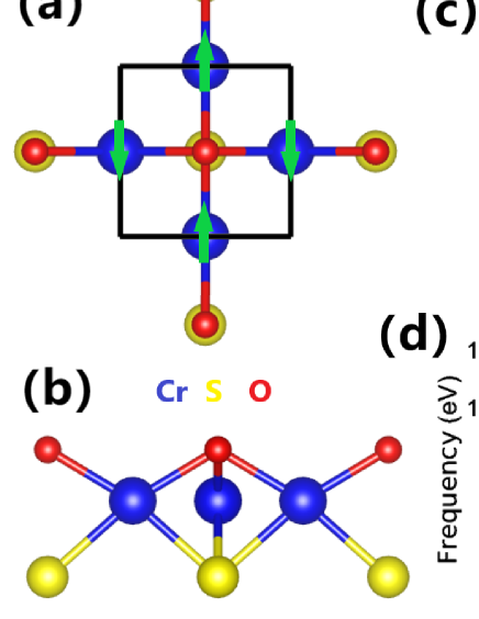
Monolayer and have similar crystal structures, and they contain three atomic sublayers with two co-planar Cr atoms as middle layer and O/S atoms as upper and lower layers. The Janus monolayer can be constructed by replacing one of two O layers with S atoms in monolayer . The schematic crystal structures of are shown in Figure 1 (a) and (b). The monolayer possesses space group (No.123)k11 ; k12 , and the monolayer crystallizes in the space group (No.99). For monolayer , the key space-group symmetry operations contain space inversion , rotation and /// mirror, indicating no piezoelectricity. With respect to , the and of are removed, which means that the will be piezoelectric. In one unit cell, the FM and AFM configurations are constructed to determine magnetic ground state and lattice constants. Calculated results show that the AFM configuration is ground state of , and its energy is 1.122 eV lower than that of FM case within GGA+. The optimized lattice constants ==3.66 by GGA+ for AFM case. The magnetic easy-axis is investigated by calculating the energy difference of the magnetization orientation along the (100) and (001) cases, which is defined as magnetic anisotropy energy (MAE). Calculated results show that the MAE is -93 /Fe, which indicates that the easy-axis of is in-plane.
To evaluate the stability of , the phonon dispersion, molecular dynamics and elastic constants are calculated by using GGA+ for AFM case. The phonon dispersions of are shown in Figure 1 (d), and no imaginary frequencies can be observed, indicating its dynamic stability. To corroborate the thermal stability, the evolution of total energy vs time are calculated using AIMD at 200 and 300 K, which are shown in FIG.1 and FIG.2 of electronic supplementary information (ESI). At 200 K, the energies are kept stable, and the crystal features are preserved after 8 ps, which confirms its thermal stability. However, at 300 K, the thermal stability of is broken. The independent elastic constants , and of are 64.93 , 37.26 and 30.05 , which satisfy the Born criteria of mechanical stability: , , , confirming its mechanical stability.
IV electronic structures
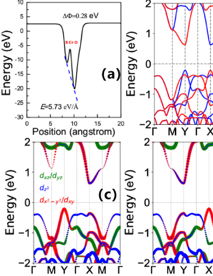
The planar average of the electrostatic potential energy along out-of-plane direction is shown in Figure 2 (a). Due to mirror asymmetry, an electrostatic potential gradient () of about 0.28 eV is produced, which is related to the work function change of the structure. Due to the electron redistribution, there is an inherent electric field with the magnitude of about 5.73 , implying a very strong vertical polarization in the monolayer.
The Cr atoms in monolayer possess a local magnetic moment around 3.46 , and the two Cr-atom sublattices with the 2D AFM order are related by mirror symmetry but cannot be transformed to each other by any translation operation, which leads to existing altermagnetism. The energy band structures of are plotted in Figure 2 (b) by GGA+U method without SOC. There are two valleys at X and Y high-symmetry points for both conduction and valence bands, which are related by the mirror symmetry. States around X and Y points are mainly from two different Cr atoms with opposite spins due to the AFM order, producing altermagnetism in the absence of SOC and spin-valley locking. Compared with spin-gapless k11 ; k12 , it is clearly seen that is a direct band gap semiconductor with gap value of 0.838 eV, which may be due to strong inherent electric field (5.73 ). The valence band maximum (VBM) and conduction band bottom (CBM) of are at high symmetry X or Y point, while those of deviate from X or Y point. Near the Fermi level, states of conduction and valence bands around X or Y point are from two different Cr atoms with opposite spins, while those of are with the same spinsk11 ; k12 . For monolayer, the same spins are also observed for states of conduction and valence bands around X or Y point near the Fermi levelk13 . According to Figure 2 (b) and (d), it is found that ++ orbitals dominate X and Y valleys of conduction bands, and the X and Y valleys of valence bands are mainly from + orbitals.
The electronic correlation effects on electronic structures of are considered by using different values. Firstly, the lattice constants at different (0-4 eV) are optimized, and then calculate electronic properties of . With increasing , the lattice constants increases, and its change is about 0.232 . According to FIG.3 of ESI, it is found that is always a AFM ground state. The evolutions of energy band structures as a function of are calculated, which are plotted in FIG.4 of ESI. With increasing the , monolayer experiences a phase transition from metal to semiconductor, and the critical point is about 2 eV. Similar phenomenon can be also observed in monolayer k13 . For 2 eV, near the Fermi level, states of conduction and valence bands around X or Y point are always from two different Cr atoms with opposite spins.


V Piezoelectric properties
Due to inversion symmetry, the monolayer possesses no piezoelectricity. However, the monolayer has piezoelectricity with missing and symmetries. Namely, the reflectional symmetry of disappears across the plane, but holds across the or plane, which leads to existing out-of-plane piezoelectricity and missing in-plane piezoelectricity. The third-rank piezoelectric stress tensor and strain tensor can be used to describe the piezoelectric response of a material. They can be expressed as the sum of ionic and electronic contributions:
| (1) |
Where , and are polarization vector, strain and stress, respectively. The superscripts and mean electronic and ionic contributions. The and ( and ) are also called clamped-ion (relaxed-ion) piezoelectric coefficients. The is related with by elastic tensor :
| (2) |
By using Voigt notation, only considering the in-plane strain and stresso2 , the Equation 2 can be reduced into:
| (3) |
The existing / means that only vertical piezoelectric polarization can be induced, when a uniaxial strain is applied. By solving the Equation 3, the can be obtained:
| (4) |
The primitive cell is used to calculate the of monolayer . The calculated is -0.987 with ionic part 0.111 and electronic part -1.098. The electronic and ionic contributions have opposite signs, and the electronic part dominates the piezoelectricity. And then, the can be attained from Equation 4, and the corresponding value is -0.97 pm/V. The minus sign depends on the choice of coordinate system. If the directions are reversed, the will become 0.97 pm/V. A large out-of-plane piezoelectric response () is very important to be compatible with the nowadays bottom/top gate technologies. The of is compared with or higher than ones of many known 2D materials, like functionalized h-BN (0.13 pm/V)o1 , kalium decorated graphene (0.3 pm/V)o2 , the oxygen functionalized MXenes (0.40-0.78 pm/V)q9 , Janus group-III materials (0.46 pm/V)q7-6 , Janus BiTeI/SbTeI monolayer (0.37-0.66 pm/V)o3 , Janus monolayer transition metal dichalcogenides (0.03 pm/V)o3-1 and - (0.415 pm/V)o4 . The large may be related to large electronegativity difference of S and O atomsq15-3 ; q15-4 . The large provide possibility to tune spin-split bands of altermagnetic by piezoelectric effect.
VI uniaxial strain induces spin-valley polarization
To induce spin-valley polarization in , an experimentally feasible approach is to destroy symmetry by applying uniaxial strain along or direction, which will lead to nonequivalent X and Y valleys, giving rise to spin-valley polarization. We use (0.96 to 1.04) to simulate the uniaxial strain along direction, and the lattice constants along direction is optimized. The and are the strained and unstrained lattice constants with 1 (1) being compressive (tensile) case. If the strain is applied along direction, the opposite gap change and spin-valley polarization are exactly generated, since two valleys are related with symmetry. The Young’s modulus is calculated to elucidate mechanical performance of , which is plotted in FIG.5 of ESI. The calculated of along direction (44 ) is very small than those of many known 2D materials, such as graphene ( Nm-1) and MoS2 ( Nm-1) q5-1 ; q5-1-1 , indicating its better mechanical flexibility.
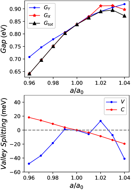
The energy differences () between AFM and FM states vs are calculated to determine the magnetic ground state of strained , which are plotted in FIG.6 of ESI. Within considered strain range, the is always negative, confirming that strained is AFM ground state. The energy band structures of strained monolayer are shown in Figure 3. The evolutions of related energy band gap (global gap [] and gaps of Y and X valleys [ and ]) and the valley splitting ( and ) for both valence and condition bands as a function of are plotted in Figure 4. For unstrained case, the global gap and gaps of and valleys are the same, indicating no valley polarization. It is found that both compressive and tensile strains can induce unequal gap between and valleys, which can produce valley polarization for both conduction and valence bands. It is clearly seen that compressive strain is in favour of separating and valleys of both conduction and valence bands from other bands, which makes for easily manipulating these valleys in experiment. At =0.96, the corresponding valley splitting are 18 meV (-48 meV) for conduction (valence) band.
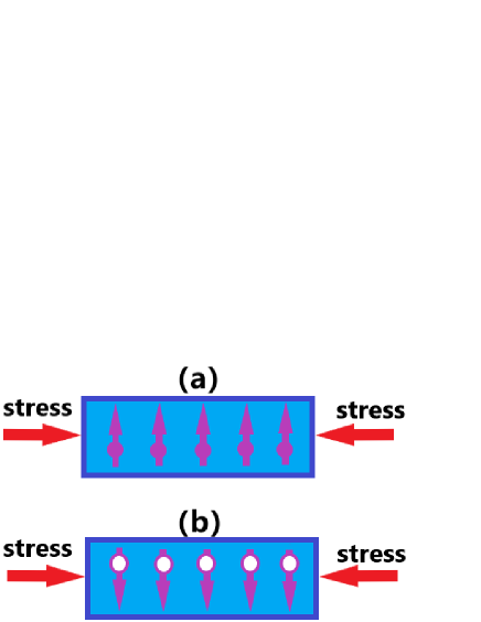
For compressive strain, an appropriate electron/hole doping can move the Fermi level to fall between the X and Y valleys, which leads to that only one valley has doped electron/holes. Due to spin-valley locking (see Figure 3 and Figure 5), the electron carriers possess spin-up character, while hole carriers have spin-down one. Upon appropriate doping, the magnetization can be produced due to the polarized carriers. The electron and hole doping leads to opposite magnetization direction. For a given electron/hole density, the magnetization can be tuned by uniaxial strain. These provide a platform for spin device applications.

VII Conclusion
In summary, we propose a 2D Janus altermagnetic material , which is dynamically, mechanically and thermally stable. Calculated results show that is a semiconductor with spin-split bands near the Fermi level. The structural symmetry-breaking and large electronegativity difference of O and S atoms lead to a large out-of-plane piezoelectric coefficient () of 0.97 pm/V. The possesses spin-valley locking, which is comprised of spin-polarized valleys related by a crystal symmetry. The spin-valley polarization can be induced by simply breaking the corresponding crystal symmetry with uniaxial strain. In fact, we provide a very effective method to induce piezoelectricity from centrosymmetric altermagnetism by constructing Janus structure. The method, analysis and results can be readily extended to other members of centrosymmetric monolayer altermagnetism AB (A = Co, Cr, Fe, Mn, Mo, Nb, Ni, Pd, Rh, Ru, Sc, Ti, V, Y, Zr; B = B, C, N, O, F, Al, Si, P, S, Cl, Ga, Ge, As, Se, Br), possessing the same structure and AFM magnetic configuration with k11 . Based on these altermagnetic monolayers, constructing Janus structure can realize piezoelectric altermagnetism.
Acknowledgements.
This work is supported by Natural Science Basis Research Plan in Shaanxi Province of China (2021JM-456). We are grateful to Shanxi Supercomputing Center of China, and the calculations were performed on TianHe-2..References
- (1) X. Hu, Adv. Mater. 24, 294 (2012).
- (2) T. Jungwirth, J. Sinova, A. Manchon, X. Marti, J. Wunderlich and C. Felser, Nat. Phys. 14, 200 (2018).
- (3) J. elezn, Y. Zhang, C. Felser and B. Yan, Phys. Rev. Lett. 119, 187204 (2017).
- (4) L. mejkal, J. Sinova and T. Jungwirth, Phys. Rev. X 12, 031042 (2022).
- (5) I. Mazin Phys. Rev. X 12, 040002 (2022).
- (6) L. mejkal, J. Sinova and T. Jungwirth, Phys. Rev. X 12, 040501 (2022).
- (7) L. mejkal, R. Gonzlez-Hernndez, T. Jungwirth and J. Sinova, Sci. Adv. 6, eaaz8809 (2020).
- (8) S. Lpez-Moreno, A. H. Romero, J. Meja-Lpez, A. Muoz and Igor V. Roshchin, Phys. Rev. B 85, 134110 (2012).
- (9) I. I. Mazin, Phys. Rev. B 107, L100418 (2023).
- (10) M. Naka, S. Hayami, H. Kusunose, Y. Yanagi, Y. Motome and H. Seo, Nat. Commun. 10, 4305 (2019).
- (11) L.-D. Yuan, Z. Wang, J.-W. Luo, E. I. Rashba and A. Zunger, Phys. Rev. B 102, 014422 (2020).
- (12) M. Naka, Y. Motome and H. Seo, Phys. Rev. B 103, 125114 (2021).
- (13) X. Chen, D. Wang, L. Y. Li and B. Sanyal, Preprint at https://arxiv.org/abs/2104.07390 (2021).
- (14) P. J. Guo, Z. X. Liu and Z. Y. Lu, npj Comput. Mater. 9, 70 (2023).
- (15) H.-Y. Ma, M. L. Hu, N. N. Li, J. P. Liu, W. Yao, J. F. Jia and J. W. Liu, Nat. Commun. 12, 2846 (2021).
- (16) G. Song, C. F. Zhang, Z. Z. Zhang, G. N. Li, Z. W. Li, J. Du, B. W. Zhang, X. K. Huang and B. L. Gao, Phys. Chem. Chem. Phys.24, 1091 (2022).
- (17) S. D. Guo, X. S. Guo, X. X. Cai, W. Q. Mu and W. C. Ren, J. Appl. Phys. 129, 214301 (2021).
- (18) G. Song, D. S. Li, H. F. Zhou et al., Appl. Phys. Lett. 118, 123102 (2021).
- (19) S. D. Guo, Y. T. Zhu, K. Qin and Y. S. Ang, Appl. Phys. Lett. 120, 232403 (2022).
- (20) S. D. Guo, X. S. Guo, Y. T. Zhu and Y. S. Ang, Appl. Phys. Lett. 121, 062403 (2022).
- (21) P. Hohenberg and W. Kohn, Phys. Rev. 136, B864 (1964); W. Kohn and L. J. Sham, Phys. Rev. 140, A1133 (1965).
- (22) G. Kresse, J. Non-Cryst. Solids 193, 222 (1995).
- (23) G. Kresse and J. Furthmller, Comput. Mater. Sci. 6, 15 (1996).
- (24) G. Kresse and D. Joubert, Phys. Rev. B 59, 1758 (1999).
- (25) J. P. Perdew, K. Burke and M. Ernzerhof, Phys. Rev. Lett. 77, 3865 (1996).
- (26) X. Wu, D. Vanderbilt and D. R. Hamann, Phys. Rev. B 72, 035105 (2005).
- (27) A. Togo, F. Oba and I. Tanaka, Phys. Rev. B 78, 134106 (2008).
- (28) M. T. Ong and E. J. Reed, ACS Nano 6, 1387 (2012).
- (29) A. A. M. Noor, H. J. Kim and Y. H. Shin, Phys. Chem. Chem. Phys. 16, 6575 (2014).
- (30) J. Tan, Y. H. Wang, Z. T. Wang, X. J. He, Y. L. Liu, B. Wanga, M. I. Katsnelson and S. J. Yuan, Nano Energy 65, 104058 (2019).
- (31) Y. Guo, S. Zhou, Y. Z. Bai, and J. J. Zhao, Appl. Phys. Lett. 110, 163102 (2017).
- (32) S. D. Guo, X. S. Guo, Z. Y. Liu and Y. N. Quan, J. Appl. Phys. 127, 064302 (2020).
- (33) L. Dong, J. Lou and V. B. Shenoy, ACS Nano, 11, 8242 (2017).
- (34) L. Hu and X.R. Huang, RSC Adv. 7, 55034 (2017).
- (35) K. N. Duerloo, M. T. Ong and E. J. Reed, J. Phys. Chem. Lett. 3, 2871 (2012).
- (36) C. Lee, X. g Wei, J. W. Kysar and J. Hone, Science 321, 385 (2008).