Large Area Optical Frequency Detectors
for Single-Shot Phase Readout
Felix Ritzkowsky1,†,∗, Matthew Yeung2,†, Engjell Bebeti1, Thomas Gebert3,4,
Toru Matsuyama3, Matthias Budden3,4, Roland E. Mainz1, Huseyin Cankaya1,
Karl K. Berggren2, Giulio Maria Rossi1, Phillip D. Keathley2,∗, and Franz X. Kärtner1
1Deutsches Elektronen Synchrotron (DESY) & Center for Free-Electron Laser Science, Notkestr. 85, 22607 Hamburg, Germany
2Research Laboratory of Electronics, Massachusetts Institute of Technology,
77 Massachusetts Avenue, Cambridge, MA 02139, USA
3 Max Planck Institute for the Structure and Dynamics of Matter, Luruper Chaussee 149, 22761, Hamburg, Germany
4 WiredSense GmbH, Luruper Hauptstr. 1, 22547 Hamburg, Germany
5Department of Physics and The Hamburg Centre for Ultrafast Imaging, Universität Hamburg, Luruper Chaussee 149, 22761 Hamburg, Germany
†These authors contributed equally to this work.
∗e-mail: felix.ritzkowsky@desy.de; pdkeat2@mit.edu
Abstract
Attosecond science has demonstrated that electrons can be controlled on the sub-cycle time scale of an optical wave, paving the way toward optical frequency electronics [1]. Using controlled few-cycle optical waveforms with microjoules of energy, the study of sub-cycle electron emission has enabled the generation of attosecond ultraviolet pulses and the control of attosecond currents inside of solids. However, these experiments rely on high-energy laser pulses and test systems not suitable for integration in microcircuit elements. To move towards integrated optical frequency electronics and their practical applications, a system suitable for integration into microcircuits capable of generating detectable signals with low pulse energies is needed. While current from plasmonic nanoantenna emitters can be driven at optical frequencies, low charge yields have been a significant limitation. In this work we demonstrate that large-scale electrically-connected plasmonic nanoantenna networks, when driven in concert, enable a much higher charge yield sufficient for shot-to-shot carrier-envelope phase detection, which is a hallmark of the underlying sub-cycle processes. We use a tailored sub-2-cycle mid-infrared waveform of only tens of nanojoules of energy to drive in excess of 2000 carrier-envelope-phase-sensitive electrons from interconnected plasmonic nanoantenna arrays that we detect on a single-shot basis using conventional readout electronics. Our work shows that electronically integrated plasmonic nanoantennas are a viable approach to integrated optical frequency electronics. By engineering the nanoantennas to the particular use case, such as carrier-envelope phase detection, and optimizing the density and total amount, the output signals are fully controlled. This flexible approach to optical frequency electronics will further enable many interesting applications, such as petahertz-bandwidth electric field sampling or the realization of logic gates operating at optical frequencies [2, 3].
Introduction
When John A. Fleming developed the first widely usable vacuum diode based on the thermionic emission of electrons from a tungsten filament and showed for the first time rectification of electronic AC signals, he laid the foundation for modern electronics [4]. Around one hundred years later, in the pursuit of ever faster frequency electronics, a major advancement was made by utilizing carrier-envelope phase (CEP) controlled few-cycle pulses to rectify electric fields at hundreds of terahertz at sharp metal tips [5]. This not only demonstrated the generation of rectified, optical-frequency currents, but also demonstrated control over attosecond electron currents by controlling the optical pulse CEP. Subsequent investigations into these emission processes revealed complex attosecond-fast dynamics [6, 7].
With the goal of achieving electronics operating at the frequency of optical waves, many methods were investigated to generate rectified femto- to attosecond currents directly in closed electric circuit elements. For example, by using sub-cycle interband transitions in dielectrics [8, 9, 10, 11], or metallic nanoantennas [12, 13]. These steps toward integrated circuits significantly reduced the experimental requirements from large and bulky vacuum equipment to low-energy ambient operation. Applications exploiting the sub-cycle nature of these currents have been demonstrated. Examples include attosecond resolution electric field measurements, CEP detection of few-cycle pulses, and petahertz logic gates [9, 15, 2, 16, 17, 12, 13, 18, 11, 18, 3, 14]. Resonant nanoantennas have emerged as an attractive option, as they significantly reduce the energy required for field emission by optical pulses [12, 13, 19, 2, 20]. This reduction can reach up to three orders of magnitude, lowering the energy requirement to picojoule levels, while confining electron emission to a well-defined hotspot at the sharp tip of the nanoantenna. Additionally, by exploiting the extreme spatial confinement of nanoantennas, attosecond time-scale charge transport across nanometer-sized junctions has been achieved [21].
While resonant nanoantennas offer several advantages, they also have limitations that impact their practicality. The electron yield from these nanoantennas has typically been less than one electron per shot [12, 13, 2, 19]. As a result, thousands of individual laser shots must be integrated to achieve a statistically significant signal, which restricts the applicability to high-repetition-rate laser sources. Ideally, enough current would be generated per laser shot for CEP-sensitive readout without the need for averaging. Simply increasing the peak intensity of the laser pulse cannot scale the signal level of these devices, as this would cause irreversible laser-induced damage.
In this work, we demonstrate scalable and sensitive CEP detection through the simultaneous excitation of hundreds of interconnected off-resonant metallic nanoantennas [19]. This approach enables coherently-driven, attosecond-fast electron emission across the entire detector area of . Moreover, by employing a custom-developed mid-infrared (MIR) sub-2-cycle laser source [22] we obtain a more than tenfold increase in charge emission per individual antenna compared to previous results, with a CEP-sensitive charge emission as high as 3.3 e per shot per antenna [19]. Optical pulses with longer central wavelengths have a proportionally higher electron yield per individual half-cycle compared to their shorter wavelength counterparts. Additionally, the longer wavelength driver excites the nanoantenna off-resonantly, which enables the full reproduction of the incident electric field at the nanoantenna tip. This is crucial, as the number of optical cycles dramatically influences the amount of CEP-sensitive charge produced [19]. Through this combination of short-pulse exciation and scaling of the emitter area, we achieve a CEP-sensitive charge yield in excess of 2300 e per shot, achieving single-shot operation at the full repetition rate of the laser system (). The energy requirements of less than represent a reduction of 2 orders of magnitude compared to alternative gas-phase methods, while removing the need for vacuum conditions [23]. Such devices enable compact, shot-to-shot CEP detection for various attosecond experiments that require CEP diagnostics [24, 25, 26]. Our work more broadly demonstrates the viability of low-energy, chip-scale petahertz-electronics with single-shot readout.
Designing an Optical Frequency Detector for Phase Readout
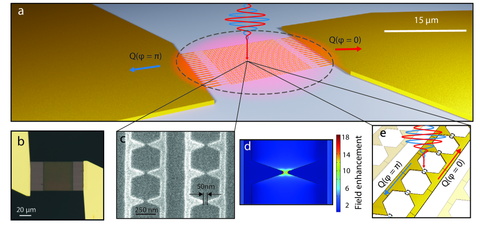
Our devices, as seen in Fig. 1 a, consist of 722 interconnected metallic (Au) bow-tie nanoantennas embedded in a by network. The device is integrated into a macroscopic circuit, allowing for charge readout with conventional electronics. The individual bow-tie nanoantennas, as shown in the scanning electron microscope image in Fig. 1 c, have designed dimensions of in length, in width and in thickness, resulting in an antenna density of . Fig. 1 d shows the finite element electromagnetic simulation of the field distribution, showing a peak enhancement of 8.2-fold for ( wavelength) localized at the tips of the bow-tie structure. This creates a spatially-confined hot spot for electron emission to occur. When the whole network is illuminated with a few-cycle infrared laser pulse with a peak electric field on the order of , highly nonlinear tunnel ionization of electrons occurs at these hotspots at the tip of the bow-tie antennas. Additionally, the tunnel ionization is temporally confined to the peak regions of the strongest half-cycles of the exciting field.
In the case of sufficiently strong electric fields, with a Keldysh parameter the tunneling emission for a metal-vacuum boundary is described by the quasi-static Fowler-Nordheim tunneling rate [27, 28, 29, 30], with noting the Heaviside function, the characteristic tunneling field strength for gold and a material and geometry dependent scaling factor. Since a single bow-tie is, in fact, a symmetric system consisting of two metal surfaces facing each other with a vacuum gap, we can approximate the total instantaneous currents at the junction with , as experimentally shown in [12, 21, 19]. A CW laser would lead to fully symmetric charge injection and transport across the gap. In this case, the time average of the residual charge in the network is zero. For the case of a few- to single-cycle pulse, however, the highly nonlinear dependence of the tunnel emission with respect to the electric field amplitude does generate a residual net charge. This is caused by the significant amplitude differences between the individual half-cycles of the pulse, effectively breaking the symmetry of emission and transport. To understand the symmetry breaking, it is useful to look at the detailed instantaneous tunneling rates as a function of the electric fields for a metal-vacuum boundary.
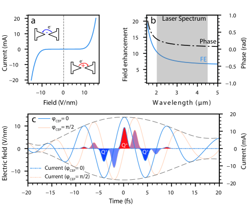
The instantaneous response of this system, shown in Fig. 2 a, is equivalent to two parallel diodes in opposing directions. Emission rates are taken from [31] and use the antenna tip surface area of .
Regarding the electron emission process, the local field at the tip of the nanoantenna is relevant. Therefore, we need to consider the antenna’s complex transfer function [2]. The antenna is designed to be off-resonant for two main reasons; the first is to transfer the full bandwidth of the optical pulse to the antenna tip, as a sharp resonance would increase the local pulse duration and reduce the CEP-dependent charge yield drastically. The second reason is that the fabrication process is not fully uniform throughout the detector area, resulting in small spectral shifts of the antenna resonance [19]. When designed on-resonance, small variations will transfer to sharp phase differences between individual antennas, as the phase response has a sharp jump at resonance. Therefore, when the antennas are driven off-resonance, small variations in the fabrication will not translate into sharp phase changes of the optical field at the antenna tip. The local field enhancement and the phase response of an off-resonance antenna for wavelengths above is shown in Fig. 2 b. The local field at the antenna tip is therefore the frequency domain multiplication of the incident pulse and the antennas complex frequency response , . The effective instantaneous current response of the system to such a pulse with a peak field of is shown in Fig. 2 c. The employed optical pulse shape is the reconstructed optical pulse used in the experimental apparatus, combined with the simulated local field enhancement (see Supplementary Sec. 2 and Sec 3.1 for details). The central half-cycle with the highest field amplitudes generates the largest peak current with up to for a duration of (FWHM). The neighboring half-cycles generate substantially smaller currents with the opposite sign. Since conventional electronics do not support the petahertz bandwidth currents, the device acts as an integrator, and the net charge deposited by the optical pulse resides in the circuit network, similar to a photodiode. The mathematical description of these charges as a function of the pulse CEP is simply the integral over the instantaneous currents;
| (1) | ||||
| (2) | ||||
| (3) |
The CEP dependence of the charge now stems from the small difference of and . For the case of a cosine pulse () the charge yield becomes maximal, and for the case of a sine pulse () the charge components cancel out to zero. Based on the results shown in [19] with 0.1 e per antenna, one can anticipate CEP-dependent charge amplitudes of around 1.4 e per antenna for the optical pulses used in our experiments and a peak field of . The resulting charge increase is due to a reduced number of cycles (from 2.5 to 2), and the use of a longer central wavelength [31]. With the known charge yield per antenna, one can extrapolate the charge yield of an array of interconnected antennas to a charge that is within the reach of reasonable detection limits.
Experiment and Results
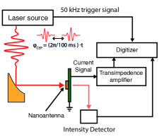
The optical pulses used in this work were generated with a home-built laser source based on optical parametric amplification and difference frequency generation that delivers passively CEP stable pulses with a FWHM duration down to at a center wavelength of . The pulse energy was at a repetition rate of . The CEP of the laser was controlled by adjusting the pump-seed delay in the difference frequency generation stage. This was implemented by controlling the pump beam path length via a retro-reflector mounted on a piezo-actuated linear stage. For a detailed description of the source, see the methods section A and Ref. [22].
To illuminate the nanoantenna network, we focused the incident pulse down to (FWHM) with an off-axis parabola of focal length . The nanoantenna arrays were placed in the center of the focus. For shot-to-shot charge readout, we used a custom transimpedance amplifier with a gain of and a -bandwidth of (WiredSense GmbH). The RMS noise of our detection was measured to be e per shot. To overcome this RMS noise floor, we illuminated a network consisting of 722 antennas in a rectangular area of by to generate in excess of 1000 e per shot.
After interaction with the nanoantenna arrays, pulse energies were measured by a pyroelectric photodetector with the same -bandwidth of as the transimpedance amplifier. This arrangement allowed for the simultaneous recording of shot-to-shot pulse energy fluctuations. The pyroelectric detector uses an identical transimpedance amplifier to the one used for the nanoantenna read-out to ensure comparable statistics of the two signals. More details on the acquisition and digitization of the signal are given in the Supplementary Information Sec. 3.1.
In this experiment, each dataset consists of the measured charge from the nannoantenna array and the corresponding pulse energy, recorded for around 50 000 shots (). In each dataset, the CEP of the laser is linearly ramped for with a speed of , starting at . For different datasets, the pulse energy was systematically varied by more than a factor of ten.
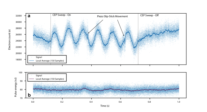
A single dataset is presented in Fig. 3, including both the single-shot data and the moving average calculated over 150 shots (dark line). The upper panel shows the recorded charge produced by the nanoantenna array, with an average yield of 25 000 e per shot. From to the CEP is linearly ramped over a range. The data points show a clear sinusoidal CEP dependence with an amplitude of 2370 e and an signal-to-noise ratio (SNR) of 4.6, while the pulse energy does not show modulation.
When considering the number of illuminated antennas, the individual CEP-sensitive yield per antenna and shot is 3.3 e, indicating peak currents through the nanoantenna gap of up to a 95 e/fs, corresponding to . Given the small cross-section of the nanoantenna tips, that is around , the current density reaches a remarkable .
At and , sharp changes are visible in the charge yield of the detector element. These features, which are apart, are caused by the specific movement pattern of the closed-loop slip-stick piezo stage used to control the CEP, that recenters the piezo position every .
To isolate the CEP-dependent signal from readout noise and pulse energy fluctuations, we Fourier transformed the dataset between and and compared it to the frequency spectrum obtained without any optical input; see Fig. 4.
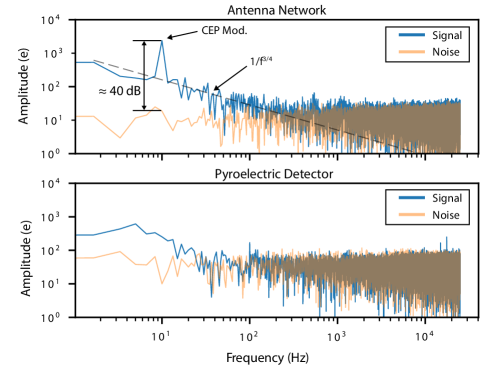
The spectrum of the antenna array shows a clear peak at corresponding to the modulation of the CEP. This signal is around two orders of magnitude higher than the readout noise floor (corresponding to ). The noise in the measured spectrum is dominated from DC to by scaling, which is typical for field emission devices and is attributed to Brownian noise of the work function due to dynamical changes of adsorbates on the surface [32, 19]. At frequencies higher than the spectrum is limited by shot noise, with a substantial component originating from the detection noise of the transimpedance amplifier itself. The calculated shot noise of the signal is e rms. When evaluating the recorded pulse energy fluctuations at the photodetector, no modulation is distinguishable from the background (see Fig. 4 b). Above the pulse energy spectrum is dominated by detector noise. Systematic investigation of signal strength as a function of peak electric field has shown that at resolution bandwidth a signal distinguishable from noise can be observed down to (corresponding to ). See Supplementary Sec. 4.1 for details.
Conclusion
We have demonstrated single-shot readout of CEP-dependent charge signals at repetition rate, underlying sub-cycle current generation across a macroscopic device area of integrating more than individual antenna pairs. This was made possible by improving the average CEP-dependent charge yield per single antenna by a factor of 30 [19, 21], now reaching 3.3 e per shot, and by illuminating hundreds of antennas simultaneously. The enhanced antenna yield implies a remarkable peak current density of up to [19, 12, 21]. With this result, we show that metallic nanoantenna networks, fabricated via state-of-the-art lithographic methods, are a flexible and scalable approach to optical frequency electronics that allows the designing of individual circuit elements, similar to conventional microelectronics. Thanks to this advance, we demonstrated off-resonant antennas that are sensitive to pulse energies two orders of magnitude lower than any other comparable single-shot absolute CEP detection technique [33, 23, 18], enabling CEP detection of optical pulses with only tens of nanojoules of energy. Further optimization of the network density (see supplementary Sec. S2) combined with a reduced number of optical cycles in the pulse would potentially increase the total yield by an additional two orders of magnitude [31, 19]. As the measurement is dominated by read-out noise, further noise reduction of electronics downstream of the detector element will have a significant impact on SNR with potential for another 5-fold improvement [34].
Given the exceptional current densities generated in these nanometer-sized devices, further studies will be necessary to elucidate the role of electron-electron interaction during the sub-cycle emission process [35]. Based on this platform, many different experiments and applications can be developed, such as the investigation of petahertz bandwidth logic gates and memory cells [3, 14]. The extremely small device size, comparable to the pixel size in modern Si-based CMOS detectors, combined with the reduced pulse energy requirements, enables the integration of multiple nanoantenna arrays in a larger pixel matrix. This will allow for a CEP-sensitive camera with further improved noise performance [36]. Absolute single-shot CEP tagging can also be implemented by adapting I/Q demodulation with two separate networks recording phase-shifted currents. The previously demonstrated techniques of attosecond-resolved field sampling can be extended to single-shot readout, by making large line arrays of individual networks [2, 37]. Another area of progress will be the adaptation of the fabrication process to become fully CMOS-compatible by replacing gold with aluminum or copper. With our results and natural avenues of progress, we believe that our platform will play a major role in future electronics operating at optical frequencies.
Appendix A Methods
Laser source
The two-cycle MIR source used to illuminate the nanoantenna networks is a home-built system based on adiabatic difference frequency generation (DFG) [38] and details can be found in [22]. The setup is based on a commercial Yb:KYW regenerative amplifier with a center wavelength of , a pulse duration of , delivering up to at a repetition rate of . The first stage of the optical setup consists of a non-collinear optical parametric amplifier seeded with white light and pumped by the second harmonic of the pump laser [39]. The amplified seed has an energy of approximately at a center wavelength of . After the amplification, the seed is stretched for pre-compensation of the later acquired MIR dispersion, and the pulse energy is controlled by an anti-reflection coated metallic neutral density filter wheel. For generation of the passively CEP stable DFG output in the MIR, the amplified seed and the stretched pump laser of propagate collinear through an adiabatically poled Mg:LiNbO3 crystal with an identical design to Krogen et al. [38]. The generated broadband MIR pulse covers the spectral range of to at an energy of up to and is compressed through dispersion in BaF2 and silicon. The generated pulse has a duration down to (FWHM) at a center wavelength of , characterized by a two-dimensional spectral shearing interferometry setup. The passive CEP stability of the MIR pulse inherent to the difference frequency generation process is measured with an f-2f interferometer to rms over .
Nanofabrication
A fused silica wafer was purchased from MTI Corporation and cut with a die saw. The substrates were cleaned by sonicating in acetone and isopropyl alcohol for 5 minutes each. Subsequently, the pieces were cleaned using an oxygen plasma. Poly(methyl methacrylate) A2 was spun at 2,500 revolutions per minute and baked at , then DisCharge H2O (DisChem Inc.) was spun at 1,000 revolutions per minute so that charging did not occur during the electron beam lithography write.
Electron beam lithography was performed using an electron beam energy of 125 keV with doses varied from 4000-6000 C cm2 with a proximity effect correction. After exposure, the resist was developed in a 3:1 isopropyl alcohol/methyl isobutyl ketone solution for 50 seconds at . Subsequently, the antenna deposition was performed using an electron beam evaporator operating below Torr. First, a 2 nm adhesion layer was deposited, then 20 nm of gold. Lift-off was performed in a - bath of N-methylpyrrolidone.
After antenna fabrication, contacts were patterned by photolithography using a bilayer of PMGI and S1838 both spun at 4,500 revolutions per minute. The deposition was performed by electron beam evaporation with a adhesion layer and of gold so that they could be wire-bonded to a printed circuit board.
Appendix B Extended Data Figures
Data Availability
All data is available under reasonable request to the authors.
Code Availability
All code is available under reasonable request to the authors.
Acknowledgements
We thank John Simonaitis and Stewart Koppell for their assistance in reviewing the manuscript. The authors F. Ritzkowsky and P.D. Keathley thank William Putnam for many insightful scientific discussions on the experiments. H. Cankaya and F. Ritzkowsky thank Haim Suchowski for designing the ADFG crystal used for this work. F. Ritzkowsky and M. Yeung thank Marco Turchetti for his contributions to the sample fabrication process. M. Budden and T. Gebert thank Johannes Kunsch and Laser Components Germany GmbH for the support in the development of pyroelectric sensor elements specifically tailored to this high-speed application. F. Ritzkowsky and all authors affiliated with Deutsches Elektronen-Synchrotron (DESY) thank the administrative and engineering support staff at DESY for assisting with this research. We acknowledge the use of a PIER Hamburg grant for supporting M. Yeung to travel to DESY to set up initial measurements.
F.X. Kärtner and F. Ritzkowsky acknowledge funding by: European Union’s Seventh Framework programme 145 (FP7/2007-2013) ERC Synergy Grant ‘Frontiers in Attosecond X-ray Science: Imaging and Spectroscopy’ (AXSIS) (609920); Cluster of Excellence ‘CUI: Advanced Imaging of Matter’ of the Deutsche Forschungsgemeinschaft (DFG)—EXC 2056—project ID 390715994; Deutsche Forschungs Gemeinschaft (DFG)— project ID KA908/12-1 and project ID 453615464.
This research is supported by the Air Force Office of Scientific Research (AFOSR) grant under contract NO. FA9550-18-1-0436. M. Yeung acknowledges support from the National Science Foundation Graduate Research Fellowship Program, Grant No. 1745302
Author Contributions
FR, MY, FK and PK conceived the experiments. The samples were fabricated by MY with guidance from PK and KB. The experimental setup was constructed by FR with assistance from EB, GR, RM, and HC. The readout electronics were set up by FR, TG, MB and TM. The data was taken by FR. The data was analyzed by FR with input from MY and PK. The electromagnetic simulations were done by EB with input from FR, MY and PK. The manuscript was written by FR with significant contributions from MY, PK, GR and editing from all authors.
Competing Interests
The authors declare no conflict of interest.
References
- [1] Ferenc Krausz and Mark I. Stockman “Attosecond metrology: from electron capture to future signal processing” Number: 3 In Nature Photonics 8.3, 2014, pp. 205–213 DOI: 10.1038/nphoton.2014.28
- [2] Mina R. Bionta et al. “On-chip sampling of optical fields with attosecond resolution” In Nature Photonics 15.6, 2021, pp. 456–460 DOI: 10.1038/s41566-021-00792-0
- [3] Tobias Boolakee et al. “Light-field control of real and virtual charge carriers” Number: 7909 Publisher: Nature Publishing Group In Nature 605.7909, 2022, pp. 251–255 DOI: 10.1038/s41586-022-04565-9
- [4] John Ambrose Fleming “On the conversion of electric oscillations into continuous currents by means of a vacuum valve.” In Proceedings of the Royal Society of London 74.497-506, 1905, pp. 476–487 DOI: 10.1098/rspl.1904.0143
- [5] Michael Krüger, Markus Schenk and Peter Hommelhoff “Attosecond control of electrons emitted from a nanoscale metal tip” Number: 7354 In Nature 475.7354, 2011, pp. 78–81 DOI: 10.1038/nature10196
- [6] H.. Kim et al. “Attosecond field emission” Number: 7945 Publisher: Nature Publishing Group In Nature 613.7945, 2023, pp. 662–666 DOI: 10.1038/s41586-022-05577-1
- [7] Philip Dienstbier et al. “Tracing attosecond electron emission from a nanometric metal tip” Number: 7958 Publisher: Nature Publishing Group In Nature 616.7958, 2023, pp. 702–706 DOI: 10.1038/s41586-023-05839-6
- [8] Martin Schultze et al. “Controlling dielectrics with the electric field of light” In Nature 493.7430, 2013, pp. 75–78 DOI: 10.1038/nature11720
- [9] Agustin Schiffrin et al. “Optical-field-induced current in dielectrics” Number: 7430 Publisher: Nature Publishing Group In Nature 493.7430, 2013, pp. 70–74 DOI: 10.1038/nature11567
- [10] Shawn Sederberg et al. “Vectorized optoelectronic control and metrology in a semiconductor” Number: 11 Publisher: Nature Publishing Group In Nature Photonics 14.11, 2020, pp. 680–685 DOI: 10.1038/s41566-020-0690-1
- [11] Takuya Higuchi et al. “Light-field-driven currents in graphene” Number: 7675 Publisher: Nature Publishing Group In Nature 550.7675, 2017, pp. 224–228 DOI: 10.1038/nature23900
- [12] Tobias Rybka et al. “Sub-cycle optical phase control of nanotunnelling in the single-electron regime” In Nature Photonics 10.10, 2016, pp. 667–670 DOI: 10.1038/nphoton.2016.174
- [13] William P. Putnam et al. “Optical-field-controlled photoemission from plasmonic nanoparticles” Number: 4 In Nature Physics 13.4, 2017, pp. 335–339 DOI: 10.1038/nphys3978
- [14] J.. Lee, Youngjae Kim and Chil-Min Kim “Model for petahertz optical memory based on a manipulation of the optical-field-induced current in dielectrics” Number: 9 Publisher: IOP Publishing In New Journal of Physics 20.9, 2018, pp. 093029 DOI: 10.1088/1367-2630/aae100
- [15] Seung Beom Park et al. “Direct sampling of a light wave in air” Number: 4 In Optica 5.4, 2018, pp. 402–408 DOI: 10.1364/OPTICA.5.000402
- [16] Dmitry Zimin et al. “Petahertz-scale nonlinear photoconductive sampling in air” Publisher: Optica Publishing Group In Optica 8.5, 2021, pp. 586–590 DOI: 10.1364/OPTICA.411434
- [17] Dandan Hui et al. “Attosecond electron motion control in dielectric” Number: 1 Publisher: Nature Publishing Group In Nature Photonics 16.1, 2022, pp. 33–37 DOI: 10.1038/s41566-021-00918-4
- [18] M. Kubullek et al. “Single-shot carrier–envelope-phase measurement in ambient air” Number: 1 Publisher: Optica Publishing Group In Optica 7.1, 2020, pp. 35–39 DOI: 10.1364/OPTICA.7.000035
- [19] Yujia Yang et al. “Light phase detection with on-chip petahertz electronic networks” In Nature Communications 11.1, 2020, pp. 3407 DOI: 10.1038/s41467-020-17250-0
- [20] P.. Keathley et al. “Vanishing carrier-envelope-phase-sensitive response in optical-field photoemission from plasmonic nanoantennas” In Nature Physics, 2019, pp. 1–6 DOI: 10.1038/s41567-019-0613-6
- [21] Markus Ludwig et al. “Sub-femtosecond electron transport in a nanoscale gap” Number: 3 Publisher: Nature Publishing Group In Nature Physics 16.3, 2020, pp. 341–345 DOI: 10.1038/s41567-019-0745-8
- [22] Felix Ritzkowsky et al. “Passively CEP stable sub-2-cycle source in the mid-infrared by adiabatic difference frequency generation” Publisher: Optica Publishing Group In Optics Letters, 2023 DOI: 10.1364/OL.485610
- [23] Dominik Hoff et al. “Continuous every-single-shot carrier-envelope phase measurement and control at 100 kHz” Publisher: Optica Publishing Group In Optics Letters 43.16, 2018, pp. 3850–3853 DOI: 10.1364/OL.43.003850
- [24] I.. Sola et al. “Controlling attosecond electron dynamics by phase-stabilized polarization gating” Number: 5 Publisher: Nature Publishing Group In Nature Physics 2.5, 2006, pp. 319–322 DOI: 10.1038/nphys281
- [25] G. Sansone et al. “Isolated Single-Cycle Attosecond Pulses” Publisher: American Association for the Advancement of Science In Science 314.5798, 2006, pp. 443–446 DOI: 10.1126/science.1132838
- [26] Giulio Maria Rossi et al. “Sub-cycle millijoule-level parametric waveform synthesizer for attosecond science” In Nature Photonics 14.10, 2020, pp. 629–635 DOI: 10.1038/s41566-020-0659-0
- [27] L.. Keldysh “Ionization in the Field of a Strong Electromagnetic Wave” Number: 5 In Sov. Phys. JETP 20.5, 1965, pp. 1307–1314
- [28] F V Bunkin and M V Fedorov “Cold Emission of Electrons from Surface of a Metal in a Strong Radiation Field” Number: 5 ISBN: 0038-5646 In Soviet Physics JETP 21.5, 1965, pp. 896–899
- [29] R.. Fowler and L. Nordheim “Electron Emission in Intense Electric Fields” In Royal Society of London Proceedings Series A 119, 1928, pp. 173–181 DOI: 10.1098/rspa.1928.0091
- [30] Gennady L. Yudin and Misha Yu. Ivanov “Nonadiabatic tunnel ionization: Looking inside a laser cycle” Number: 1 In Physical Review A 64.1, 2001, pp. 013409 DOI: 10.1103/PhysRevA.64.013409
- [31] Drew Buckley et al. “Nanoantenna design for enhanced carrier–envelope-phase sensitivity” Number: 9 Publisher: Optica Publishing Group In JOSA B 38.9, 2021, pp. C11–C21 DOI: 10.1364/JOSAB.424549
- [32] G.. Timm and A. Van der Ziel “Noise in field emission diodes” In Physica 32.7, 1966, pp. 1333–1344 DOI: 10.1016/0031-8914(66)90125-X
- [33] T. Wittmann et al. “Single-shot carrier–envelope phase measurement of few-cycle laser pulses” Number: 5 Publisher: Nature Publishing Group In Nature Physics 5.5, 2009, pp. 357–362 DOI: 10.1038/nphys1250
- [34] M. Andrä et al. “Towards MYTHEN III - prototype characterisation of MYTHEN III.0.2” In Journal of Instrumentation 14.11, 2019, pp. C11028 DOI: 10.1088/1748-0221/14/11/C11028
- [35] Johannes Schötz et al. “Onset of charge interaction in strong-field photoemission from nanometric needle tips” Publisher: De Gruyter In Nanophotonics 10.14, 2021, pp. 3769–3775 DOI: 10.1515/nanoph-2021-0276
- [36] Jiaju Ma, Saleh Masoodian, Dakota A. Starkey and Eric R. Fossum “Photon-number-resolving megapixel image sensor at room temperature without avalanche gain” Publisher: Optica Publishing Group In Optica 4.12, 2017, pp. 1474–1481 DOI: 10.1364/OPTICA.4.001474
- [37] Yangyang Liu et al. “Single-shot measurement of few-cycle optical waveforms on a chip” Number: 2 Publisher: Nature Publishing Group In Nature Photonics 16.2, 2022, pp. 109–112 DOI: 10.1038/s41566-021-00924-6
- [38] Peter Krogen et al. “Generation and multi-octave shaping of mid-infrared intense single-cycle pulses” In Nature Photonics 11.4, 2017, pp. 222–226 DOI: 10.1038/nphoton.2017.34
- [39] C. Manzoni and G. Cerullo “Design criteria for ultrafast optical parametric amplifiers” In Journal of Optics 18.10, 2016, pp. 103501 DOI: 10.1088/2040-8978/18/10/103501