Bandgap manipulation of hBN by alloying with aluminum: absorption properties of hexagonal BAlN
Abstract
The versatile range of applications for two-dimensional (2D) materials has encouraged scientists to further engineer the properties of these materials. This is often accomplished by stacking layered materials into more complex van der Waals heterostructures. A much less popular but technologically promising approach is the alloying of 2D materials with different element compositions. In this work, we demonstrate a first step in manipulating the hBN bandgap in terms of its width and indirect/direct character of the optical transitions. We present a set of aluminum alloyed hexagonal boron nitride (hBAlN) samples that were grown by metal organic vapor phase epitaxy (MOVPE) on 2-inch sapphire substrates with different aluminum concentration. Importantly, the obtained samples revealed a sp2-bonded crystal structure. Optical absorption experiments disclosed two strong peaks in the excitonic spectral range with absorption coefficient cm-1. Their energies correspond very well with the energies of indirect and direct bandgap transitions in hBN. However, they are slightly redshifted. This observation is in agreement with predictions that alloying with Al leads to a decrease of the bandgap energy. The observation of two absorption peaks can be explained in terms of mixing electronic states in the K and M conduction band valleys, which leads to a significant enhancement of the absorption coefficient for indirect transitions.
I INTRODUCTION
The initial research on graphene has motivated researchers to explore the properties of other atomically thin layered materials (2D materials) and their stacks, sometimes referred to as NanoLego structures [1, 2, 3, 4]. This is typically accomplished by stacking different layers together into into van der Waals heterostructures [5, 6]. Combining these materials using epitaxial growth provides the additional opportunity to scale-up such structures or to create new ones by growing materials as alloys with appropriate composition [7, 8]. In the case of hexagonal boron nitride (hBN), the natural choice is alloying hBN with aluminum and gallium, since they are in the same group of the periodic table as boron. Research on the novel hB1-x-yAlxGayN material (where and stand for Al and Ga concentration in the alloy respectively) is interesting in terms of exploration of new physical phenomena as well as form a technological point of view. hBN with its, unusual for III-N, strong sp2 covalent bonds in plane and weak van der Waals bonds out of plane exhibits extraordinary properties [9]. One of the intriguing facts is that inspite of the indirect character of the bandgap, hBN shows a photoluminescence (PL) emission intensity of the band-edge transition as strong as for direct semiconductors [10]. Thus, the possibility of tuning the hBN bandgap using Al opens up further prospects for applications in hBN-based quantum wells and optoelectronic devices. The same scheme could be used for hBN alloying with Ga. Tunable hBAlN, hBGaN or hBAlGaN alloys could become promising candidates for building blocks of efficient light sources in the deep UV spectral range (DUV, 200-280 nm, 4.4-6.2 eV). Such candidates are of high importance, since nowadays the efficiency of semiconductor light sources operating in DUV is very limited (10% for 270-280 nm and 3% for 250 nm) [11]. This spectral range is crucial, for example for the disinfection and sterilization of air, water and surfaces [12, 13].
However, before hBN-based quantum structures and DUV light sources can be realized, more fundamental questions must be answered. Firstly, it is still unclear how to tune the hBN bandgap energy. This knowledge would be of great importance for designing hBN-based quantum wells that would trap carriers and enhance emission from the structure. Moreover, it would be very beneficial for further improvement if one could change the nature of the hBN bandgap from indirect to direct [14, 15].
In this work, we present results for boron nitride layers grown by metal organic vapor phase epitaxy (MOVPE) that were alloyed with aluminum. We obtained materials that preserve a sp2-bonded crystal structure. The produced hB1-xAlxN layers with aluminum concentration up to a few percent exhibit strong absorption for two energies that coincide with energies of indirect and direct bandgap in hBN. Our approach that uses MOVPE to grow this novel material provides a perspective for further development of the hBAlN alloy composition control in terms of doping for conductivity, manipulation of the bandgap, and commercial up-scaling.
II METHODS
II.1 Samples
The samples used in these studies were grown using an Aixtron CCS 32” metal organic vapor phase epitaxy system. The growth was carried out on 2-inch sapphire -plane substrates with 0.3∘ off-cut. For the growth of layered sp2-bonded hB1-xAlxN samples ammonia, triethylboron (TEB) and trimethylaluminum (TMAl) were used as nitrogen, boron, and aluminum precursors, respectively and hydrogen was used as a carrier gas. Note that we used the hBAlN notation (with letter h) to highlight the importance of the hexagonal hBN-like crystal structure of the obtained material. The precursors were injected alternatively following the flow modulation epitaxy growth mode [16]. The scheme of pulses in a single cycle was as follows: TEB-NH3-TMAl-NH3. The growth temperature was kept at 1300 ∘C. The temperature value was obtained with an in situ multipoint optical pyrometer (ARGUS). NH3 and TEB flows were fixed for all samples (V/III ratio for TEB-NH3 pulses was ). The TMAl/III ratio (III = TEB + TMAl) in the process varied for the samples: (ratio 0.02), (ratio 0.04), (ratio 0.07), (ratio 0.13). Such a ratio (TMAl/III) gives an insight into relation between B and Al source in a gas phase during the process and very initial predictions of the material composition . To obtain the lowest ratio, the duration of consecutive pulses of TMAl and NH3 was reduced by half. This step was enforced by the minimal precursor flow limitation in our system. The number of pulsing cycles was chosen in such a way that all samples were grown 60 minutes.
II.2 Experimental details
The crystal structure of the samples was examined with a Panalytical X’Pert diffractometer with standard CuKα x-ray source. The x-ray light beam was formed by an x-ray mirror for Bragg-Brentano optics. Infrared reflectance spectra were collected with a Thermo Scientific Nicolet Continuum Infrared Microscope equipped with a 32x Schwarzschild infinity corrected objective (NA 0.65). All samples of mm were measured with a perpendicular incident beam on five m areas placed in the center and four corners of the sample. Spectra were collected in the range of 650-4000 cm-1 with a resolution of 0.482 cm-1. The surface morphology was examined by scanning electron microscopy (SEM) using a FEI Helios NanoLab 600 system. Absorption spectra were measured using a Varian Cary 5000 UV-vis-NIR spectrophotometer in dual-beam mode with nitrogen purging. The spectral bandwidth was set to 1 nm.
III RESULTS
III.1 x-ray diffraction
In figure 1a) we present x-ray diffraction scans collected for all the studied samples. The peaks at , and correspond to the 0003 and 0006 planes of Al2O3. In figures 1b), c) we present a zoom on the peaks at and that come from the reflection of the 0002 planes in sp2-BAlN and sp3-AlN. The parameters of the Gaussian curve fit performed on the data concerning hBAlN are included in table 1. Note that the 0002 BAlN peak related to sample is asymmetric, so we fitted two Gaussian curves yielding two different components of the peak. The components originate from turbostratic (tBAlN, lower angles) and hexagonal (hBAlN, higher angles) phases of sp2-bonded BAlN [17, 19]. In the further analysis we will focus only on the hexagonal phase. In table 1 we do not observe significant changes in the peak position and the full width at half maximum (FWHM) for the hBAlN peak. This implies that the lattice constant is comparable for all the samples ( Å) as well as the thickness of the crystal. The only monotonous trend can be found in the amplitude of the hBAlN peak. This means that the misorientation of the 0002 crystal planes is enlarged when increasing the TMAl flow.
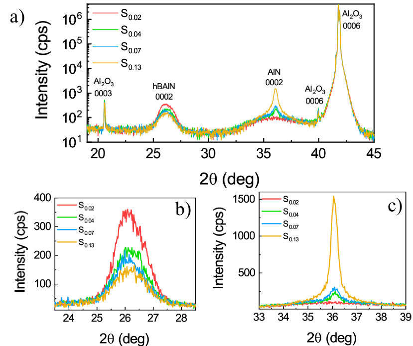
| Sample | amplitude (cps) | 2 (deg) | FWHM (deg) |
|---|---|---|---|
| 7.0(6) | 25.84(1) | 0.51(4) | |
| 28.2(5) | 26.187(9) | 1.28(1) | |
| 18.5(2) | 26.136(6) | 1.29(1) | |
| 15.0(2) | 26.078(7) | 1.31(2) | |
| 11.4(2) | 26.122(8) | 1.36(2) |
The signal associated to AlN consists of a very broad peak, which is alike for all the samples and a narrower component that changes its intensity. In fact, these two components have different origins. The broad component comes from an unintentional thin (2 nm) AlN layer that is created on the hBAlN-sapphire interface during the initial growth stage. This kind of layer is characteristic for MOVPE-grown hBN [19, 20]. However, in accordance with the enhancement of the sharp component with an increase in TMAl, we can deduce the formation of AlN crystals in our samples. These crystals do not seem to influence the crystal structure of hBAlN as we do not observe any correlation between the intensity of the sharp peak at and the values of and FWHM in table 1 which are related to BAlN.
III.2 Fourier-transform infrared spectroscopy
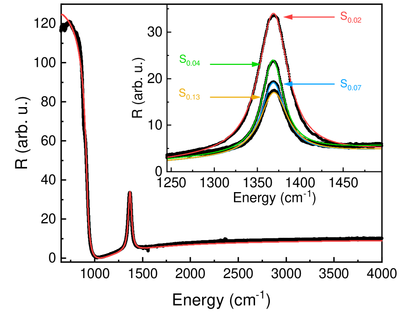
In figure 2 we present exemplary infrared reflectance spectra obtained for the studied samples. The peak observed about 1368 cm-1 is related to the vibrational mode characteristic for hBN [21]. The observation of this peak provides direct evidence that our samples are sp2 bonded. The high reflectance below 1000 cm-1 comes from the sapphire substrate. Barely visible small and sharp peaks about 1550 cm-1, 2300 cm-1 and 3500 cm-1 correspond to transitions in the atmospheric gases present during the experiment.
To make the FTIR results quantitative, we implemented a spectra analysis method, as described in the Ref. [22]. In this method, it is assumed that the material is composed of harmonic oscillators with self-energy and damping parameter . It makes use of the Dynamic Dielectric Function (DDF) of the materials in the structure (boron nitride and sapphire in this case). The substantial advantage of this method is the possibility of characterizing the grown layer itself. The self-energy of the oscillator (phonon energy, peak position), its damping parameter (peak broadening) and layer thickness provide information about strain, homogeneity and growth rate. In table 2 we present the best fit parameters obtained as an average of 5 points measured for each sample.
| Sample | (cm-1) | (cm-1) | (nm) |
|---|---|---|---|
| 1368.94(5) | 24.5(1) | 18.6(5) | |
| 1368.03(3) | 22.1(2) | 9.1(4) | |
| 1368.7(2) | 26.5(6) | 9.8(3) | |
| 1369.3(2) | 30.1(5) | 10.1(3) |
The fitted parameters are monotonous for the samples , and . The increase in TMAl flow leads to an increase in phonon energy and peak broadening, which suggest the introduction of an inhomogeneous compressive strain within the layer. The changes of (0.63 cm-1 for the following samples) and (4 cm-1 for the following samples) are significant in terms of FTIR measurements. Remarkably different is the trend for the layer thickness. The 4-time increase in amount of TMAl (samples and ) resulted in a layer that is only 1 nm thicker, which is equivalent to the increase of the growth rate by less than 0.02 nm/min.
The sample clearly stands out and does not follow the same trends. The reason for this behavior is most likely due to the change of TMAl-NH3 pulse duration necessary to obtain a TMAl/III ratio equal to 0.02. This led to a double increase in growth rate compared to the sample . This result is reasonable, since the TMAl/III ratio for was twice higher than for . At the same time the number of TEB pulses increased by 33%. So we find the competition between TEB-NH3 and TMAl-NH3 pulses to be more important for the growth rate rather than the change in number of TEB pulses in the growth process.
III.3 scanning electron microscopy
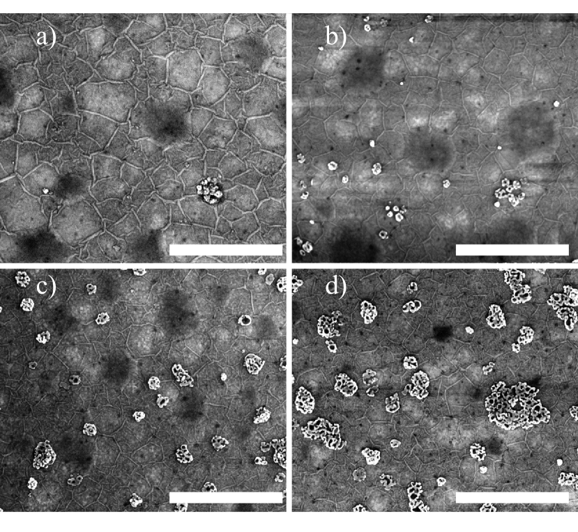
The morphology of the studied samples is presented in figure 3. For each sample, a characteristic wrinkle pattern is observed. The wrinkles are created during cooling down the material after the growth process and are due to the relaxation of strain caused by the difference in thermal expansion coefficients of the layer and the substrate [22]. Because of the mechanism of the wrinkle formation their presence is an evidence for the continuity of the hBAlN epitaxial layer. The wrinkles are most pronounced for sample , which is due to a much larger thickness. The darker circular areas in the images are bubbles with hydrogen inside. They are created during SEM imaging and are the result of the radiolysis of interfacial water via electron irradiation [23]. The size of crystalline objects on the surface of the layer is correlated with the amount of TMAl present in the process. This observation is in good agreement with the XRD results for which the AlN narrow diffraction peak was observed for , and . This leads to the conclusion that the observed crystals are related to sp3 bonded aluminum nitride. More detailed atomic force microscopy and Raman spectroscopy studies of these objects are presented in the Supplementary Materials.
III.4 UV-vis spectroscopy
To extract the absorption coefficient from the measured absorbance, we subtracted the absorbance spectrum obtained for bare sapphire. To calculate the absorption coefficient we used the thickness of the layer taken from table 2. The absorption coefficient spectra of the samples studied are presented in figure 4. The spectrum for the reference epitaxial boron nitride without aluminum sample was obtained in the same way. The reference sample was grown analogously to the sample presented in the work in Ref. [17]. The absorption coefficient for all the samples is of order of cm-1. This value is twice higher as compared to those previously reported for boron nitride [9, 24, 25]. In contrast to the reference sample, the samples with aluminum exhibit two well-resolved peaks. In previous studies only peak shifting was observed, which was accompanied by a broadening due to a decrease of sample quality [26]. In the case of our samples the two peak energies are close to the dash-dotted navy and dashed green lines that are positioned at energies corresponding to the indirect (5.955 eV [27]) and direct (6.125 eV [28, 29]) band-edge transitions in boron nitride, respectively. Depending on the TMAl flow, one can change the intensity of those peaks and the intensity ratio between higher and lower energetic peaks. However, this relationship does not correlate with the amount of TMAl in the growth process.
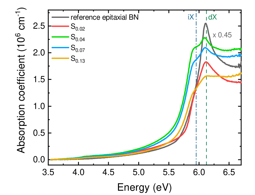
The lower energy peak, which is not observed for the reference sample, could be thought to be the result of the crystaline objects presented in the SEM images (figure 3). However, the peak intensity does not scale with the number of objects on the layer’s surface. Secondly, as has been mentioned before, the crystalities are identified as sp3 bonded AlN which is known to have a bandgap energy of 6.2 eV [30]. Possible alloying of sp3 bonded wurtzite-AlN (wAlN) with boron would, on the other hand, further increase the bandgap since wurtzite-BN (wBN) is a wider bandgap semiconductor [14]. Consequently, the signal coming from AlN should be observed in the absorption spectra for higher, not lower energies when comparing to the peak of pure boron nitride. However, we cannot provide conclusive information about the AlN-related spectral component since this energy range is close to the limit of detection for our spectrometer.
IV DISCUSSION
As presented in figure 1b) and table 1, the x-ray diffraction peak is observed at angles lower than expected for the 0002 hBN plane (26.764∘ [31]). This indicates a larger lattice constant in the direction. However, the peak position does not change significantly between the samples, which is in contrast to the results reported in Ref. [32] in which authors observed peak position shifting towards higher angles with an increasing TMAl flow. According to theoretical DFT calculations presented in Ref. [33], a decrease in the lattice constant should be observed when hBN is alloyed with Al, since hexagonal aluminum nitride has calculated a smaller lattice constant. We conclude that since we do not have a perfect hexagonal phase the main reason for the XRD peak position change in our samples is that it is attributed to random twists of subsequent atomic layers, which make the material more turbostratic. In this case we postulate that the peak position variations related to the alloying with small amounts of Al are just a higher order correction. This hypothesis seems to be confirmed by the fact that all samples were grown under the same growth conditions. Another prominent feature presented in figure 1c) is the peak at , whose intensity increases with the increase in TMAl flow. The value of the peak position is in agreement with the XRD peak of 0002 AlN in the crystal structure of wurtzite [34]. This indicates the creation of sp3 bonded wAlN crystals, which scale with the amount of TMAl. This additional notable peak is a proof of the phase separation of sp2 bonded hBAlN and sp3 bonded wAlN. The observation agrees with SEM (figure 3), Raman spectroscopy and AFM (Supplementary Materials) measurements. Indeed, the number and size of crystaline objects correlate with the amount of TMAl, which provides strong evidence for the very limited solubility of aluminum in the hexagonal boron nitride layer at the temperature and pressure used in the growth process (1300 ∘C, 400 mbar). Consequently, the experimental determination of the material composition is very difficult and needs further studies. Standard composition-determination techniques such as energy-dispersive x-ray spectroscopy (EDS), x-ray photoelectron spectroscopy (XPS), secondary ion mass spectroscopy (SIMS) cannot be employed to correctly determine the composition. Because the analyzed material is dielectric, electron charging is significant and does not allow EDS to be measured in one area for a longer period of time. Additionally, due to the electrons penetration depth in EDS it is hard to differentiate signal for Al that comes from the hBAlN layer and Al2O3 substrate. XPS and SIMS hardly distinguish Al from the hBAlN layer and AlN crystalities on its surface.
Although AlN crystalines can be observed, the sp2-bonded, layered structure of hBAlN is maintained, which is proved by FTIR measurement presented in figure 2. However, by introducing TMAl we modify the optical properties of the layer. This can be seen as a shift of the phonon energy towards higher energies that suggests compressive stress in the structure as demonstrated in Ref. [35]. Furthermore, the increase in TMAl is followed by a broadening of the peak described by the parameter , which indicates a defect-related inhomogeneity of the strain within the layer.
The most striking result that emerges from our work is the observation of an additional low energy peak in the absorption spectra. The hBN conduction band is known to consist of minima at the K and M points of the Brillouin zone that are energetically close to each other [10]. They are responsible for direct and indirect band transitions, respectively. As an indirect transition is a three-particle (photon, electron, phonon) event, it has a much lower probability to occur than a direct transition, which requires only two particles (photon, electron). Consequently, the absorption coefficient related to indirect transitions is usually 2-3 orders of magnitude lower as compared to direct ones. However, in the case of our samples, we observe two peaks at energies which coincide with the energies of direct and indirect transitions in hBN (dash-dotted and dashed lines in figure 4). Furthermore, both have a very high value of the absorption coefficient ( cm-1) typical for direct bandgap transitions. Notably that the lower-energy peak has even lower energy than expected for the indirect transition in hBN. This observation is in agreement with predictions about a decrease in bandgap energy when hBN is alloyed with Al [36]. To understand the mechanism that stands behind the observation of the two peaks in the absorption spectra, we need to be aware of the role of aluminum in the crystal structure. Al incorporation introduces short range disorder, which in turn would lead to the mixing of states with large -vectors. As presented in Ref. [10], conduction and valence bands along KH and ML points in hBN are very flat and almost parallel to each other. This feature leads to high oscillator strength and consequently very efficient absorption. A disorder induced by Al incorporation further modifies the band structures and the probability of electronic transitions, i.e. oscillator strength. Consequently, other absorption channels are enabled through the defect-related states. The modification of states caused by Al-related defects allows us to observe highly effective absorption for both energies. However, further increase of TMAl flow and limited solubility of Al in hBN lead to a deterioration of optical quality of the material which is observed in broadening of spectroscopic peaks in the spectra (same for FTIR and UV-Vis).
V CONCLUSIONS
In this work, we have shown the results for MOVPE grown hB1-xAlxN layers with TMAl/III ratio ranging from 0.02 to 0.13. X-ray diffraction and Fourier-transform infrared spectroscopy measurements proved that the obtained material maintained a sp2-bonded layered crystal structure, which is characteristic for hBN. At this stage of the research, we are faced with a challenge of insufficient information regarding the exact composition of the material, as well as the presence of crystaline sp3-bonded AlN clusters on the surface of the material. However, despite these obstacles, we managed to observe a significant change in the layer properties. Most importantly, we have shown two peaks of strong absorption ( cm-1) typical for direct excitonic transitions in hBN. The peak energies coincide with the energy of the indirect and direct bandgap transition in hBN. This observation becomes possible due to an activation of the absorption channels through defects caused by Al incorporation. The presented results are of great importance to understand how the boron nitride bandgap can effectively be manipulated in terms of its indirect/direct nature and its width. Understanding these processes is a key aspect for the fabrication of hBN-based structures for efficient deep UV emission.
Acknowledgements.
This work was supported by the National Science Centre, Poland, under the decisions 2019/33/B/ST5/02766, 2020/39/D/ST7/02811 and 2022/45/N/ST5/03396.References
- [1] Novoselov KS, Geim AK, Morozov SV, Jiang De, Zhang Y, Dubonos SV, et al. Electric field effect in atomically thin carbon films. science. 2004;306(5696):666-9.
- [2] Novoselov KS, Mishchenko A, Carvalho oA, Castro Neto A. 2D materials and van der Waals heterostructures. Science. 2016;353(6298):aac9439.
- [3] Gupta A, Sakthivel T, Seal S. Recent development in 2D materials beyond graphene. Progress in Materials Science. 2015;73:44-126.
- [4] Gibertini M, Koperski M, Morpurgo AF, Novoselov KS. Magnetic 2D materials and heterostructures. Nature nanotechnology. 2019;14(5):408-19.
- [5] Guo HW, Hu Z, Liu ZB, Tian JG. Stacking of 2D materials. Advanced Functional Materials. 2021;31(4):2007810.
- [6] Liang SJ, Cheng B, Cui X, Miao F. Van der Waals heterostructures for high-performance device applications: challenges and opportunities. Advanced Materials. 2020;32(27):1903800.
- [7] Yao J, Yang G. 2D layered material alloys: Synthesis and application in electronic and optoelectronic devices. Advanced Science. 2022;9(1):2103036.
- [8] Singh AK, Kumbhakar P, Krishnamoorthy A, Nakano A, Sadasivuni KK, Vashishta P, et al. Review of strategies toward the development of alloy two-dimensional (2D) transition metal dichalcogenides. Iscience. 2021;24(12):103532.
- [9] Zunger A, Katzir A, Halperin A. Optical properties of hexagonal boron nitride. Physical Review B. 1976;13(12):5560.
- [10] Elias C, Fugallo G, Valvin P, L’Henoret C, Li J, Edgar J, et al. Flat bands and giant light-matter interaction in hexagonal boron nitride. Physical Review Letters. 2021;127(13):137401.
- [11] Amano H, Collazo R, De Santi C, Einfeldt S, Funato M, Glaab J, et al. The 2020 UV emitter roadmap. Journal of Physics D: Applied Physics. 2020;53(50):503001.
- [12] Ramos CCR, Roque JLA, Sarmiento DB, Suarez LEG, Sunio JTP, Tabungar KIB, et al. Use of ultraviolet-C in environmental sterilization in hospitals: A systematic review on efficacy and safety. International journal of health sciences. 2020;14(6):52.
- [13] Chen J, Loeb S, Kim JH. LED revolution: fundamentals and prospects for UV disinfection applications. Environmental Science: Water Research & Technology. 2017;3(2):188-202.
- [14] Zhang M, Li X. Structural and electronic properties of wurtzite BxAl1-xN from first-principles calculations. physica status solidi (b). 2017 Jun;254(8):1600749. Available from: https://doi.org/10.1002/pssb.201600749.
- [15] Turiansky ME, Shen JX, Wickramaratne D, Van de Walle CG. First-principles study of bandgap bowing in BGaN alloys. Journal of Applied Physics. 2019;126(9):095706.
- [16] Kobayashi Y, Akasaka T, Makimoto T. Hexagonal boron nitride grown by MOVPE. Journal of Crystal Growth. 2008;310(23):5048-52.
- [17] Dąbrowska AK, Tokarczyk M, Kowalski G, Binder J, Bożek R, Borysiuk J, et al. Two stage epitaxial growth of wafer-size multilayer h-BN by metal-organic vapor phase epitaxy–a homoepitaxial approach. 2D Materials. 2020;8(1):015017.
- [18] Ludwiczak K, Dąbrowska AK, Binder J, Tokarczyk M, Iwański J, Kurowska B, et al. Heteroepitaxial growth of high optical quality, wafer-scale van der Waals heterostrucutres. ACS Applied Materials & Interfaces. 2021;13(40):47904-11.
- [19] Tokarczyk M, Dąbrowska AK, Kowalski G, Bożek R, Iwański J, Binder J, et al. Effective substrate for the growth of multilayer h-BN on sapphire-substrate off-cut, pre-growth, and post-growth conditions in metal-organic vapor phase epitaxy. 2D Materials. 2023.
- [20] Iwański J, Dąbrowska AK, Tokarczyk M, Binder J, Stępniewski R, Wysmołek A. Delamination of Large Area Layers of Hexagonal Boron Nitride Grown by MOVPE. Acta Physica Polonica A. 2021 Apr;139(4):457-61. Available from: https://doi.org/10.12693/aphyspola.139.457.
- [21] Geick R, Perry C, Rupprecht G. Normal modes in hexagonal boron nitride. Physical Review. 1966;146(2):543.
- [22] Iwański J, Tatarczak P, Tokarczyk M, Dąbrowska A, Pawłowski J, Binder J, et al. Temperature induced giant shift of phonon energy in epitaxial boron nitride layers. Nanotechnology. 2022;34(1):015202.
- [23] Binder J, Dabrowska AK, Tokarczyk M, Ludwiczak K, Bozek R, Kowalski G, et al. Epitaxial hexagonal boron nitride for hydrogen generation by radiolysis of interfacial water. Nano Letters. 2023;23(4):1267-72.
- [24] Li X, Sundaram S, El Gmili Y, Ayari T, Puybaret R, Patriarche G, et al. Large-area two-dimensional layered hexagonal boron nitride grown on sapphire by metalorganic vapor phase epitaxy. Crystal Growth & Design. 2016;16(6):3409-15.
- [25] Li J, Majety S, Dahal R, Zhao W, Lin J, Jiang H. Dielectric strength, optical absorption, and deep ultraviolet detectors of hexagonal boron nitride epilayers. Applied physics letters. 2012;101(17):171112.
- [26] Vuong TQP, Cassabois G, Valvin P, Rousseau E, Summerfield A, Mellor CJ, et al. Deep ultraviolet emission in hexagonal boron nitride grown by high-temperature molecular beam epitaxy. 2D Materials. 2017 Mar;4(2):021023. Available from: https://doi.org/10.1088/2053-1583/aa604a.
- [27] Cassabois G, Valvin P, Gil B. Hexagonal boron nitride is an indirect bandgap semiconductor. Nature photonics. 2016;10(4):262-6.
- [28] Watanabe K, Taniguchi T. Jahn-Teller effect on exciton states in hexagonal boron nitride single crystal. Physical Review B. 2009 May;79(19). Available from: https://doi.org/10.1103/physrevb.79.193104.
- [29] Rousseau A, Moret M, Valvin P, Desrat W, Li J, Janzen E, et al. Determination of the optical bandgap of the Bernal and rhombohedral boron nitride polymorphs. Physical Review Materials. 2021 Jun;5(6). Available from: https://doi.org/10.1103/physrevmaterials.5.064602.
- [30] Perry P, Rutz R. The optical absorption edge of single-crystal AlN prepared by a close-spaced vapor process. Applied Physics Letters. 1978;33(4):319-21.
- [31] JCPDS. Joint Committee on Powder Diffraction Standards;. h-BN pattern 34-0421.
- [32] Vuong P, Mballo A, Sundaram S, Patriarche G, Halfaya Y, Karrakchou S, et al. Single crystalline boron rich B(Al)N alloys grown by MOVPE. Applied Physics Letters. 2020 Jan;116(4):042101. Available from: https://doi.org/10.1063/1.5135505.
- [33] Ahangari MG, Fereidoon A, Mashhadzadeh AH. Interlayer interaction and mechanical properties in multi-layer graphene, Boron-Nitride, Aluminum-Nitride and Gallium-Nitride graphene-like structure: A quantum-mechanical DFT study. Superlattices and Microstructures. 2017 Dec;112:30-45. Available from: https://doi.org/10.1016/j.spmi.2017.09.005.
- [34] JCPDS. Joint Committee on Powder Diffraction Standards;. AlN pattern 25-1133.
- [35] Androulidakis C, Koukaras E, Poss M, Papagelis K, Galiotis C, Tawfick S. Strained hexagonal boron nitride: Phonon shift and Grüneisen parameter. Physical Review B. 2018;97(24):241414.
- [36] Zhang Q, Li Q, Zhang W, Zhang H, Zheng F, Zhang M, et al. Phase transition and bandgap engineering in B1-Al N alloys: DFT calculations and experiments. Applied Surface Science. 2022 Feb;575:151641. Available from: https://doi.org/10.1016/j.apsusc.2021.151641.