Regimes of electronic transport in doped InAs nanowire.
Abstract
We report on the low temperature measurements of the magnetotransport in Si-doped InAs quantum wire in the presence of a charged tip of an atomic force microscope serving as a mobile gate, i.e. scanning gate microscopy (SGM). By altering the carrier concentration with back gate voltage, we transfer the wire through several transport regimes: from residual Coulomb blockade to nonlinear resonance regime, followed by linear resonance regime and, finally, to almost homogeneous diffusion regime. We demonstrate direct relations between patterns measured with scanning gate microscopy and spectra of universal conductance fluctuations. A clear sign of fractal behavior of magnetoconductance dependence is observed for non-linear and linear resonance transport regimes.
pacs:
73.23.Hk, 73.40.Gk, 73.63.Nm1 Introduction
One of the peculiarities of one-dimensional and quasi-one-dimensional diffusion electronic transport is the presence in these type of systems an electron scattering from so-called resonance scatters. These scatters, such as weak links or any other potential barriers, influence on electrons in all channels. If these scatters are strong enough and temperature is low, the transport can demonstrate Coulomb blockade [1] () or zero-bias anomaly [2], here is Planck’s constant, is Boltzmann’s constant, is the tunneling time through barriers, is elementary charge and is capacitance of the system section in between two nearest weak links. In the case that potential barriers are weak, the transport is linear but well-defined resonances in magnetoresistance can be observed due to over-barrier reflections [3]. Finally, if the role of such barriers/scatters is negligible, the homogeneous diffusive transport regime is realized [4].
In samples with the phase coherence length () comparable to the sample size ( the universal conductance fluctuations (UCF) are observed [5]. Using the correlator , where , it is possible to extract the value of from the correlation field defined as [6, 7], is the quantum flux and is a constant of the order of unity [7].
According to the work [8], the deviation of correlation function , and the value of exponent defines the dimension of the fractional Brownian motion [9, 10, 11] of magnetoconductance dependence. Fractional Brownian motion has been found in quasiballistic Au-nanowires [12], different types of semiconductor nanowires [13], and graphene stripes [14].
Here, we present a detailed investigation of magnetotransport in Si-doped InAs nanowire using SGM mapping and standard magnetotransport measurements in a wide range of carrier concentrations. The system passed through four transport regimes from residual Coulomb blockade to non-linear resonance scattering, then to linear resonance scattering and finally to quasi-homogenious diffusion regime. The role of resonant scatters in formation of fractional Brownian motion of magnetoconductance dependence is discussed.
2 Experimental
The nanowires were grown on GaAs (111)B substrates by low-pressure metal organic vapor phase epitaxy (MOVPE). Nitrogen gas (N2) was used as the carrier gas to transport trimethylindium (TMIn) and arsine (AsH3) in the reactor at a working pressure of 20 mbar and a total gas flow rate of 3100 ml/min. The growth temperature was C. For silicon doping during growth, the disilane (Si2H6) flux was adjusted to achieve various n-type doping levels. To quantify the supply of doping species more easily, doping factor, consisting of the partial pressure ratio of dopant versus group III precursor, is defined as a ratio of p(Si2H6)/p(TMIn). The ratio of was used for growth the batch of the nanowires investigated in the current experiment. Additional details of the Si-doped nanowires growth procedure can be found elsewhere [15, 16].
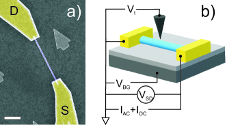
The diameter of the wire was nm. The wire was placed on an -type doped Si (100) substrate covered by a thermal grown 100 nm thick SiO2 insulating layer. The Si substrate served as the back-gate electrode. The Ti/Au contacts to the wire as well as the markers of the search pattern were defined by electron-beam lithography. The distance between the contacts was m. A scanning electron beam micrograph of the sample is shown in Fig. 1a). The source and drain metallic electrodes connected to the wire are marked as S and D.
All measurements were performed at K. The charged tungsten tip of a home-built scanning probe microscope [17] was used as a mobile gate during scanning gate imaging measurements, see Fig. 1b). All scanning gate measurements were performed by keeping the potential of the scanning probe microscope tip (=0 V) as well as the back-gate voltage () constant. The conductance of the wire during the scan was measured in a two-terminal circuit by using a standard lock-in technique. The tip to SiO2 surface distance chosen for the scanning process was nm. During SGM scans and linear magnetotransport measurements a driving AC current with an amplitude of nA at a frequency of 231 Hz was applied while the voltage was measured by a differential amplifier. External magnetic field was directed perpendicular to the wire axis and Si substrate surface.
3 Experimental results
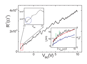
In Fig. 2 the dependence of conductance () of the nanowire as a function of back gate voltage is presented. The overall linear dependence of conductance on back gate voltage (carrier density) is typical for Si-doped InAs nanowires [15]. Non-regular fluctuations are universal conductance fluctuations (UCF) which arise because the phase coherence length in InAs is comparable to the length of the wire. The magnified low back gate section of curve is shown in the top-left inset of Fig. 2. Additionally to the UCF, there are oscillations with period of mV, marked with blue oval. These oscillations come from the residual Coulomb blockade of a quantum dot positioned in the mid of the nanowire [18].
According to finite element calculations of the capacitance of the nanowire [19], the specific capacitance of our sample is pF/m. Thus, it is possible to calculate the carrier density of the nanowire as a function of the back gate voltage , here V is the threshold voltage, and the elastic mean free path . The low-right inset in Fig. 2 shows the dependencies of (black curve, left scale) and (blue curve, right scale) on back-gate voltage, here is the Fermi vector. Two green arrows point to the curve at V and 1 V. It is worth noting that the variations of and as changes from -1 V to 1 V is just 25-30%.
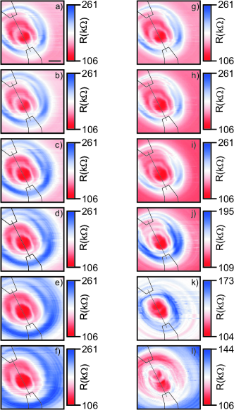
The results of SGM mapping of the nanowire are presented in Figs. 3 – 8. Each figure demonstrates the evolution of the scanning results due to weak variation of the back gate voltage with a step of 10 mV (Figures a) to f)), and applied external magnetic field ( T, 0.2 T, 0.3 T, 0.5 T, 1 T, and 2 T, Figures g) to l)) for six back gate voltages, i.e. V, V, V, 1 V, 4 V, and 10 V, respectively. The step of of 10 mV was chosen to exceed correlation back gate voltage mV for all applied , here is the diffusion coefficient.
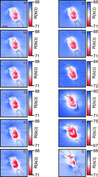
Mapping results of the SGM scanning in the vicinity of V presented in Fig. 3 demonstrate quite complex structure typical for nanowires or nanotubes with a number of the blocking barriers of different opacity [20]. The key feature of scans in Fig. 3 is well defined concentric ovals, see Figs. 3f) and 3l) for example. The presence and the position of such ovals means the formation of the quantum dot in the mid-section of the nanowire and ovals are the result of the Coulomb blockade realized in this dot [20]. The period of Coulomb blockade oscillations of mV obtained from curve allows to estimate the length of electronic system of this quantum dot nm. Taking into account the lengths of depletion zones of around 100 nm, the distance between two strong blocking barriers forming this dot can be estimated as nm. Thus, this quantum dot is positioned approximately in the center of the wire with barrier-to-barrier distance . It means that the InAs nanowire is divided into three sections. The Section I extends from the source contact to the first blocking barrier, the Section II is the quantum dot itself and the Section III lays between the second blocking barrier and the drain contact.
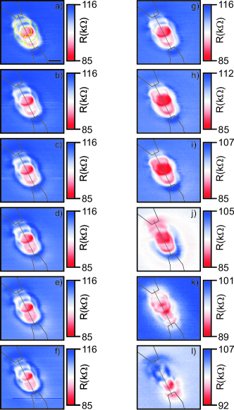
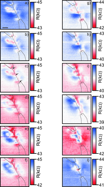
The scanning gate microscopy mapping performed in the vicinity of V is shown in Fig. 4. At this back gate voltage the SGM mapping results look still quite complex, see Fig. 4a), but they demonstrate a response from all three sections of the nanowire. Here equicapacitance ovals and circles are not resulted from the Coulomb blockade, because the shape of them changes dramatically with application of external magnetic field, see Figs. 4g) – 4l). The equicapacitance ovals and circles in SGM data come from the alteration of the opacity of the blocking barriers or, probably, due to the variation of the density of states [2].
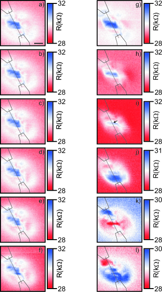
Fig. 5 shows the scanning gate microscopy mapping carried out in the vicinity of V. No well-defined response from each of the Sections can be resolved, but the mapping results are extremely stable against the back gate voltage variation and application of magnetic field up to T, see Figs. 5a) – 5h). Higher magnetic fields from T to 2 T deform the SGM mapping results, similar to Fig. 4, see Figs. 5j) – 5l).
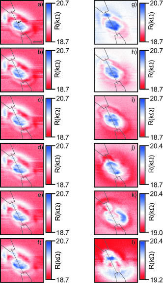
The scanning gate microscopy mapping done in the vicinity of V is presented in Fig. 6. Both the variation of back gate voltage and the magnetic field as small as 0.1 T alter the SGM mapping pictures. The smallest scale features of SGM scans have the size of 250 – 300 nm. This size is comparable to the tip to SiO2 surface distance and it is the spatial resolution of the current experimental setup [21]. Three well-defined resistance minima are visible in scans and marked with arrows in Fig. 6c). As it has been estimated previously, the distance between two barriers forming the central quantum dot is 250 nm and each of the barrier cannot be resolved separately, so they are visualized as a single one. Thus, these three minima are related to the source contact barrier, quantum dot double barrier, and the drain contact barrier. The positions of them are stable against variation of (Figs. 6a) – 6f)). The double barrier sign (the red spot marked with arrow) is visible even at SGM scan done at T, see Fig. 6l). The scans shown in Fig. 6 additionally confirm the position of the quantum dot allocated from SGM mapping, see Fig. 4.
The SGM mapping done in the vicinity of V and 10 V is shown in Fig. 7 and 8, respectively. These scans demonstrate the interplay of the features come from UCF which vary their positions and the residual impact of the blocking barriers on the wire conductivity. It is worth noting that some minor influence of these barriers in SGM scans remains both at V (Fig. 7i)) and at V (Fig. 8a)). This behavior of blocking barrier influence on SGM mapping is the same as observed in InN nanowires previously [3].
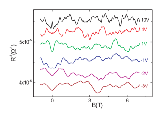
Figure 9 shows the dependence of the wire conductance () on magnetic field ( T T) measured at V, V, V, 1 V, 4 V, and 10 V, i.e almost at the same values of the back gate voltages as for SGM scans. Curves, except one measured at 10 V, are shifted for clarity. Non-regular reproducible oscillations are UCF. The peak in conductivity around T for 10 V comes from weak antilocalization quantum correction due to spin-orbit interaction in InAs and it transforms to the localization dip for V. This transition from weak anilocalization to localization with decreasing the carrier concentration is typical for InAs nanowires [22, 23, 24, 25, 26, 27].
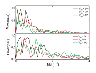
The top panel of Fig. 10 shows universal conductance fluctuations spectra calculated from data measured at V, V, and V. The bottom panel of Fig. 10 presents the spectra measured at 1 V, 4 V, and 10 V. The essential suppression of the fluctuation spectra for (T-1) for top panel data in comparison to bottom panel data is clearly visible.
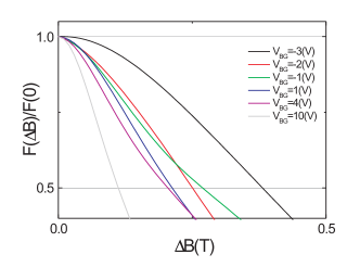
The normalized correlator dependencies calculated from magnetoconductance data obtained at V, V, V, 1 V, 4 V, and 10 V are integrated in Fig. 11. The smallest value of the correlation field T extracted from data measured at 10 V gives nm. This value of the phase correlation length is within the range from 200 nm to 500 nm of previously obtained values [22, 23, 24, 25, 26, 27]. The significant increase of value at higher carrier density has been obtained previously as well [22, 23, 24]. The correlator is calculated from data measured in magnetic fields from T to 7 T to eliminate any influence of low-field quantum corrections.
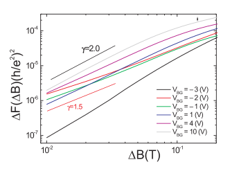
The dependencies of deviation of the correlator in double logarithmic scale for V, V, V, 1 V, 4 V, and 10 V are shown in Fig. 12. Two straight lines show the slopes of dependence for two exponent values (red) and (black).
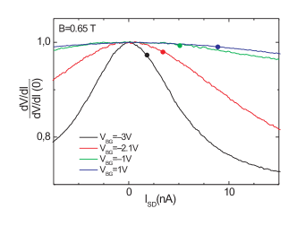
The normalized differential resistance as a function of driving current measured at V, V, V, and 1 V are shown in Fig. 13. The dots on the curves mark values of current where . The well-defined non-linear behavior is seen for V and V only. This experiment is done at T to eliminate the quantum corrections influence.
4 Discussion
Transitions from Coulomb blockade to Fabri-Pérot interference in ballistic one-dimensional and quasi-one-dimensional systems were recently observed and discussed in detail in [30, 31]. In inhomogeneous diffusive quasi-one-dimensional systems, the transport phenomena are more complex. Presented data help to illustrate all relevant transport regimes focusing on their peculiarities in magnetotransport data and the SGM mapping results obtained in the same run.
The doped InAs nanowire is chosen because of its homogeneous radial carrier density [15]. Thus, any influence on the transport resulted from cylindrical shape of the electronic system [32] is minor.
As it has been mentioned previously, the dependence (Fig. 2) and SGM data (Fig. 3) obtained at V allow to estimate the position and the size of the quantum dot formed in the mid-section of the wire. The spectrum of the UCF (see Fig. 10, top panel) confirms the statement that the dominating role belongs to the small area loops ( nm2). The transport at this value of the back gate voltage is non-linear, see Fig. 13.
By increasing the carrier density concentration ( V), we transfer the system to non-linear resonant regime (see Fig. 13). In this regime, the strongest resonant scatters (blocking barriers) define three quasi-localized states formed in corresponding Sections of wire. Maps obtained with the SGM technique depend weakly on variation of the back gate voltage and application of the small magnetic field, see Fig. 3. New energy scale of the order of 100 meV is the characteristic energy of variation of opacity of the blocking barriers and fluctuation of the density of states. The contribution from small area loops is dominant in the UCF spectra (Fig. 10, top panel).
Further increase of the carrier concentration ( V) gives rise to the reduced influence of the blocking barriers. Transport becomes linear, see Fig. 13. No well-defined patterns allocating three Sections of the nanowire can be observed in SGM scans, but the resonant reflections of electrons still play an important role altering the local carrier density of states and ruling the weak dependence of the SGM mapping results on the back gate voltage and the magnetic field (Fig. 4), similarly to previously described non-linear resonant regime. Contribution from small area loops is still dominant in the UCF spectrum (Fig. 10, top panel). The size of the area of these loops allows to estimate the maximum characteristic length of segments into which the nanowire is divided nm .
At V we observe important changes in the SGM scans. The SGM mapping results (Fig. 5) become sensitive to the small (10 mV) increase of the back gate voltage as well as to application of the small ( T) external magnetic field. This situation is similar to the one obtained previously in undoped InAs nanowires [33] and can be considered as diffusive regime with diminished influence of resonant scatters. Additionally, the spectrum of the UCF extends to the higher frequencies, thus the larger area loops start to come into play (Fig. 10, bottom panel). Transport is linear as indiated in Fig. 13.
Further increasing the back gate voltage results in even more homogeneous transport according to SGM data (Figs. 6 and 7) with wide spectra of UCF (Fig. 10, bottom panel). At V correlation field has reached the value related to the phase coherence length of 200 nm, finally.
The transiton from linear resonant regime to more homogenous diffusive one occurs at back gate voltages between V and 1 V (see two arrows in the bottom-right inset of Fig. 2). As it has been mentioned previously, no essential variations of or happen in this range of back gate voltages. Therefore, it is not possible to find any sign of this transition just from dependence. But the correlated switch of the behavior of SGM mapping results, as well as sudden increase of the high frequency spectrum of UCF can be considered as an undoubtful evidence of this transition.
The most exciting feature of the obtained data is non-trivial behavior of the exponent in dependencies obtained for different back gate voltages, see Fig. 13. This exponent is for Coulomb blockade regime when the transport is defined mostly by quantum dot. Then, the value of exponent drops to values close to in non-linear and linear resonant scattering regimes, see Table 1. The transport depends strongly on resonant scatters in the wire forming a set of quasilocalized states resulting in nonhomogeneous fractional Bownian motion of magnetoconductance dependence with dimensionality greater than one () [8, 12] for both non-linear and linear resonant regimes. The reason of weak variation of in this regime is presently not clear and might be the subject for further investigations. At V when the role of the resonance scatters diminishes, the value of starts to rise toward to the standard value of 2, see Table. 1.
| (T) | ||
|---|---|---|
| -3 | 0.48 | 2.1 |
| -2 | 0.25 | 1.38 |
| -1 | 0.27 | 1.42 |
| 1 | 0.21 | 1.78 |
| 4 | 0.21 | 1.71 |
| 10 | 0.11 | 1.90 |
According to the underlying paper by Altshuler, Gefen, Kamenev and Levitov (AGKL), there are three regimes of many-body localization [34, 35]. The first one is realized when the energy is less than the characteristic energy of interacting quantum dot ( V meV, and it is the Coulomb blockade regime in this paper). In this regime, one-particle states are very similar to the exact many-body states. Here is the normalized conductance of the central quantum dot. In the intermediate regime when meV at V, the quasiparticle states are delocalized, but they are fractal and non-ergodic [34, 35]. Here is the Thouless energy of the typical largest segment of the wire formed by resonant scatters.
Fractal structure of wave function of the electronic system and overall non-ergodic behavior of this regime correlates well with in the current experiment at non-linear and linear resonant regimes demonstrating fractional Bownian motion of magnetoconductance behavior. It is worth noting that the value of Fermi length is nm at V, this means that the number of channels in the nanowire is , and the localization length is nm. This value is comparable to and to the actual phase-coherence length for V, i.e. VVV nm nm. Thus, the many body localization is possible in each segment ( V). Finally, when is the largest energy scale (eV), a simple exponential decay of the quasiparticle life time is set again, here is the Thouless energy of the whole wire. This regime corresponds to the homogenous diffusive transport regime in the current work.
Thus, as in AGKL theoretical picture so in the current experiment there is a special regime with non-trivial behavior of the electronic system wave function or fractal Bownian motion of magnetoconductance curve lying in between Coulomb blockade and homogenous diffusion transport regimes.
There are quite a number of theoretical papers in which quasi-localized states formed by resonant scatters are considered as a possible origin of formation of the observed fractional Bownian motion of magnetoconductance dependence in the intermediate regime [36, 37, 38]. However, there have been no clear experimental evidences or visualizations of such kind of states. Here we show as the SGM mapping scans visualize them and hence the fractional Bownian motion they initiate.
5 Conclusion
We performed the low temperature measurements of the magnetotransport in doped InAs nanowire in the presence of a charged tip of an atomic force microscope serving as a mobile gate. By varying the carrier concentration, the system under investigation passes through four transport regimes from Coulomb blockade to homogeneous diffusive transport. Fractional Bownian motion of magnetoconductance dependence is observed in non-linear and linear resonant transport regimes. Two key experiments for demonstration of transition from the linear resonant transport regime to the diffusive one are presented. The experimental results are in general agreement with the theoretical model proposed by AGKL.
6 Acknowledgements
The authors would like to thank Chrisian Blömers for samples preparation and Raffaella Calarco for nanowire growth. This work is supported by the RSF grant 23-22-00141, https://rscf.ru/project/23-22-00141/.
References
References
- [1] Datta S (1995) ”Electronic transport in mesoscopic systems”, Cambridge University Press.
- [2] Altshuler B L and Aronov A G in Electron–Electron Interactions in Disordered Conductors, Ed. by A. J. Efros and M. Pollack (Elsevier Science, North-Holland, 1985).
- [3] Zhukov A A 2022 JETP.
- [4] Imry Y, ”Introduction to Mesoscopic Physics”, Oxford University Press, Oxford (1997).
- [5] Altshuler B L (1985) Pisma Zh. Eksp. Teor. Fiz. 41 530-533; (1985) JETP Lett. 41, 648-651.
- [6] Lee P A, Stone A D and Fukuyama H 1987 Phys. Rev. B 35 1039-70.
- [7] Beenakker C W J and van Houten H 1988 Phys. Rev. B 37 6544.
- [8] Ketzmerick R 1996 Phys. Rev. B 54 10841.
- [9] Mandelbrot B B, The Fractal Geometry of Nature (Freeman, San Francisco, 1982).
- [10] Jannsen M 1994 International Journal of Modern Physics B 08 943-984.
- [11] Evers F and Mirlin A D 2008 Rev. Mod. Phys. 80 1355.
- [12] Hegger H, Huckestein B, Hecker K, Janssen M, Freimuth A, Reckziegel G and Tuzinski R 1996 Phys. Rev. Lett. 77 3885.
- [13] Marlow C A, Taylor R P, Martin T P, Scannell B C, Linke H, Fairbanks M S, Hall G D R, Shorubalko I, Samuelson L, Fromhold T M, Brown C V, Hackens B, Faniel S, Gustin C, Bayot V, Wallart X, Bollaert S and Cappy A 2006 Phys Rev B 73 195318
- [14] Amin K R, Ray S S, Pal N et al. 2018 Commun Phys 1 1. https://doi.org/10.1038/s42005-017-0001-4
- [15] Wirths S, Weis K, Winden A, Sladek K, Volk Ch, Alagha S, Weirich T E, von der Ahe M, Hardtdegen H, Lüth H, Demarina N, Grützmacher D and Schäpers Th 2011 J. Appl. Phys. 110 053709
- [16] Akabori M, Sladek K, Hardtdegen H, Schäpers Th and Grützmacher D 2009 J. Cryst. Growth 311 3813.
- [17] Zhukov A A 2008 Instrum. Exp. Tech. 51 130-4
- [18] Weis K, Wirths St, Winden A, Sladek K, Hardtdegen H, Lüth H, Grützmacher D and Schäpers Th 2014 Nanotechnology 25 135203.
- [19] Wunnicke O 2006 Appl. Phys. Lett. 89 083102.
- [20] Woodside M T and McEuen P L 2002 Science 296 1098.
- [21] Zhukov A A, Volk Ch, Winden A, Hardtdegen H and Schäpers Th 2014 J. Phys. Condens. Matter 26 165304.
- [22] Bleszynski A C, Zwanenburg F A, Westervelt R M, Roest A L, Bakkers E P A M and Kouwenhoven L P 2005 Nano Lett. 7 2559-62
- [23] Dhara S, Solanki H S, Singh V, Narayanan A, Chaudhari P, Gokhale M, Bhattacharya A and Deshmukh M M 2009 Phys. Rev. B 79 121311(R)
- [24] Roulleau P, Choi T, Riedi S, Heinzel T, Shorubalko I, Ihn T and Ensslin K 2010 Phys. Rev. B 81 155449
- [25] Blömers C, Lepsa M I, Luysberg M, Grützmacher D, Lüth H, and Schäpers Th 2011 Nano Lett. 11 3550-6
- [26] Boyd E E, Storm K, Samuelson L and Westervelt R M 2011 Nanotechnology 22 185201
- [27] Wang L B, Guo J K, Kang N, Pan D, Li S, Fan D, Zhao J and Xu H Q 2015 Appl. Phys. Lett. 106 173105.
- [28] Takase K, Ashikawa Y, Zhang G, Tateno K and Sasaki S 2017 Scientific Reports 7 930
- [29] Liang D, Du J and Gao X P A 2010 Phys. Rev. B 81 153304.
- [30] Makarovski A, Liu J, Finkelstein G 2007 Phys. Rev. Lett. 99 066801.
- [31] Wang L B, Pan D, Huang G Y, Zhao J, Kang N and Xu H Q 2019 Nanotechnology 30 124001.
- [32] Lüth H, Blömers Ch, Richter Th, Wensorra J, Estévez Hernández S, Petersen G, Lepsa M, Schäpers Th, Marso M, Indlekofer M, Calarco R, Demarina N and Grützmacher D 2010 Phys. Status Solidi C 7 386-9
- [33] Zhukov A A, Volk Ch, Winden A, Hardtdegen H and Schäpers Th 2014 J. Phys. Condens. Matter 26 165304.
- [34] Altshuler B L, Gefen Y, Kamenev A and Levitov L S 1997 Phys. Rev. Lett. 78 2803.
- [35] Mirlin A D and Fyodorov Y V 1997 Phys. Rev. B 56 13393.
- [36] Altshuler B L, Kravtsov V E, and Lerner I V 1987 JETP Lett. 45 199.
- [37] Muzykantskii B A and Khmelnitskii D E 1995 Phys. Rev. B 51 5480.
- [38] Mirlin A D 1995 JETP Lett. 62 603.