Probing and control of guided exciton-polaritons in a 2D semiconductor-integrated slab waveguide
Abstract
Guided 2D exciton-polaritons, resulting from the strong coupling of excitons in semiconductors with non-radiating waveguide modes, provide an attractive approach towards developing novel on-chip optical devices. These quasiparticles are characterized by long propagation distances and efficient nonlinear interaction but cannot be directly accessed from the free space. Here we demonstrate a powerful approach for probing and manipulating guided polaritons in a Ta2O5 slab integrated with a WS2 monolayer using evanescent coupling through a high-index solid immersion lens. Tuning the nanoscale lens-sample gap allows for extracting all the intrinsic parameters of the system. We also demonstrate the transition from weak to strong coupling accompanied by the onset of the motional narrowing effect: with the increase of exciton-photon coupling strength, the inhomogeneous contribution to polariton linewidth, inherited from the exciton resonance, becomes fully lifted. Our results enable the development of integrated optics employing room-temperature exciton-polaritons in 2D semiconductor-based structures.
keywords:
Guided polaritons, excitons, strong coupling, transition metal dichalcogenides, solid immersion lens, motional narrowing.School of Physics and Engineering, ITMO University, St. Petersburg, 197101, Russia \abbreviationsTMD, SIL, BFP
![[Uncaptioned image]](/html/2305.12858/assets/TOCSILNOTFORSUBMISSIONONLYFORDEMONSRATION.jpg)
Polaritonics has attracted substantial attention as a promising base for devices utilizing non-linear effects. Polaritons arise from strong coupling between light and resonant transition in matter and manifest themselves in the energy spectrum as Rabi splitting 1. One of the promising materials for polaritonics is transition metal dichalcogenides (TMDs) 2. In their monolayer limit, TMDs are direct bandgap semiconductors 3, and their optical response is dominated by the excitonic resonance4. TMD excitons possess high oscillator strength with large binding energy, and they are stable in ambient conditions 5, which makes these materials ideal candidates for room-temperature polaritonic devices 6.
The strong light–matter coupling regime with exciton-polariton formation can be achieved by coupling excitonic resonances in TMD monolayers to confined optical modes supported by distributed Bragg reflector (DBR) mirrors7, 8, 9, 10, plasmonic structures 11, 12, 13, or subwavelength gratings14, 15. However, the polariton propagation length in such structures is limited by their radiative decay rates and small group velocity. In contrast, guided polaritons 16, 17, where excitons couple to non-radiating waveguide modes with large group velocity, are characterized by long-range propagation up to hundreds of 18, which is very useful for the integration in photonic circuits. This, combined with sizeable polariton–polariton interaction, leads to a number of technologically important non-linear optical effects such as soliton formation 19, 20, lasing 21, and self-phase modulation 19. In addition, unpatterned waveguide structures supporting guided polaritons require far fewer and significantly cheaper fabrication processes.
Exciton-polaritons in planar unpatterned structures have been studied in different material platforms 22, 18 including bulk TMD crystals 23, 24. Due to the non-radiating nature of guided polaritons, probing their dispersion in experiment is challenging. One approach is provided by scattering-type scanning near-field optical microscopy 25, 26, 27. While it offers nanoscale lateral spatial resolution and provides access to the information on phase and propagation lenghts of the waveguide modes, it requires complex and time-consuming measurements based on raster-scanning the sample with a near-field probe and does not allow to controllably tune the parameters of the system under study.
Another approach relies on the use of high-NA oil-immersion objectives 28, 23, 29. It allows imaging of the polariton dispersion in a single optical measurement but does not provide means for controlling the parameters of the strongly coupled system and is limited to room conditions due to the use of immersion oil.
In this work, we probe and control guided exciton-polaritons in monolayer WS2 integrated with a 90-nm-thick Ta2O5 waveguide using the approach based on attenuated total internal reflection 30. To excite and detect the polaritons, which are intrinsically uncoupled from free-space waves and propagate below the light line, we use Fourier-plane microscopy with a solid immersion lens (SIL) 31. The use of SIL with an accurately controlled distance to the sample surface allows us not only to probe the polariton dispersion but also to tune the radiative losses of the waveguide mode, thus controlling the regime of strong coupling. Notably, this technique does not require the use of edges/defects to create standing polariton waves and therefore provides a powerful microscopy tool for a wide range of samples, which is compatible with various advanced optical spectroscopic methods, e.g., nonlinear optical spectroscopy based on harmonics generation, parametric down conversion, or four-wave mixing processes. Our results establish a novel approach to study and control guided exciton-polaritons in 2D semiconductors and provide a basis for future investigations of radiative/non-radiative losses, lifetimes, and nonlinearities in systems supporting guided polaritons.
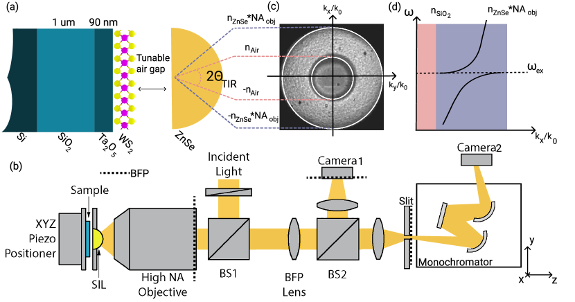
The system under study is shown in Figure 1(a). WS2 monolayer was mechanically exfoliated from bulk crystal and dry transferred on 90-nm-thick Ta2O5 optical single-mode waveguide on Si/SiO2 substrate, with the thickness of SiO2 spacer of 1 . We note that the waveguide thickness is chosen such that only the fundamental guided TE mode is supported in the spectral range of interest (see Supplementary Materials Figure S12). We used WS2 since it exhibits the most favorable ratio of the oscillator strength to exciton linewidth for achieving strong exciton–photon coupling at room temperature. The experimental scheme is shown in Figure 1(b). For excitation and detection of guided polaritons with large wavevectors, we combine evanescent wave coupling through SIL with a custom-built back focal plane (BFP) spectroscopy setup.
In the BFP spectroscopy part, the light coming from the beam splitter (BS1) is focused onto the sample by a microscope objective with a large numerical aperture (Mitutoyo, M Plan Apo HR, 100×, NA = 0.9). The reflected light passes through the 4f scheme, and the BFP of the objective is imaged onto a spectrometer slit coupled to a liquid-nitrogen-cooled imaging CCD Camera 2 (Princeton Instruments SP2500 + PyLoN), allowing us to observe reflection as a function of both wavevector and frequency. The slit cuts the BFP image in the direction at . Beamsplitter BS2 directs a part of the reflected light to Camera 1 (CMOSIS CMV300 USB3), which allows us to simultaneously observe the BFP image from the sample as shown in Figure 1(c) and capture dispersions with Camera 2 as schematically shown in Figure 1(d). We use an analyzer in the detection path to probe only TE waveguide modes for all reported measurements.
The in-plane wavevectors that can be accessed in an optical microscopy setup with a dry objective lens are limited by the numerical aperture, which does not exceed unity: . To overcome this limitation, we introduce a hemispherical SIL made of ZnSe in the optical path and use attenuated total internal reflection (TIR) to excite guided modes (characterized by larger wavevectors) in our sample evanescently. Figure 1(c) shows the BFP reflectance map obtained from a bare ZnSe lens. The light reflected from the center of the flat side of the lens can be separated into two regions: (i) with angles smaller than TIR angle shown in Figure 1(c) as the inner circle and (ii) with angles larger than TIR angle (outer circle). The inner region corresponds to , where is the air refractive index, as bulk waves exist in the air and manifest themselves as a dip in the center of Figure 1(c). In the outer circle , the waves propagating below the light line can exist in the air as evanescent waves. The resulting effective numerical aperture in our experiment is
| (1) |
where is the free space wavevector of light, and are speed and frequency of light, and nSIL stands for the refractive index of SIL. In our case , . Note that one can use a different material for SIL such as GaP, with refractive index , to achieve an even higher effective NA 3. The substrate of our sample has a 1 SiO2 spacer layer, so the states above the SiO2 light line leak to the substrate. We outline it with red color in Figure 1(d). The states with , where , are completely decoupled from the free space radiation in both substrate and air.
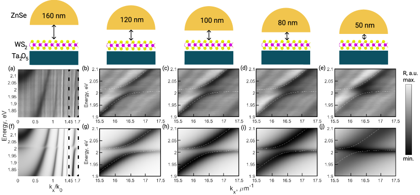
In the experiment, the sample is attached to a 3-axis piezo positioner. Moving along the and axes allows positioning the focal spot on a TMD monolayer, while moving in the z direction controls the SIL–sample gap. Figure 2(a-e) shows measured angle-resolved reflectance maps for different SIL–sample gaps as sketched in the top row. The interference fringes observed at in Figure 2(a),(f) correspond to the Fabry-Perot modes arising due to the presence of the SiO2 layer. Since the spectral positions of these fringes show a near-linear and sensitive dependence on the SIL–sample distance, we employ the comparison between measured and simulated normal-incidence reflectance spectra for calibrating the air gap values in the experimental data to best fit the dependencies in Figure 3 (a,b). The details on air gap calibration are given in Supplementary Materials Section 3.
In the measured angle-resolved reflectance maps shown in Figure 2(a-e), one can see the waveguide mode in the Ta2O5 layer at as highlighted with a dashed rectangle (see also Supplementary Materials Figure S1). The panels in Figure 2(b)-(e) show zoomed-in dispersion regions at the splitting between the guided mode and WS2 monolayer exciton resonance at the energy of 2.01 eV.
To support our experimental data, we perform numerical simulations using the T-matrix method 32. For Ta2O5 waveguide layer, we use refractive index data from Ref. 33 with increased losses fitted to account for additional scattering induced by the monolayer and SIL inhomogeneities. For excitons in WS2 monolayer, we use = 8.9 meV, meV, and E meV, where and are the radiative and non-radiative decay rates of exciton resonance with a total linewidth of , and Eexc represents the energy of the exciton resonance. Note that the non-radiative part accounts for various effects such as phonon scattering at room temperature, phonon-induced dephasing, and non-radiative recombination. The choice of these specific values is justified further in the text. The results of the simulations for different air gaps are shown in Figure 2(f-j).
Both experimental and simulated angle-resolved reflectance maps in Figure 2 show that, with the decrease of the SIL–sample gap, the waveguide mode becomes broader and the splitting between the exciton resonance and waveguide mode becomes less visible. To extract the SIL-induced modification of the reflectance and losses of the waveguide mode, we fit the dependence of reflectance on the in-plane wavevector at 2.05 eV for both experimental and simulated data with Fano line shapes (see Supplementary Materials Section 1 for the details on the fitting procedure). The large detuning from the exciton resonance (2.01 eV) ensures that the mode at this wavevector is close to being purely photonic. We then extract the SIL-induced reflectance modulation and mode linewidth as the amplitude and FWHM of the fitted Fano line shape, respectively.
The obtained reflectance modulation and total waveguide losses depending on SIL–sample distance are shown with back dots in Figure 3(a) and (b), respectively. Note that with the decrease of the SIL–sample gap, the waveguide mode radiative losses increase, while non-radiative ones originating from light absorption and scattering on defects remain the same. From the reflectance spectrum obtained for a specific gap, we can only extract the total linewidth (losses) of the mode , which is shown in Figure 3(b). The gap-independent nonradiative decay rate of the mode can be estimated using two different approaches. First, it can be obtained as the asymptotic value of total losses at large SIL–sample gaps when the radiative losses become negligible (horizontal dashed line in Figure 3(b)). Second, it can be estimated from the characteristic minimum of reflectance modulation at a specific gap seen in Figure 3(a), which corresponds to the critical coupling regime 31 where the radiative and nonradiative losses become equal to each other: (vertical dashed line). The nonradiative decay rate is then taken as half of the total linewidth at the point of critical coupling extracted from Figure 3(b).
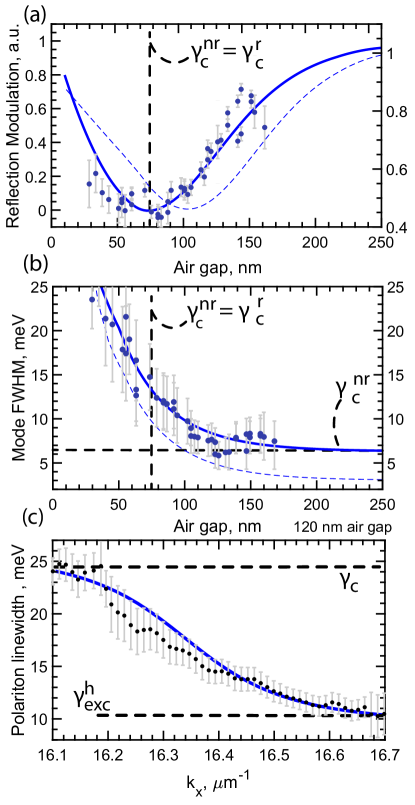
Comparison between the data extracted from the experiment and numerical results suggests the presence of additional losses, which we attribute to scattering at the TMD monolayer. To account for this scattering, we increase the imaginary part of the waveguide material (Ta2O5) refractive index in simulations. For comparison, the simulations with the original material dispersion are shown as dashed curves in Figure 3(a, b).
In contrast to the case of the photonic mode, the exciton resonance properties are not affected by the SIL for the experimental range of gaps, since the exciton size is at least an order of magnitude smaller than the air gaps studied in our experiment. Therefore, with the gaps above 10 nm, we tune only the radiative part of the waveguide mode losses, while excitonic properties remain intact. The difference in the effect of the SIL on the exciton and the waveguide mode resonances allows us to independently determine excitonic and waveguide losses from the experimental data, as discussed below.
Measured and simulated maps depending on the SIL–sample gap are shown in the Supplementary Materials video. A detailed description of the procedure we follow to fit the polariton dispersion is given in Supplementary Materials Section 2. As justified further, the waveguide mode is strongly coupled to the exciton resonance. This is manifested as Rabi splitting in the reflectance maps. One could expect the modification of the Rabi splitting with the alternation of waveguide mode losses in accordance with the relation:
| (2) |
where is the exciton-photon coupling strength. Dependencies of exciton-photon coupling strength and Rabi splitting on the SIL–sample gap extracted from the experimental data are shown in Figure 4(a) and (b). These plots can be split into two regions: (1) air gaps smaller than 50 nm, and (2) air gaps exceeding 50 nm. For larger gaps (Region 2), the field of the waveguide mode is weakly modified by SIL, and therefore the coupling strength only slightly depends on the air gap. In contrast, in Region 1, with the decrease of the SIL–sample gap, the mode field profile becomes strongly affected by the SIL, which is manifested by the drastic increase of its radiative losses.
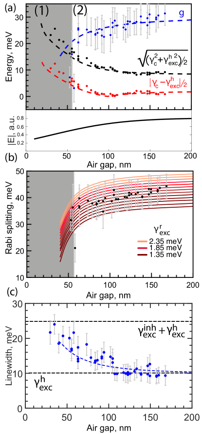
To confirm that the studied system is in the strong coupling regime, we check its parameters against the two strong coupling criteria. According to the first criterion, the value of the Rabi splitting should be real, which yields . In Figure 4(a), the left- and right-hand sides of this inequality, extracted from experimental data, are plotted with blue and red dots, respectively. One can see that the first criterion holds for all studied SIL–sample gaps. According to the second criterion, to spectrally resolve the upper and lower polaritonic resonances, the polariton splitting has to be greater than the sum of the linewidths of the upper and lower polariton branches, which is equivalent to . The right-hand side of this inequality is shown with black color in Figure 4(a). One can see that for SIL–sample gaps below nm this condition is no longer met. This transition is also clearly seen in Figure 2, where the splitting between the upper and lower polariton branches becomes indistinguishable in panels (e) and (j).
The two regions in Figure 4(a) and (b) therefore formally represent the strong (Region 2) and weak (Region 1, shaded area) coupling regimes. Note that in addition to the change in losses and thus in the imaginary part of the wavevector, its real part also changes for small air gaps, as shown in Supplementary Materials Figure S4. This is a fingerprint of the alternation of the mode effective refractive index stemming from the change in the mode field distribution in the presence of the high refractive index SIL separated from the sample by a small distance (below nm, Region 1). The two-oscillator model based on the unperturbed states we use for fitting the data becomes not applicable in this regime since the mode is not well-localized in the waveguide layer anymore.
The observed evolution of exciton-photon coupling with the increase of the air gap allows us to distinguish between the radiative and non-radiative decay rates of the exciton in the WS2 monolayer. The coupling strength between the exciton and waveguide resonances is related to the exciton oscillator strength as , where is the overlap integral defined by the mode profile 34. The exciton oscillator strength is, in turn, proportional to its radiative decay rate . Therefore, we can determine using the asymptotic value of the Rabi splitting for large air gaps, see Figure 4(b). Simulation results for different exciton radiative decay rates are shown in Figure 4(b) with solid lines. Comparing simulated and experimental data and minimizing the root mean square error (see Supplementary Materials Figure S5), we obtain the exciton radiative losses of meV. Since the homogeneous exciton linewidth is meV, we extract the exciton non-radiative decay rate as meV.
Remarkably, the homogeneous exciton linewidth extracted from the polariton dispersion is significantly smaller than the linewidth of the uncoupled exciton 35, which in our case is obtained from PL spectra as meV (see Supplementary Materials Figure S11). This difference stems from the fact that the inhomogeneous broadening in the strong coupling regime can be lifted due to the effect of motional narrowing36. Since changing the SIL–sample air gap allows us to achieve the transition from weak to strong coupling, we can study the onset of motional narrowing in our system. To do so, we plot the polariton linewidth at m-1 (corresponding to a high exciton fraction) as a function of the air gap, as shown in Figure 4(c).
For large air gaps, where the exciton–photon coupling strength is high and the motional narrowing effect is most pronounced, the polariton linewidth corresponds to the homogeneous linewidth of the exciton resonance . With the decrease of the gap, the coupling strength is gradually reduced, and the effect of motional narrowing eventually vanishes, such that the corresponding linewidth starts to include the inhomogeneous contribution: . In order to describe the observed experimenal result theoretically, we use a model recently proposed in literature37, as outlined in Supplementary Materials Section 2. The theoretical result is shown in Figure 4(c) with a dashed blue curve and demonstrates good agreement with the experimental data. The observed pronounced dependence of the polariton linewidth on the SIL–sample gap in the transition between strong and weak light–matter coupling is an important manifestation of the polariton motional narrowing effect. Thus, by tuning the geometrical parameters of our experimental scheme, we demonstrate control on the motional narrowing effect, with the ability to switch on and off the inhomogeneous broadening of excitons in monolayer semiconductors.
1 Conclusion
In summary, in this work, we directly probe guided exciton-polaritons in a planar TMD-based waveguide. To access their dispersion below the light line, we use a solid immersion lens combined with the back focal plane spectroscopy technique. Careful measurement of angle-resolved reflectance maps as a function of SIL–sample air gap enables reversible control of the waveguide and exciton-polariton dispersions. Our experimental results combined with numerical simulations allow us to retrieve the parameters of the system, which include: radiative and nonradiative decay rates of the exciton resonance, as well as the dependence of corresponding rates for the optical mode on the SIL–sample distance. Additionally, we demonstrate control on exciton-polariton coupling strength via SIL-induced rearrangement of the local electromagnetic field in the polaritonic waveguide. Utilizing the transition from weak to strong coupling regime, we experimentally observe the onset of the motional narrowing effect and demonstrate control on the inhomogeneous broadening of polaritons. The suggested approach is suitable for probing guided polaritons in arbitrary planar structures and can be employed in various fields including active and nonlinear topological polaritonics.
Sample fabrication was supported by Priority 2030 Federal Academic Leadership Program. Optical measurements were funded by Russian Science Foundation, project 21-72-10100. Theoretical modelling was funded by Russian Science Foundation, project 21-12-00218. A.K.S. acknowledges TU Dortmund core funds.
Extraction of polariton properties from the reflectance measurements, fit of the polariton dispersion, calibration of air gap in the experiment, estimation of polariton propagation lengths, extraction of exciton radiative lifetime, angle-resolved photoluminescence measurements, field distribution of the fundamental waveguide mode in the presence of SIL.
Supplementary video: evolution of angle-resolved reflectance maps with the change of the SIL–sample air gap.
References
- Khitrova et al. 2006 Khitrova, G.; Gibbs, H. M.; Kira, M.; Koch, S. W.; Scherer, A. Vacuum Rabi splitting in semiconductors. Nature Physics 2006, 2, 81–90
- Schneider et al. 2018 Schneider, C.; Glazov, M. M.; Korn, T.; Höfling, S.; Urbaszek, B. Two-dimensional semiconductors in the regime of strong light-matter coupling. Nature Communications 2018, 9, 2695
- Mak and Shan 2016 Mak, K. F.; Shan, J. Photonics and optoelectronics of 2D semiconductor transition metal dichalcogenides. Nature Photonics 2016, 10, 216–226
- Wang et al. 2018 Wang, G.; Chernikov, A.; Glazov, M. M.; Heinz, T. F.; Marie, X.; Amand, T.; Urbaszek, B. Colloquium: Excitons in atomically thin transition metal dichalcogenides. Rev. Mod. Phys. 2018, 90, 021001
- Chernikov et al. 2014 Chernikov, A.; Berkelbach, T. C.; Hill, H. M.; Rigosi, A.; Li, Y.; Aslan, B.; Reichman, D. R.; Hybertsen, M. S.; Heinz, T. F. Exciton Binding Energy and Nonhydrogenic Rydberg Series in Monolayer . Phys. Rev. Lett. 2014, 113, 076802
- Gu et al. 2019 Gu, J.; Chakraborty, B.; Khatoniar, M.; Menon, V. M. A room-temperature polariton light-emitting diode based on monolayer WS2. Nature Nanotechnology 2019, 14, 1024–1028
- Dufferwiel et al. 2015 Dufferwiel, S. et al. Exciton–polaritons in van der Waals heterostructures embedded in tunable microcavities. Nature Communications 2015, 6, 8579
- Dufferwiel et al. 2018 Dufferwiel, S.; Lyons, T. P.; Solnyshkov, D. D.; Trichet, A. A. P.; Catanzaro, A.; Withers, F.; Malpuech, G.; Smith, J. M.; Novoselov, K. S.; Skolnick, M. S.; Krizhanovskii, D. N.; Tartakovskii, A. I. Valley coherent exciton-polaritons in a monolayer semiconductor. Nature Communications 2018, 9, 4797
- Wurdack et al. 2021 Wurdack, M.; Estrecho, E.; Todd, S.; Yun, T.; Pieczarka, M.; Earl, S.; Davis, J.; Schneider, C.; Truscott, A.; Ostrovskaya, E. Motional narrowing, ballistic transport, and trapping of room-temperature exciton polaritons in an atomically-thin semiconductor. Nature Communications 2021, 12, 1–8
- Zhao et al. 2021 Zhao, J.; Su, R.; Fieramosca, A.; Zhao, W.; Du, W.; Liu, X.; Diederichs, C.; Sanvitto, D.; Liew, T. C.; Xiong, Q. Ultralow threshold polariton condensate in a monolayer semiconductor microcavity at room temperature. Nano Letters 2021, 21, 3331–3339
- Sun et al. 2021 Sun, J.; Li, Y.; Hu, H.; Chen, W.; Zheng, D.; Zhang, S.; Xu, H. Strong plasmon–exciton coupling in transition metal dichalcogenides and plasmonic nanostructures. Nanoscale 2021, 13, 4408–4419
- Jiang et al. 2019 Jiang, P.; Song, G.; Wang, Y.; Li, C.; Wang, L.; Yu, L. Tunable strong exciton–plasmon–exciton coupling in WS 2–J-aggregates–plasmonic nanocavity. Optics Express 2019, 27, 16613–16623
- Liu et al. 2016 Liu, W.; Lee, B.; Naylor, C. H.; Ee, H.-S.; Park, J.; Johnson, A. C.; Agarwal, R. Strong exciton–plasmon coupling in MoS2 coupled with plasmonic lattice. Nano Letters 2016, 16, 1262–1269
- Kravtsov et al. 2020 Kravtsov, V. et al. Nonlinear polaritons in a monolayer semiconductor coupled to optical bound states in the continuum. Light: Science & Applications 2020, 9, 56
- Zhang et al. 2018 Zhang, L.; Gogna, R.; Burg, W.; Tutuc, E.; Deng, H. Photonic-crystal exciton-polaritons in monolayer semiconductors. Nature Communications 2018, 9, 713
- Beggs et al. 2005 Beggs, D.; Kaliteevski, M.; Brand, S.; Abram, R.; Kavokin, A. Waveguide polaritons: interaction of a quantum well exciton with an electromagnetic mode of a planar waveguide. Physica Status Solidi (c) 2005, 2, 787–790
- Walker et al. 2013 Walker, P.; Tinkler, L.; Durska, M.; Whittaker, D.; Luxmoore, I.; Royall, B.; Krizhanovskii, D.; Skolnick, M.; Farrer, I.; Ritchie, D. Exciton polaritons in semiconductor waveguides. Applied Physics Letters 2013, 102, 012109
- Liran et al. 2018 Liran, D.; Rosenberg, I.; West, K.; Pfeiffer, L.; Rapaport, R. Fully guided electrically controlled exciton polaritons. ACS Photonics 2018, 5, 4249–4252
- Walker et al. 2019 Walker, P. M.; Whittaker, C. E.; Skryabin, D. V.; Cancellieri, E.; Royall, B.; Sich, M.; Farrer, I.; Ritchie, D. A.; Skolnick, M. S.; Krizhanovskii, D. N. Spatiotemporal continuum generation in polariton waveguides. Light: Science & Applications 2019, 8, 1–11
- Walker et al. 2015 Walker, P.; Tinkler, L.; Skryabin, D.; Yulin, A.; Royall, B.; Farrer, I.; Ritchie, D.; Skolnick, M.; Krizhanovskii, D. Ultra-low-power hybrid light–matter solitons. Nature Communications 2015, 6, 1–7
- Suárez-Forero et al. 2020 Suárez-Forero, D.; Riminucci, F.; Ardizzone, V.; De Giorgi, M.; Dominici, L.; Todisco, F.; Lerario, G.; Pfeiffer, L.; Gigli, G.; Ballarini, D.; others Electrically controlled waveguide polariton laser. Optica 2020, 7, 1579–1586
- Pirotta et al. 2014 Pirotta, S.; Patrini, M.; Liscidini, M.; Galli, M.; Dacarro, G.; Canazza, G.; Guizzetti, G.; Comoretto, D.; Bajoni, D. Strong coupling between excitons in organic semiconductors and Bloch surface waves. Applied Physics Letters 2014, 104, 051111
- Munkhbat et al. 2018 Munkhbat, B.; Baranov, D. G.; Stuhrenberg, M.; Wersall, M.; Bisht, A.; Shegai, T. Self-hybridized exciton-polaritons in multilayers of transition metal dichalcogenides for efficient light absorption. ACS Photonics 2018, 6, 139–147
- Gogna et al. 2020 Gogna, R.; Zhang, L.; Deng, H. Self-hybridized, polarized polaritons in ReS2 crystals. ACS Photonics 2020, 7, 3328–3332
- Hu et al. 2019 Hu, F.; Luan, Y.; Speltz, J.; Zhong, D.; Liu, C.; Yan, J.; Mandrus, D.; Xu, X.; Fei, Z. Imaging propagative exciton polaritons in atomically thin WSe 2 waveguides. Physical Review B 2019, 100, 121301
- Iyer et al. 2022 Iyer, R. B.; Luan, Y.; Shinar, R.; Shinar, J.; Fei, Z. Nano-optical imaging of exciton–plasmon polaritons in WSe 2/Au heterostructures. Nanoscale 2022, 14, 15663–15668
- Luan et al. 2022 Luan, Y.; Zobeiri, H.; Wang, X.; Sutter, E.; Sutter, P.; Fei, Z. Imaging anisotropic waveguide exciton polaritons in tin sulfide. Nano Letters 2022, 22, 1497–1503
- Shin et al. 2022 Shin, D.-J.; Cho, H.; Sung, J.; Gong, S.-H. Direct Observation of Self-Hybridized Exciton-Polaritons and Their Valley Polarizations in a Bare WS2 Layer. Advanced Materials 2022, 2207735
- Canales et al. 2023 Canales, A.; Kotov, O.; Shegai, T. O. Perfect Absorption and Strong Coupling in Supported MoS2 Multilayers. ACS Nano 2023, 17, 3401–3411
- Otto 1968 Otto, A. Excitation of nonradiative surface plasma waves in silver by the method of frustrated total reflection. Zeitschrift für Physik A Hadrons and nuclei 1968, 216, 398–410
- Permyakov et al. 2021 Permyakov, D. V.; Kondratiev, V.; Pidgayko, D.; Sinev, I. S.; Samusev, A. K. Probing optical losses and dispersion of fully guided waves through critical evanescent coupling. JETP Letters 2021, 113, 780–786
- Waterman 1965 Waterman, P. Matrix formulation of electromagnetic scattering. Proceedings of the IEEE 1965, 53, 805–812
- Rodríguez-de Marcos et al. 2016 Rodríguez-de Marcos, L. V.; Larruquert, J. I.; Méndez, J. A.; Aznárez, J. A. Self-consistent optical constants of SiO2 and Ta2O5 films. Optical Materials Express 2016, 6, 3622–3637
- Koshelev et al. 2018 Koshelev, K.; Sychev, S.; Sadrieva, Z. F.; Bogdanov, A. A.; Iorsh, I. Strong coupling between excitons in transition metal dichalcogenides and optical bound states in the continuum. Physical Review B 2018, 98, 161113
- Selig et al. 2016 Selig, M.; Berghäuser, G.; Raja, A.; Nagler, P.; Schüller, C.; Heinz, T. F.; Korn, T.; Chernikov, A.; Malic, E.; Knorr, A. Excitonic linewidth and coherence lifetime in monolayer transition metal dichalcogenides. Nature communications 2016, 7, 13279
- Whittaker et al. 1996 Whittaker, D.; Kinsler, P.; Fisher, T.; Skolnick, M.; Armitage, A.; Afshar, A.; Sturge, M.; Roberts, J. Motional narrowing in semiconductor microcavities. Physical Review Letters 1996, 77, 4792
- Osipov et al. 2023 Osipov, A. N.; Iorsh, I. V.; Yulin, A. V.; Shelykh, I. A. Transport regimes for exciton-polaritons in disordered microcavities. 2023; \urlhttps://arxiv.org/abs/2305.16112, [Online; accessed August 18, 2023]