Proposal of a free-space-to-chip pipeline for transporting single atoms
Abstract
A free-space-to-chip pipeline is proposed to efficiently transport single atoms from a magneto-optical trap to an on-chip evanescent field trap. Due to the reflection of the dipole laser on the chip surface, the conventional conveyor belt approach can only transport atoms close to the chip surface but with a distance of about one wavelength, which prevents efficient interaction between the atom and the on-chip waveguide devices. Here, based on a two-layer photonic chip architecture, a diffraction beam of the integrated grating with an incident angle of the Brewster angle is utilized to realize free-space-to-chip atom pipeline. Numerical simulation verified that the reflection of the dipole laser is suppressed and that the atoms can be brought to the chip surface with a distance of only . Therefore, the pipeline allows a smooth transport of atoms from free space to the evanescent field trap of waveguides and promises a reliable atom source for a hybrid photonic-atom chip.
I Introduction
In recent decades, neutral atoms have become one of the most important systems for realizing quantum information processing, and their potential applications have attracted increasing attention Monroe (2002); Wehner et al. (2018); Chang et al. (2018). Quantum systems based on single atoms can demonstrate nonclassical effects and verify quantum theory Beugnon et al. (2006), and have been extended to quantum computing and quantum communication Saffman et al. (2010); Schäfer et al. (2020); Weiss and Saffman (2017); Briegel et al. (2000); Specht et al. (2011). Among these schemes, optical dipole traps have become a common tool for trapping and manipulating neutral cold atoms, which have a low atomic scattering rate, especially for far detuned frequencies Schlosser et al. (2001); Kaufman and Ni (2021). Various configurations of optical dipole traps have been proposed and investigated in recent decades Kim et al. (2019); Nayak et al. (2019); Liu et al. (2022a); Frese et al. (2000); Ton et al. (2022). Additionally, optical cavities have been introduced to enhance the interaction between atoms and photons Raimond et al. (2001); Reiserer and Rempe (2015), and the strong coupling between arrays of atoms Liu et al. (2022b); Chen et al. (2022a); Deist et al. (2022) and multiple cavities Daiss et al. (2021); Reiserer (2022) are demonstrated recently. With these advantages, optical dipole traps and optical cavities have become a main platform for realizing atom-based quantum optics devices.
With the rapid development and maturity of integrated optical technology, quantum information devices call for integrating atoms into photonic chips Chang et al. (2018, 2019); Béguin et al. (2020); Luan et al. (2020); Liu et al. (2022c); Wang et al. (2022). Compared with conventional atom and cavity systems, such a hybrid photonic-atom chip system has many advantages, including the high stability and robustness of the system, strongly enhanced light-matter interaction with tightly confined optical modes, flexibility to engineer the long-range interaction, and great extensibility of devices on a single chip. In addition, it also has the potential to realize atom cooling by photonic chips Chen et al. (2022b); Dyer et al. (2022); Isichenko et al. (2022). Therefore, the hybrid photonic-atom chip allows the cooling, transport, stable on-chip trapping, manipulation of single atoms, and promises a compact solution for quantum optics devices.
However, it is very challenging to bring cold atoms from the free space magneto-optics trap to the surface of the chip with a subwavelength distance Kim et al. (2019); Zhou et al. (2023); Bouscal et al. (2023). This is because the evanescent field on a photonic chip decays significantly in vacuum, thus a stable on-chip atom trapping demands an atom-surface distance of around , nonetheless the scattering of the dipole laser on the chip surface prevents the atoms from approaching the chip. While several methods have been proposed to transport cold atoms from free space to photonic chips Kuhr et al. (2001); Thompson et al. (2013); Burgers et al. (2019); Will et al. (2021), achieving efficient and precise atom delivery beyond the limit of the "last one micron" remains a critical area of exploration for the advancement of atomic chips. One potential approach to circumvent the problem is introducing anti-reflection coating and the Brewster angle Jannasch et al. (2012); Cheng et al. (2016); Hoenig and Moebius (1991) to the photonics chip, which can prevent the scattering of light on the surface.
In this work, a hybrid photonic-atom chip platform is proposed for realizing an efficient free-space-to-chip pipeline, which allows efficient transport of single atoms to an on-chip evanescent field trap. A free space optical conveyor belt could be realized by the interference of the diffracted beam from the integrated apodized grating (AG) and the Gaussian beam, which intersects with a waveguide-based on-chip optical conveyor belt. By utilizing the anti-reflection of the Brewster angle, the reflection of the free space dipole trap on the waveguide surface is efficiently suppressed, which makes the atom delivery continuously from the free space to the integrated waveguide surface with a distance of around . The pipeline provides a potential solution for reliable and efficient single-atom sources on the chip, which is essential for future atom-based quantum optics devices.
The paper is organized as follows. Section II provides an overview of the operation procedure for the hybrid photonic-atom chip architecture. Section III covers the structure design of the atom pipeline and the impact of reflection. In Sec. IV, the reflection on the dielectric surface is analyzed, and it can be suppressed by the Brewster angle. Finally, Sec. V demonstrates the performance of the atom pipeline with the anti-reflection based on the Brewster angle.
II Overview
Figure 1 sketches the two-layer chip architecture for realizing free-space-to-chip atom transportation. On the top layer, the photonic structures are fabricated to be vacuum-cladded, thus cold atoms can be transported and trapped on top of them. As demonstrated in previous works, the blue- and red-detuned lasers in the waveguide could create a dipole trap by evanescent fields with a trap depth of mK Barnett et al. (2000); Hammes et al. (2003); Le Kien et al. (2004); Stievater et al. (2016). The integrated waveguides and microring resonators not only allow the trap potential for manipulating the matter-wave of single atoms, but also enhance the photon-atom interaction due to the strongly confined optical fields on the chip, thus this platform provides a unique platform for realizing hybrid photonic-atomic quantum circuits Chang et al. (2019); Luan et al. (2020); Béguin et al. (2020); Liu et al. (2022c); Wang et al. (2022). The bottom layer of the chip provides the key optical components for converting the guided laser light in the waveguide into free space beams, preparing cold atoms and transporting the atoms to the top layer. The advantage of these on-chip components is a unified platform of free space optical components, allowing very compact realization of the whole system, which is very robust against perturbations and reduces the difficulties in aligning lasers.
The working procedure of this architecture is as follows:
(i) Preparation of a cold atom cloud with a distance of around above the chip, as shown in Fig. 1(a)-(1). In most cold atom experiments, the cold atom ensemble can be efficiently prepared by a standard magneto-optics trap (MOT) Metcalf and van der Straten (1999). We can choose a photonic chip with transparent substrates Liu et al. (2022c), and thus a conventional six-beam MOT configuration could be realized, with the MOT center very close to the chip Kim et al. (2019); Xu et al. (2023). It also has the potential to realize MOTs with on-chip optical devices. For instance, bottom-layer photonic circuits could provide three cooling laser beams via gratings, and the MOT could be realized by introducing an additional off-chip free space cooling laser and a printed circuit for the magnetic field gradient Chen et al. (2022b); Dyer et al. (2022); Isichenko et al. (2022).
(ii) Use an optical conveyor belt to transport cold atoms to the surface of the chip. An apodized grating (AG) on the bottom-layer could generate a focused Gaussian laser beam. The waveguide mode (WGM) on the under layer is diffracted by the apodized grating with a diffraction angle in the substrate and then output with a refraction angle in the air at wavelength as shown in Fig. 1(a)-(2). A Gaussian beam (GB) with the same wavelength propagates in the opposite direction to interfere with the diffraction beam (DB) and forms an optical lattice above the surface of the chip, which enables the transport of atoms through the atomic conveyor belt technique Kuhr et al. (2003). By intersecting the free space standing-wave conveyor belt with the on-chip evanescent field-based conveyor belt Schneeweiss et al. (2013), atoms could be transported between the two dipole traps Miroshnychenko et al. (2006) and an atom pipeline could be realized.
(iii) Trapping and guiding single atoms by the top-layer waveguide structures as shown in Fig. 1(a)-(3). When the trapped atoms reach the chip surface (top layer) with a distance of about , the Casimir-Polder interaction increases rapidly McLachlan (1964), which will attach the atom to the chip surface and keep the atoms from moving to other positions on the chip. The blue-detuned TM (transverse magnetic) mode and the red-detuned TE (transverse electric) mode are incident on the waveguide. The evanescent field of the blue-detuned TM mode can provide a repulsive force to overcome the Casimir-Polder interaction and prevent the atom from being attached to the chip surface. The evanescent field of the red-detuned TE mode can provide an attractive force on the atom, and the combination of the evanescent field of the waveguide modes and the Casimir-Polder interaction forms the optical trap well, and its center is about above the waveguide surface.
Following the above procedure, it is a potential method to transport the atoms from the MOT to the integrated photonic structures. However, as mentioned above, due to the potential diffraction and reflection of optical lasers around the surface, it is very challenging to realize a smooth intersection between the optical conveyor belt and the on-chip evanescent field traps. In this work, we focus on such an intersection and provide a practical solution of the pipeline connecting the free space and the chip. We consider the 87Rb atoms, with a D2 transition wavelength of . For the optical conveyor belt, we select a red-detuned laser to form the standing-wave optical trap well. For the evanescent field trap, we select the blue-detuned TM mode with wavelength and the red-detuned TE mode with wavelength to propagate in the waveguide unidirectionally and bidirectionally, respectively.
III Structure design for the pipeline
The detailed design parameters for realizing the pipeline are illustrated in Fig. 1(b). For the chip architecture, we choose for the two layers of photonic structures, with thicknesses and . It is worth noting that the condition is ultilized as the anti-reflection condition for the laser in the top layer. Since the optical path length of light in the layer is related to the incident angle, the thickness of the top layer for anti-reflection is optimized by the numerical simulations. The bottom layer is buried in , with a distance from the top layers of . The apodized grating is etched on a tapered waveguide with a taper angle of and the apex of the taper up-surface is selected as the origin of the coordinate system, and the etching depth of the grating is set to be . The length of the grating part is about , and the width of the input waveguide is . More details about the design of the apodized grating can be found in Ref. Liu et al. (2022a). The diffraction angle of the apodized grating is related to the grating period . To form a Gaussian-like beam, the grating period of the apodized grating is gradually changed from to , and the duty cycle increases from 0.5 to 0.3 along the grating. On the top layer, a waveguide intersects with the output Gaussian-like beam for transporting the atoms from the optical conveyor belt to the waveguide evanescent field trap. Here, to suppress the diffraction of the free space beam, the top layer of is almost uniform, with only two grooves (width ) etched to form a waveguide (width ) in the center.
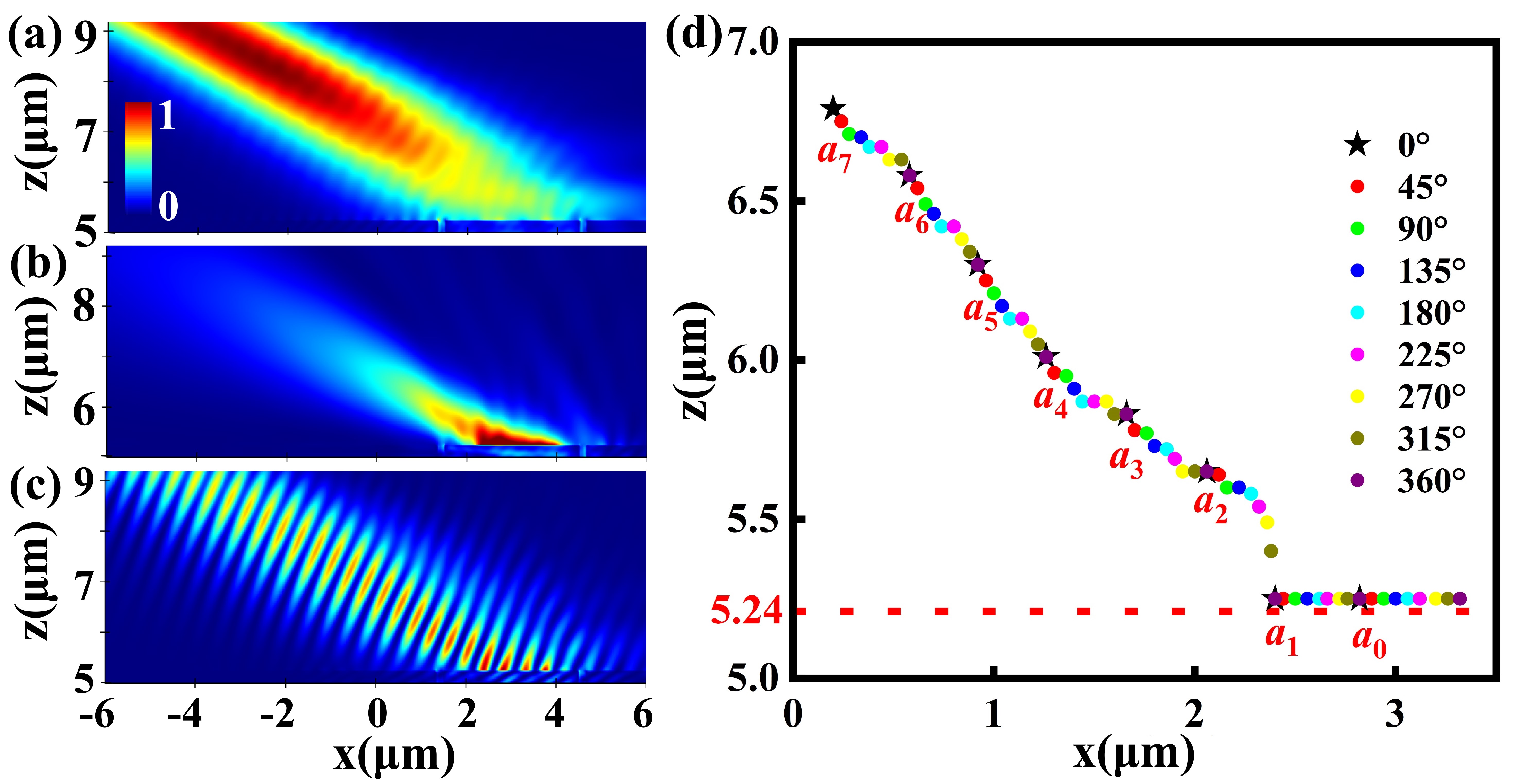
Through three-dimensional numerical simulation of the electromagnetic field distribution by the finite-different time-domain (FDTD) method, the performance of the pipeline is investigated in Fig. 2. To analyze the effect of the reflection on the chip surface, the top layer without the etched grooves is considered first. A Gaussian beam of TE mode with a waist diameter of is incident on the chip surface. At the same time, a counter-propagating beam from the apodized grating on the bottom-layer, which is the diffraction output from the TE mode, transmits through the top-layer with an angle of 51.525∘. To form the standing-wave fields for the optical conveyor belt, the Gaussian beam incident with the same angle of 51.525∘, which is different from the Brewster angle. The electric field distributions of the Gaussian beam and the diffraction beam on the plane above the chip is shown in Fig. 2(a) and (b), respectively. Although the anti-reflection condition is taken into our design, we can still find non-negligible reflection of optical fields, which induced the interference field distribution close to the surface of the chip. As shown by the insets of Figs. 2(a) and (b), the field distribution of the cross section shows a similar Gaussian-like beam profile. With input from both free space and the bottom-layer, the interference of the Gaussian beam gives rise to the standing-wave optical lattice, as shown in Fig. 2(c). The antinodes of the standing wave are denoted by , , ,…, , where the antinode with increasing index is far away from the chip surface.
For the wavelength of 850 nm, which is the red-detuned light for the 87Rb atom, the optical lattice can trap cold 87Rb atoms at the antinodes. Consequently, by controlling the phase difference between the two inputs for the Gaussian beam and the diffraction beam, it is anticipated that the atoms trapped in the antinodes could move toward the chip Kuhr et al. (2003); Miroshnychenko et al. (2006); Kim et al. (2019). In practical experiments, the two inputs are generated from the same laser, with phase control realized by an acousto-optics modulator and a radio-frequency (RF) signal generator Xu et al. (2023). In Fig. 2(d), the evolution of the antinode locations from to are plotted for various , and the positions of with are denoted by stars. If the antinode with reaches the position of the antinode with , the trapped atom can be transported from to by changing the phase difference of . For a desired atom pipeline, the antinode moves and connects with the antinode with a phase difference variation of , and atoms in the optical lattice can be continuously transported to . However, we found that the traces of the antinodes are not continuous, and are separated into three sections. This means that the atoms from the free space, such as initially at , could only be transported to about above the chip and could not be transported to or . The reason for this discontinuity is due to the reflection of the top-layer that forms an additional standing-wave pattern [Fig. 2(a)] and prevents atom transport toward the chip surface.
IV The suppression of reflection
The above results confirmed that a -distance limits the application of optical conveyor belts in the hybrid photonic-atom chip, and there is considerable reflection of laser power even when the top-layer thickness satisfies the antireflection condition. To circumvent this problem, we introduce the Brewster angle to further suppress the reflection, i.e. the Gaussian beam with the TM mode is incident on the chip surface with an input angle equal to the Brewster angle of the top-layer. As shown in Fig. 3(a), the reflection coefficients of optical fields on a flat surface for two polarizations follow Ra et al. (1973)
| (1) | |||||
| (2) |
where and are the refractive index of media 1 to media 2. For our case, light with wavelength incident from air () to (=1.999), the reflectivities and as functions of the incident angle are plotted in Fig. 2(b). We found that at the so-called Brewster angle , the reflection coefficients vanish, and the reflection is significantly suppressed.
According to Eq. 1, the reflection of the Gaussian beam with TM mode will vanish when incident on the chip surface with the Brewster angle . Compared with Fig. 2(a), the reflection of the Gaussian beam on the chip surface, as shown in Fig. 4(a), is suppressed both in the near field and the far field. The diffraction beam with the TM mode is output from the top layer with the same Brewster angle , when the TM mode is incident on the apodized grating with grating periods ranging from to . The intensity distribution of the diffraction beam on the plane is shown in Fig. 4(b), with the inset as the intensity distribution on the cross section denoted by the white dotted line. The counter-propagating Gaussian beam and the diffraction beam interfere to form an optical lattice as shown in Fig. 4(c). The relation between the antinode locations ( to ) and the phase difference are given in Fig. 4(d). In contrast to the discontinuous traces of antinodes, the scheme employing the Brewster angle generates a continuous trace of antinodes toward the interface, as all the antinodes with move and connect to with . As a result, the trapped atoms can be transported from the free space to very close to the chip surface. After the atoms are delivered to reach the chip surface, they can be trapped and transported further by the optical trap well on the waveguide surface, and the pipeline can be realized.
V The performances of the atom pipeline
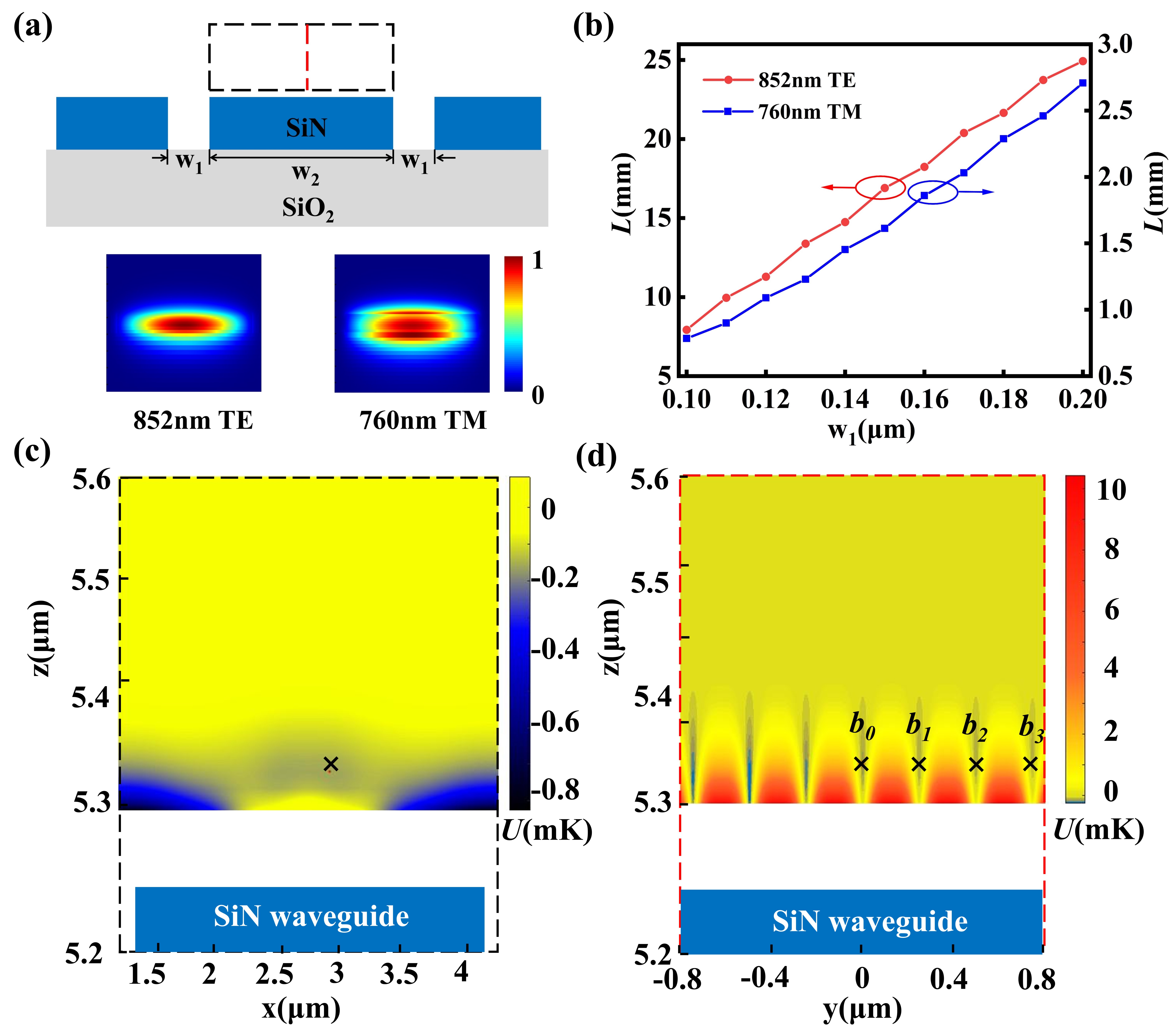
In practice, we should fabricate waveguides for the smooth pipeline connecting the free space MOT and the on-chip evanescent field atom trap. On the top layer of the chip, two grooves are etched to form a waveguide, which intersects with the optical lattice at the right angle. On the one hand, we should make a waveguide with a small cross-section to effectively enhance the electric field intensity of the waveguide mode, thus saving the required laser power for the evanescent field trap. On the other hand, the width of the two grooves should be as small as possible because the etched grooves may influence on the optical lattice by introducing the scattering of the dipole trap laser. Considering such a trade-off relation, we choose and . Figure 5(a) depicts the cross-section structure of the waveguide, plots the corresponding electric-field distribution for blue- and red-detuned trap lasers, and shows confined modes in the waveguide region. Due to the leakage loss to the unetached slab for a finite groove width, the mode intensity should decay with propagation as , with being the mode propagation length in the waveguide. Figure 5(b) numerically investigated the propagation length against , and both modes have a propagation length exceeding , which indicates an energy loss less than for a waveguide length less than when realizing the pipeline. In the area of the chip surface covered by the free space dipole laser beam, which has a diameter of several micrometers, minimizing the grooves around the waveguide are minimized for a small diffraction loss of the beam, while the width of the waveguide is increased and the length of this narrow groove regime is to suppress the leakage of waveguide modes into the unetched slab. Outside the laser spot area, a tapered waveguide can be used to narrow the waveguide, resulting in stronger coupling between the atom and the waveguide mode. Additionally, the width of the groove can be increased to avoid leakage loss. Here, the difference between the TE and TM modes is attributed to the different electric-field boundary conditions for orthogonal optical polarizations and thus different leakage losses through tunneling the gap .
In the following, the optical trap depth is analyzed. By ignoring the Zeeman sublevels, the optical dipole potential formed by the linear polarization light can be estimated as
| (3) |
where is the natural linewidth of the 87Rb D2 transition, is the saturation intensity the cyclic transition, is the intensity of the optical field, and are the detunings between the light frequency and the and transitions, which exceed the hyperfine splitting of the excited state. For the 87Rb atom with a resonant wavelength of about , the gradient force formed by a red-detuned optical field ( or ) is an attractive force, and that formed by a blue-detuned optical field () is a repulsive force. In the calculation of the optical dipole potential, the reference point is set at infinity with .
When the atom approaches the surface of chip with a small distance, the Casimir-Polder potential also comes into play, which can be estimated as with represents the distance from the surface McLachlan (1964). The combination of the two-color evanescent field of the waveguide modes and the Casimir-Polder interaction results in an optical trap well above the surface of the waveguide. Figures 5(c) and (d) show the optical trap depths on the plane and plane above the waveguide surface corresponding to the black dashed rectangle and the red line in Fig. 5(a), where the powers of the blue- and red-detuned modes are and , respectively. A lattice of the trap well denoted by , ,… along the waveguide is generated, as shown in Fig. 5(d), with a distance between the trap centers and the waveguide surface of about . By manipulating the phase difference of the bidirectionally input red-detuned TE modes, the trap wells will move along the waveguide, which will transport the trapped atom to other positions of the chip. As a tradeoff for the reduced perturbations of the waveguide structure to the free space beams, the relatively wide waveguide requires a higher laser power for near-field optical dipole trap. A high power up to 10 W has been experimentally demonstrated for a waveguide mode on the optical chips Zhang et al. (2023), which makes it realistic for the laser power required in our designed waveguide. Though the tightly confined optical modes in the waveguide could induces the out-of-phase longitudinal polarization component, which may have an impact on potential of the atoms trapped in the evanescent field of a waveguide Lodahl et al. (2017); Junge et al. (2013). This impact on the potential is not discussed, since this manuscript mainly focuses on the transporting of atoms from free space to the chip surface.
For the free space conveyor belt, the intensity distributions for the case with etched grooves are shown in Figs. 6(a)-(c). Compared with Fig. 4(a)-(c), the scattering from the grooves induces a minor perturbation on the optical lattice’s intensity distribution, leading to a significant drop of the antinode position close to a1. When the atom approaches the waveguide surface to within hundreds of nanometer, the optical trap formed by the waveguide modes is employed to prevent the atom from attaching to the chip surface and to maintain a separation of about for the atom-waveguide coupling. Therefore, the sharp drop caused by the etched grooves does not destroy the atom delivery from the free space to the near field of the waveguide surface.
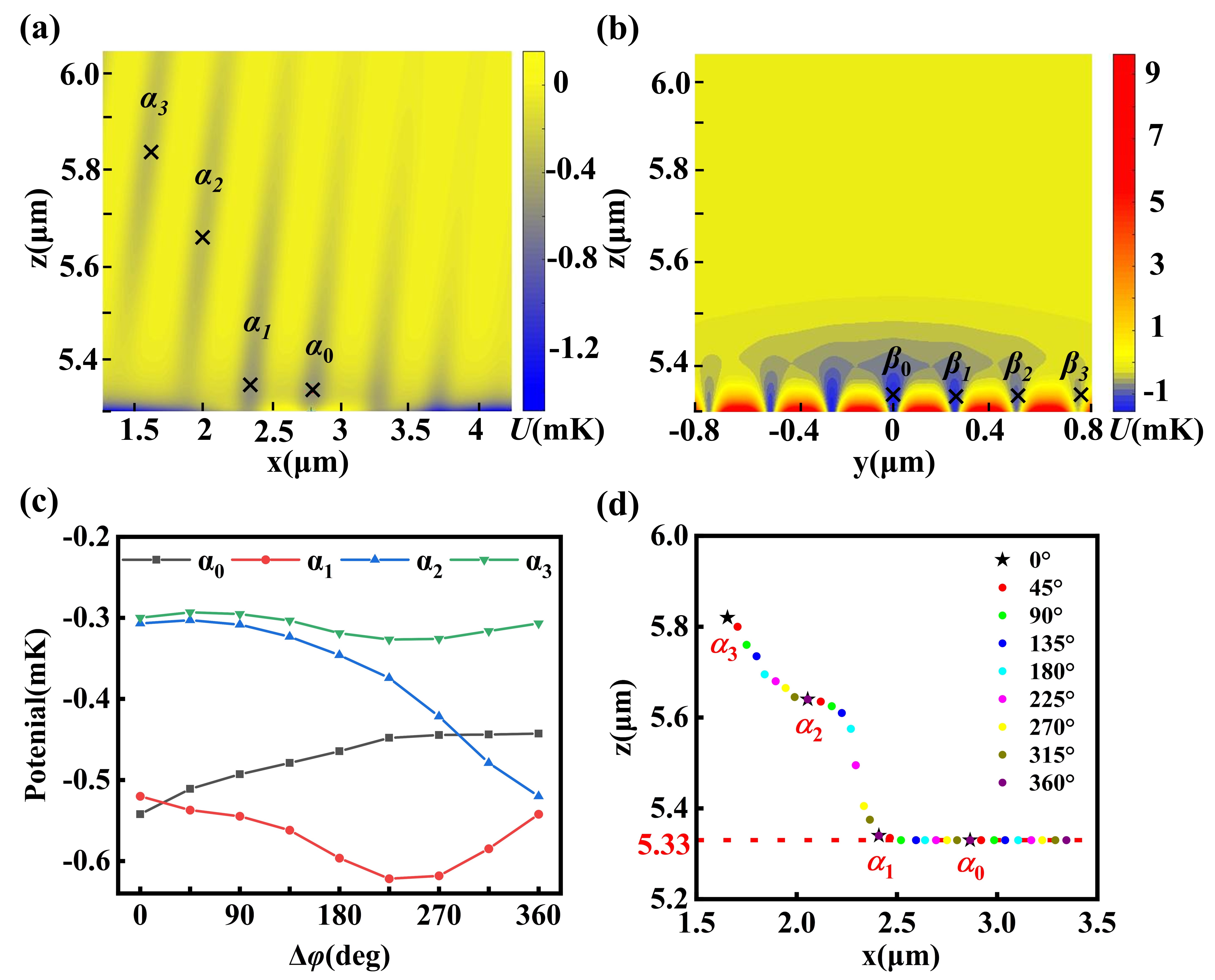
Last, when realizing the atom pipeline, the optical trap potential on the intersection is a superposition of potentials from the waveguide modes, the free space standing-wave, and the Casimir-Polder interaction. The distributions of the total optical trap potential of the intersection region with and for both free space and on-chip optical fields on the plane are shown in Fig. 7(a), and those on the plane are shown in Fig. 7(b). The powers of the Gaussian beam and the incident waveguide mode are and , respectively. The locations of trap wells are denoted by () along the free-space standing wave, and are denoted by () along the waveguide. By manipulating the phase difference of the free-space standing wave, the trap wells move and the effective trap depths vary. For example, Fig. 7(c) shows the results for to with the optical fields in the waveguide fixed (). To ensure a stable atom trap during atom delivery, trap depths deeper than are maintained. The trap centers of the wells vary with the phase difference , which shows a continue movement between the adjacent trap wells. Near the waveguide surface, trap well connects with trap well . The position of trap well will move horizontally to the adjacent trap well by manipulating the phase difference of the two red detuned TM modes, which will transport the atoms along the waveguide surface. Although the atom delivery of about several micrometer above the chip surface is considered above, it can also be achieved further away from the chip surface where a stable standing wave is achievable without the influence of reflection. Then, a continuous free-space-to-chip pipeline for single atoms is realized on the integrated chip.
VI Conclusion
A two-layer photonic chip architecture is proposed for realizing a compact hybrid photonic-atom chip. In particular, a key ingredient for realizing the efficient transportation of cold atoms from the free space magneto-optics trap to the integrated waveguide evanescent field trap is proposed and numerically validated. A free space optical conveyor belt is formed by the interference of an on-chip diffracted laser beam and a free space Gaussian light. However, due to the diffraction and reflection of the dipole laser, the atoms could only be transported close to the chip surface with a distance of about one wavelength. Thus, a free-space-to-chip pipeline for smooth delivery of single atoms is realized by introducing the Brewster angle to eliminate the reflection of dipole lasers on the surface of the chip. The continuous delivery of cold atoms from free space to the chip surface with a distance less than enables efficient interaction between the atoms and the evanescent field of the guided mode in the waveguides. Therefore, our proposal provides a reliable atom source for constructing on-chip hybrid atom-photonic devices, including single-photon sources, high-fidelity single-photon quantum gates, and quantum memories. Such a platform also promises a new type of integrated circuit for matter-waves of single atoms Amico et al. (2022).
VII Acknowledgments
We would like to thank Lei Xu and Ling-Xiao Wang for helpful discussions. This work was funded by the National Key R&D Program (Grant No. 2021YFA1402004 and No. 2018YFA0306400), the National Natural Science Foundation of China (Grants No. U21A6006, No. 12104441, No. 92265210, No. U21A20433, No. 62061160487 and No. 12074194), the Natural Science Foundation of Anhui Provincial (Grant No. 2108085MA17 and No. 2108085MA22), the Key Research and Development Program of Anhui Province (Grant No. 2022b1302007), and the Industrial Prospect and Key Core Technology Projects of Jiangsu Provincial Key R&D Program (Grant No. BE2022071). CLZ was also supported by the Fundamental Research Funds for the Central Universities and USTC Research Funds of the Double First-Class Initiative. The numerical calculations in this paper have been done on the supercomputing system in the Supercomputing Center of the University of Science and Technology of China. This work was partially carried out at the USTC Center for Micro and Nanoscale Research and Fabrication.
References
- Monroe (2002) C. Monroe, Nature 416, 238 (2002).
- Wehner et al. (2018) S. Wehner, D. Elkouss, and R. Hanson, Science 362, eaam9288 (2018).
- Chang et al. (2018) D. E. Chang, J. S. Douglas, A. González-Tudela, C.-L. Hung, and H. J. Kimble, Reviews of Modern Physics 90, 031002 (2018).
- Beugnon et al. (2006) J. Beugnon, M. P. a. Jones, J. Dingjan, B. Darquié, G. Messin, A. Browaeys, and P. Grangier, Nature 440, 779 (2006), arXiv:0610149 [quant-ph] .
- Saffman et al. (2010) M. Saffman, T. G. Walker, and K. Mølmer, Reviews of modern physics 82, 2313 (2010).
- Schäfer et al. (2020) F. Schäfer, T. Fukuhara, S. Sugawa, Y. Takasu, and Y. Takahashi, Nat. Rev. Phys. 2, 411 (2020).
- Weiss and Saffman (2017) D. S. Weiss and M. Saffman, Physics Today 70, 44 (2017).
- Briegel et al. (2000) H.-J. Briegel, T. Calarco, D. Jaksch, J. I. Cirac, and P. Zoller, Journal of modern optics 47, 415 (2000).
- Specht et al. (2011) H. P. Specht, C. Nölleke, A. Reiserer, M. Uphoff, E. Figueroa, S. Ritter, and G. Rempe, Nature 473, 190 (2011), arXiv:1103.1528 .
- Schlosser et al. (2001) N. Schlosser, G. Reymond, I. Protsenko, and P. Grangier, Nature 411, 1024 (2001).
- Kaufman and Ni (2021) A. M. Kaufman and K.-K. Ni, Nature Physics 17, 1324 (2021).
- Kim et al. (2019) M. E. Kim, T.-H. Chang, B. M. Fields, C.-A. Chen, and C.-L. Hung, Nature Communications 10, 1647 (2019).
- Nayak et al. (2019) K. P. Nayak, J. Wang, and J. Keloth, Phys. Rev. Lett. 123, 213602 (2019).
- Liu et al. (2022a) A. Liu, J. Liu, W. Peng, X.-B. Xu, G.-J. Chen, X. Ren, Q. Wang, and C.-L. Zou, Physical Review A 105, 053520 (2022a).
- Frese et al. (2000) D. Frese, B. Ueberholz, S. Kuhr, W. Alt, D. Schrader, V. Gomer, and D. Meschede, Phys. Rev. Lett. 85, 3777 (2000).
- Ton et al. (2022) K. Ton, G. Kestler, D. Filin, C. Cheung, P. Schneeweiss, T. Hoinkes, J. Volz, M. Safronova, A. Rauschenbeutel, and J. Barreiro, arXiv: 2211.04004 (2022).
- Raimond et al. (2001) J. M. Raimond, M. Brune, and S. Haroche, Reviews of Modern Physics 73, 565 (2001).
- Reiserer and Rempe (2015) A. Reiserer and G. Rempe, Reviews of Modern Physics 87, 1379 (2015).
- Liu et al. (2022b) Y. Liu, Z. Wang, P. Yang, Q. Wang, Q. Fan, G. Li, P. Zhang, and T. Zhang, arXiv: 2207.04371 (2022b).
- Chen et al. (2022a) Y.-T. Chen, M. Szurek, B. Hu, J. de Hond, B. Braverman, and V. Vuletic, Optics Express 30, 37426 (2022a).
- Deist et al. (2022) E. Deist, Y.-H. Lu, J. Ho, M. K. Pasha, J. Zeiher, Z. Yan, and D. M. Stamper-Kurn, Physical Review Letters 129, 203602 (2022).
- Daiss et al. (2021) S. Daiss, S. Langenfeld, S. Welte, E. Distante, P. Thomas, L. Hartung, O. Morin, and G. Rempe, Science 371, 614 (2021), arXiv:2103.13095 .
- Reiserer (2022) A. Reiserer, Reviews of Modern Physics 94, 041003 (2022), arXiv:2205.15380 .
- Chang et al. (2019) T.-H. Chang, B. M. Fields, M. E. Kim, and C.-L. Hung, Optica 6, 1203 (2019).
- Béguin et al. (2020) J.-B. Béguin, A. Burgers, X. Luan, Z. Qin, S.-P. Yu, and H. J. Kimble, Optica 7, 1 (2020).
- Luan et al. (2020) X. Luan, J.-B. Béguin, A. P. Burgers, Z. Qin, S.-P. Yu, and H. J. Kimble, Advanced Quantum Technologies 3, 2000008 (2020).
- Liu et al. (2022c) A. Liu, L. Xu, X.-B. Xu, G.-J. Chen, P. Zhang, G.-Y. Xiang, G.-C. Guo, Q. Wang, and C.-L. Zou, Physical Review A 106, 033104 (2022c).
- Wang et al. (2022) W. Wang, Y. Xu, and Z. Chai, Advanced Photonics Research 3, 2200153 (2022).
- Chen et al. (2022b) L. Chen, C.-J. Huang, X.-B. Xu, Y.-C. Zhang, D.-Q. Ma, Z.-T. Lu, Z.-B. Wang, G.-J. Chen, J.-Z. Zhang, H. X. Tang, C.-H. Dong, W. Liu, G.-Y. Xiang, G.-C. Guo, and C.-L. Zou, Phys. Rev. Appl. 17, 034031 (2022b).
- Dyer et al. (2022) S. Dyer, K. Gallacher, U. Hawley, A. Bregazzi, P. F. Griffin, A. S. Arnold, D. J. Paul, E. Riis, and J. P. McGilligan, arXiv: 2212.02853 (2022).
- Isichenko et al. (2022) A. Isichenko, N. Chauhan, D. Bose, J. Wang, P. D. Kunz, and D. J. Blumenthal, arXiv: 2212.11417 (2022).
- Zhou et al. (2023) X. Zhou, H. Tamura, T.-H. Chang, and C.-L. Hung, Physical Review Letters 130, 103601 (2023).
- Bouscal et al. (2023) A. Bouscal, M. Kemiche, S. Mahapatra, N. Fayard, J. Berroir, T. Ray, J.-J. Greffet, F. Raineri, A. Levenson, K. Bencheikh, C. Sauvan, A. Urvoy, and J. Laurat, arXiv: 2301.04675 (2023).
- Kuhr et al. (2001) S. Kuhr, W. Alt, D. Schrader, M. Muller, V. Gomer, and D. Meschede, Science 293, 278 (2001).
- Thompson et al. (2013) J. D. Thompson, T. Tiecke, N. P. de Leon, J. Feist, A. Akimov, M. Gullans, A. S. Zibrov, V. Vuletić, and M. D. Lukin, Science 340, 1202 (2013).
- Burgers et al. (2019) A. P. Burgers, L. S. Peng, J. A. Muniz, A. C. McClung, M. J. Martin, and H. J. Kimble, Proceedings of the National Academy of Sciences 116, 456 (2019).
- Will et al. (2021) E. Will, L. Masters, A. Rauschenbeutel, M. Scheucher, and J. Volz, Physical Review Letters 126, 233602 (2021), arXiv:2010.07267 .
- Jannasch et al. (2012) A. Jannasch, A. F. Demirörs, P. D. Van Oostrum, A. Van Blaaderen, and E. Schäffer, Nature Photonics 6, 469 (2012).
- Cheng et al. (2016) X. Cheng, Z. Song, J. Zhang, H. Jiao, B. Ma, Z. Sui, and Z. Wang, Optics Express 24, 24313 (2016).
- Hoenig and Moebius (1991) D. Hoenig and D. Moebius, The Journal of Physical Chemistry 95, 4590 (1991).
- Barnett et al. (2000) A. H. Barnett, S. P. Smith, M. Olshanii, K. S. Johnson, A. W. Adams, and M. Prentiss, Physical Review A 61, 023608 (2000).
- Hammes et al. (2003) M. Hammes, D. Rychtarik, B. Engeser, H.-C. Nägerl, and R. Grimm, Physical Review Letters 90, 173001 (2003).
- Le Kien et al. (2004) F. Le Kien, V. I. Balykin, and K. Hakuta, Physical Review A 70, 063403 (2004).
- Stievater et al. (2016) T. H. Stievater, D. A. Kozak, M. W. Pruessner, R. Mahon, D. Park, W. S. Rabinovich, and F. K. Fatemi, Optical Materials Express 6, 3826 (2016).
- Béguin et al. (2020) J.-B. Béguin, A. P. Burgers, X. Luan, Z. Qin, S. P. Yu, and H. J. Kimble, Optica 7, 1 (2020).
- Metcalf and van der Straten (1999) H. J. Metcalf and P. van der Straten, Laser Cooling and Trapping, Graduate Texts in Contemporary Physics (Springer New York, New York, NY, 1999).
- Xu et al. (2023) L. Xu, L.-X. Wang, G.-J. Chen, L. Chen, Y.-H. Yang, X.-B. Xu, A. Liu, C.-F. Li, G.-C. Guo, C.-L. Zou, and G.-Y. Xiang, Submitted (2023).
- Kuhr et al. (2003) S. Kuhr, W. Alt, D. Schrader, I. Dotsenko, Y. Miroshnychenko, W. Rosenfeld, M. Khudaverdyan, V. Gomer, A. Rauschenbeutel, and D. Meschede, Physical Review Letters 91, 213002 (2003), arXiv:0304081 [quant-ph] .
- Schneeweiss et al. (2013) P. Schneeweiss, S. T. Dawkins, R. Mitsch, D. Reitz, E. Vetsch, and A. Rauschenbeutel, Applied Physics B 110, 279 (2013), arXiv:1207.3021 .
- Miroshnychenko et al. (2006) Y. Miroshnychenko, W. Alt, I. Dotsenko, L. Förster, M. Khudaverdyan, D. Meschede, D. Schrader, and A. Rauschenbeutel, Nature 442, 151 (2006).
- McLachlan (1964) A. McLachlan, Molecular Physics 7, 381 (1964).
- Ra et al. (1973) J. W. Ra, H. Bertoni, and L. Felsen, SIAM Journal on Applied Mathematics 24, 396 (1973).
- Zhang et al. (2023) J. Zhang, Y. Kang, X. Guo, Y. Li, K. Liu, Y. Xie, H. Wu, D. Cai, J. Gong, Z. Shi, et al., Light: Science & Applications 12, 89 (2023).
- Lodahl et al. (2017) P. Lodahl, S. Mahmoodian, S. Stobbe, A. Rauschenbeutel, P. Schneeweiss, J. Volz, H. Pichler, and P. Zoller, Nature 541, 473 (2017).
- Junge et al. (2013) C. Junge, D. O’Shea, J. Volz, and A. Rauschenbeutel, Physical review letters 110, 213604 (2013).
- Amico et al. (2022) L. Amico, D. Anderson, M. Boshier, J.-P. Brantut, L.-C. Kwek, A. Minguzzi, and W. von Klitzing, Reviews of Modern Physics 94, 041001 (2022), arXiv:2107.08561 .