Electronic band structure change with structural transition of buckled Au2X monolayers induced by strain
Abstract
This study investigates the strain-induced structural transitions of and the changes in electronic band structures of Au2X (X=S, Se, Te, Si, Ge) and Au4SSe. We focus on Au2S monolayers, which can form multiple meta-stable monolayers theoretically, including -Au2S, a buckled penta-monolayer composed of a square Au lattice and S adatoms. The -Au2S is regarded as a distorted structure of -Au2S. Based on density functional theory (DFT) calculations using a generalized gradient approximation, the conduction and the valence bands of -Au2S intersect at the point, leading to linear dispersion, whereas -Au2S has a band gap of 1.02 eV. The conduction band minimum depends on the specific Au-Au bond distance, while the valence band maximum depends on both Au-S and Au-Au interactions. The band gap undergoes significant changes during the phase transition of Au2S induced by applying tensile or compressive in-plane biaxial strain to the lattice. Moreover, substituting S atoms with other elements alters the electronic band structures, resulting in a variety of physical properties without disrupting the fundamental Au lattice network. Therefore, the family of Au2X monolayers holds potential as materials for atomic scale network devices.
I Introduction
In recent years, many new structures of AB2-type 2D materials, such as transition metal dichalcogenides, have been proposed theoretically by high-throughput density functional theory (DFT) calculations [1, 2], and experimental material synthesis for database construction has also been actively carried out [3]. In our previous study, we performed high-throughput first-principles electronic structure calculations for AB2-type 2D materials based on DFT to construct a structure map which not only assembles families of 1T and 1H structures, such as the well-known transition metal dichalcogenides, but also highlights intriguing structural trends through the periodic table [4, 5].
In that study, we also found some characteristic monolayers (see Fig.10 in Ref. [4]), for example, Au2S [(90)], Au2B [(127)], and GeC2[(113)], which can be classified into a group of penta-monolayers. Here, the compound name and space group are described to represent a specific phase of monolayers. The difference among these three monolayers is how their structures are buckled. The Au2B [(127)] is a planar structure, while S atoms in the Au2S [(90)] are buckled as shown in Fig. 1 (b). The GeC2[(113)] is in the same space group of buckled pentagonal monolayers as PdSe2, which has already been synthesized experimentally [6]. The top view of Au2S [(90)] and Au2B [(127)] are similar pentagonal monolayers. A different perspective reveals that their structures consist of triangular and square Au lattice networks and S or B adatoms. For Au2S, there were some reports where Au2S has several phases [7, 8, 9]. In particular, a structure of Au2S [(129)], which consists of the square Au lattice networks and S adatoms as shown in Fig. 1 (a), is comprehended as a distorted structure of Au2S [(90)]. The geometrical structure of Au2S [(90)] and Au2S [(129)] have already been reported in the study about Cu2S [10, 11]. However, since Au2S [(90)] and Au2S [(129)] are not the most stable structure, researchers have not given a detailed analysis of the electronic structure of them.
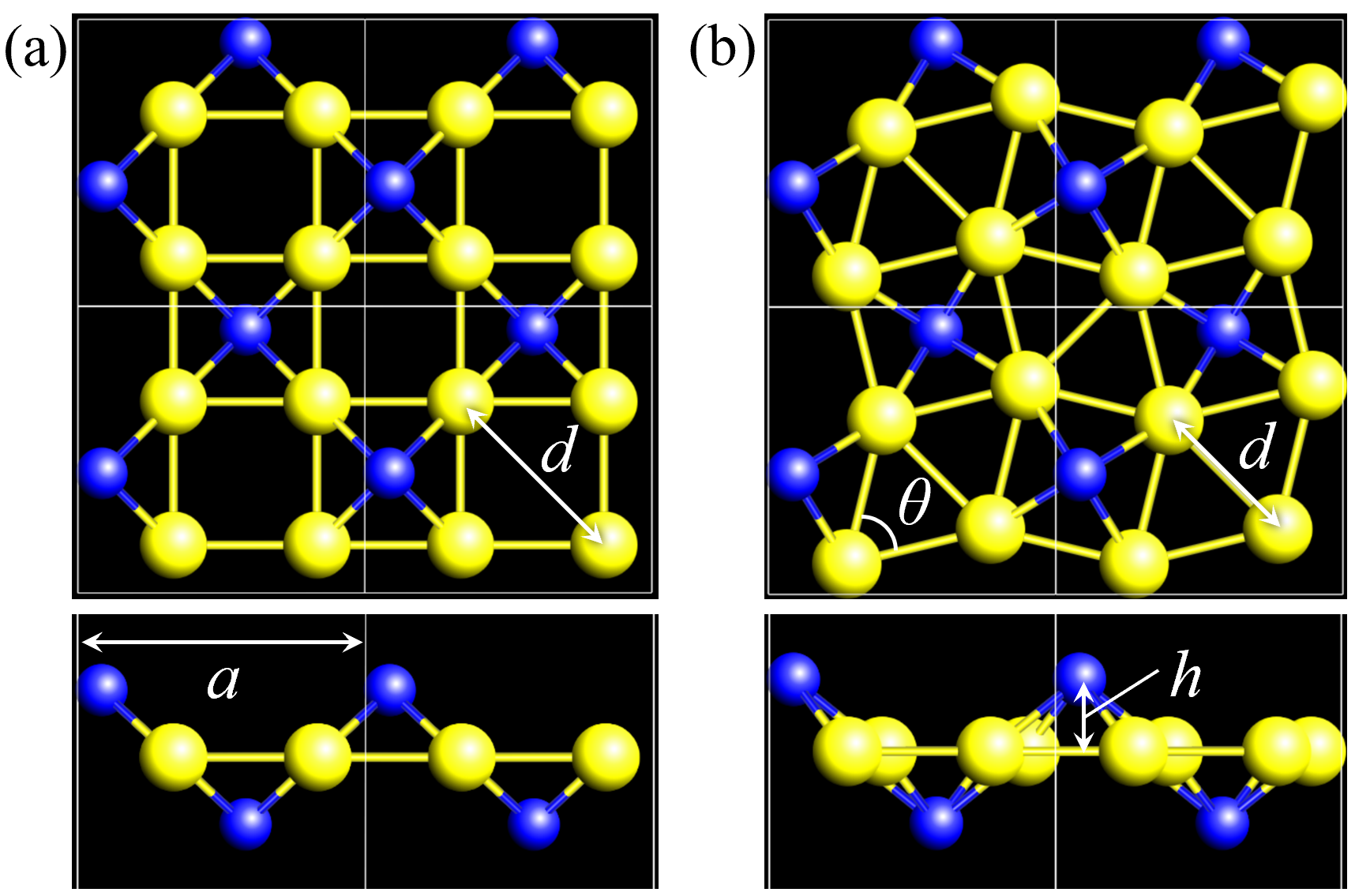
In this work, we discuss how structures (phases) and electronic band structures of Au2S change under strain and adatom substitution, when Au2S is considered as a monolayer consisting of Au lattice networks with S adatoms. For simplicity, Au2S [(90)] and Au2S [(129)] are denoted as buckled--Au2S and buckled--Au2S, or more simply -Au2S and -Au2S, respectively. This paper is organized as follows. In Sec. II, computational details of DFT calculations and phonon calculations are outlined. In Sec. III.1, geometrical structures and stability of - and -Au2S monolayers are discussed with a focus on phase transitions. In Sec. III.2, we focus on the electronic band structures of Au2S, and investigate what the origin of the band gap is and how we can control the band gap. In Sec. IV.1, geometrical structures and stability of - and -Au2X (X=Se, Te, Si, Ge) monolayers are discussed in comparison to those of Au2S. Moreover, as an example of the partially atom-substituted monolayers, we discuss - and -Au4SSe monolayers from the viewpoint of controlling the stability of the phase. The electronic band structures of Au2X monolayers are investigated in Sec. IV.2. The last section is devoted to the conclusions and perspectives.
II Computational details
The first-principles calculations based on DFT were carried out for Au2X (X = S, Se, Te, Si, Ge) type monolayers of - and -phase. The DFT calculations within a generalized gradient approximation (GGA) [12, 13] were performed for the geometry relaxations and variable cell optimizations using the OpenMX code [14] based on norm-conserving pseudopotentials generated with multireference energies [15] and optimized pseudoatomic basis functions [16]. The basis sets we used are listed in Table 1. For example, Au7.0-s3p2d2f1 means that three, two, two, and one optimized radial functions were allocated for the , , , and orbitals, respectively for Au atoms, and the cutoff radius of 7 Bohr was chosen. The qualities of basis functions and fully relativistic pseudopotentials were carefully benchmarked by the delta gauge method [17] to ensure accuracy of our calculations. An electronic temperature of 700 K is used to count the number of electrons by the Fermi-Dirac function. The regular mesh of 240 Ry in real space was used for the numerical integration and for the solution of the Poisson equation [18]. A mesh of k points was adopted. Cell vectors and internal coordinates are simultaneously optimized without any constraint by using a combination scheme of the rational function (RF) method [19] and the direct inversion iterative sub-space (DIIS) method [20] with a BFGS update [21, 22, 23, 24] for the approximate Hessian. The force on each atom was relaxed to be less than 0.0003 Hartree/Bohr. We put four Au atoms and two Si atoms in a square unit cell to form buckled--phase and buckled--phase as initial structures. Calculations of phonon band structures and the density of states (DOS) were carried out by ALAMODE [25]. For the force calculations for estimating force constants, we used supercell structures with 0.04 Å displaced configurations for using a mesh of k points and the regular mesh of about 700 Ry to improve accuracy.
|
III Au2S monolayers
III.1 Structure and stability
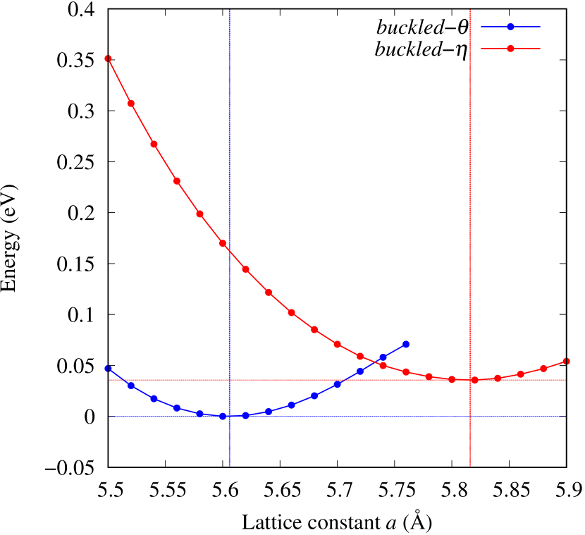
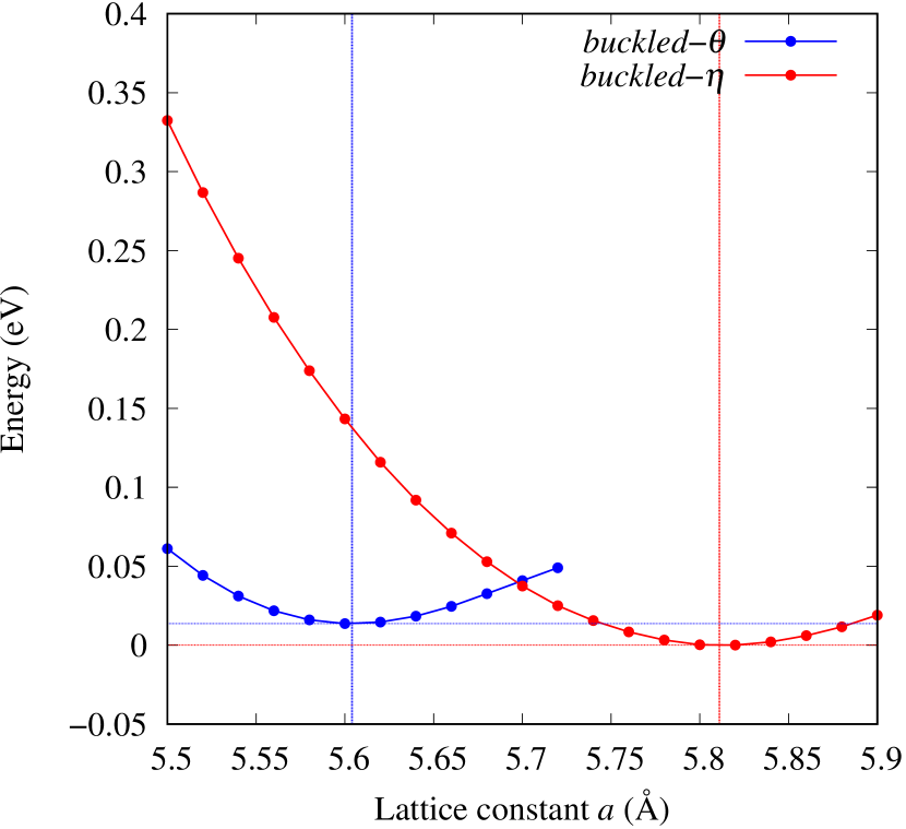
The structures of - and -Au2S monolayers obtained by the geometry optimization are shown in Fig. 1. Four Au atoms in -phase form four square lattice in a unit cell. Two S atoms located Å away from the center of two of the square, either up or down. The height Å of -Au2S is a little bit shorter than Å of -Au2S. In the -Au2S, two squares are distorted, and the distorted angle . Therefore, each distorted square lattice forms two almost equilateral triangles. The lattice constant Å of -Au2S is shorter than Å of -Au2S.
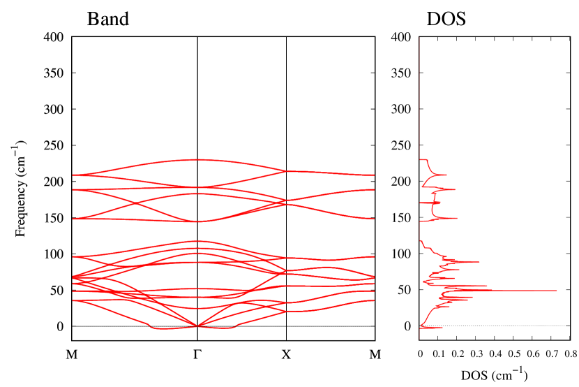
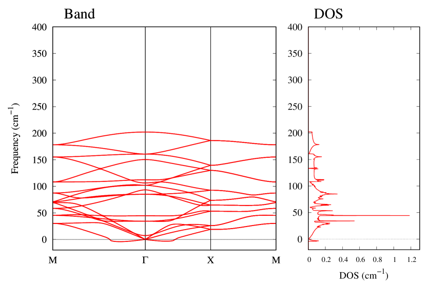
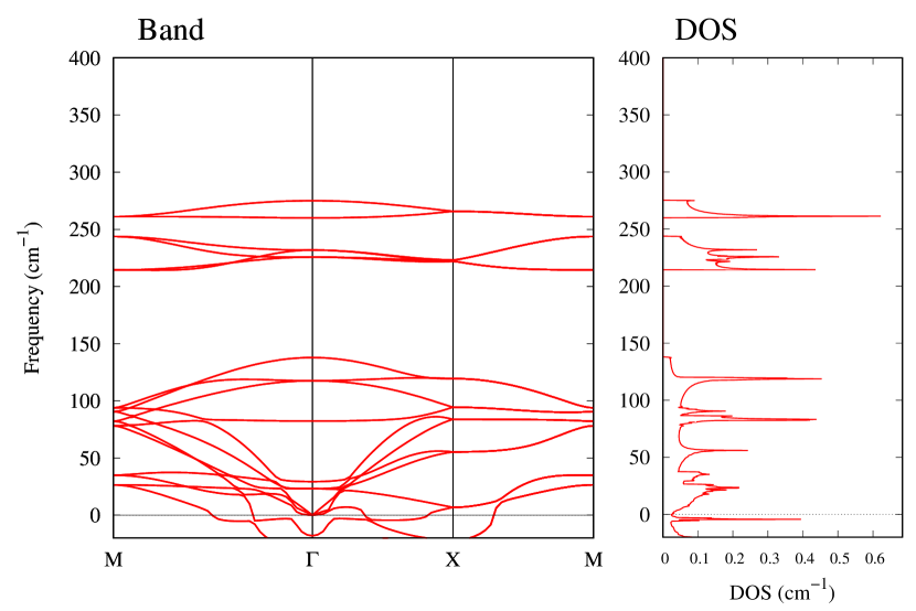
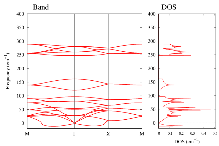
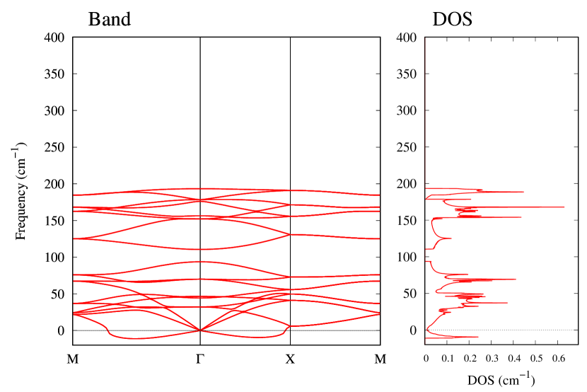
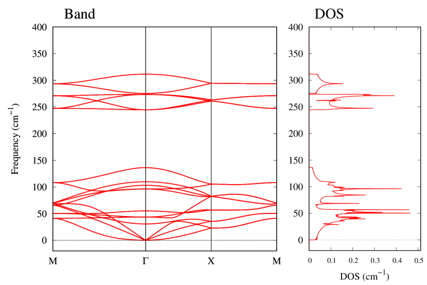
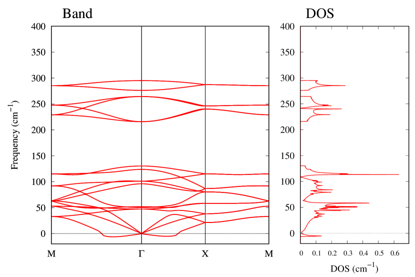
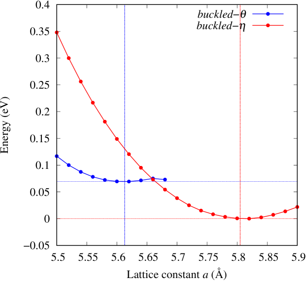
The stability of these Au2S monolayers can be discussed by phonon dispersion and the DOS in Fig. 2. Generally speaking, a negative frequency in a phonon band indicates a negative curvature of the potential energy surface, which means that the structure is unstable or including anharmonic contributions. Therefore, the negative frequency in Fig. 2(b) might indicate the instability or anharmonicity of -Au2S. These phonon bands are consistent with other previous research [8]. In addition, the energy curves for lattice constants in Fig. 3 give us another insight for stability of Au2S. The potential curve of -Au2S is so shallow that a phase transition from -phase to -phase is easily induced by stretching the lattice constants. The opposite concept is also true that the -phase can cause phase transition to the -phase by bi-axial compression to the lattice. Such compression might be induced by lattice matching with a substrate or boundary matching with other monolayers. These kinds of interactions with other stable materials can stabilize unstable monolayers. Silicene on Ag surface [26, 27] and silicene on ZrB2 [28] are good examples for monolayers stabilized on the surface. Therefore, it cannot be said that the -Au2S is sufficiently stable as a free-standing monolayer, but it may be possible to exist on a substrate.
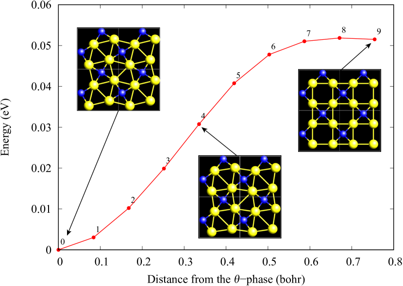
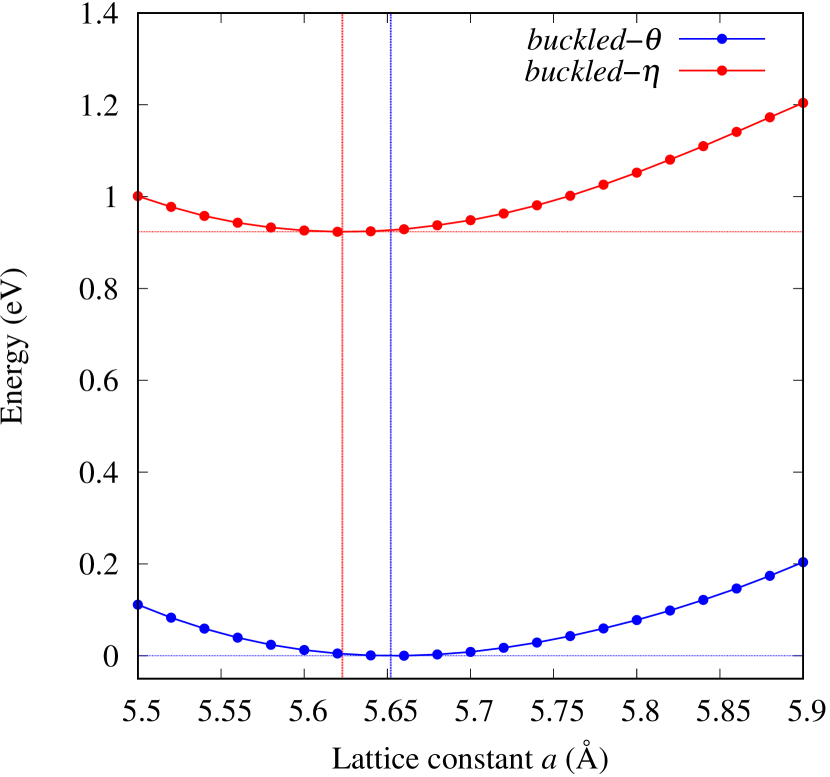
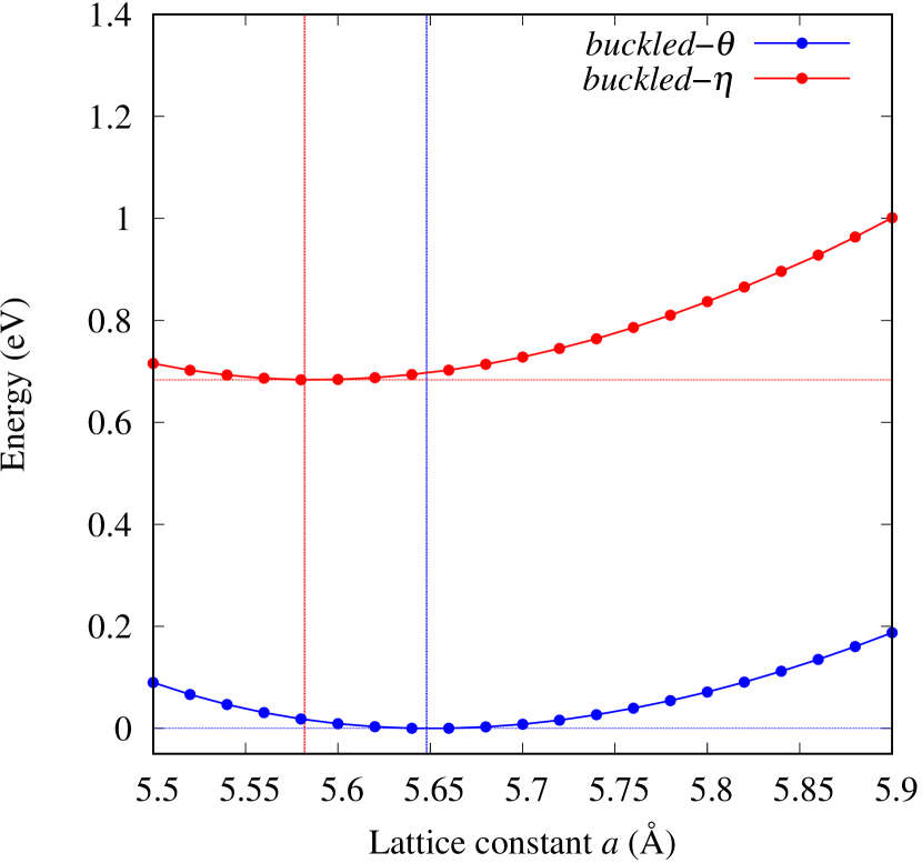
The nudged elastic band (NEB) calculation [29] for Au2S is also performed at the lattice constant Å, which is close to the most stable state of -Au2S. Since the energy barrier from -phase to -phase is very small as shown in Fig. 4, it is concluded that the phase transition of can occur easily by applying the compressive strain of about 3.5% of the lattice constants.
III.2 Electronic band structure
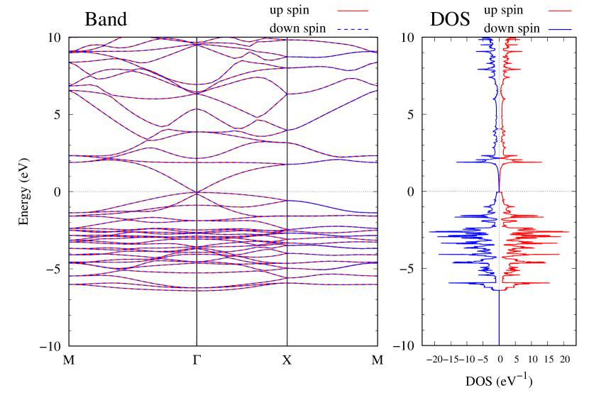
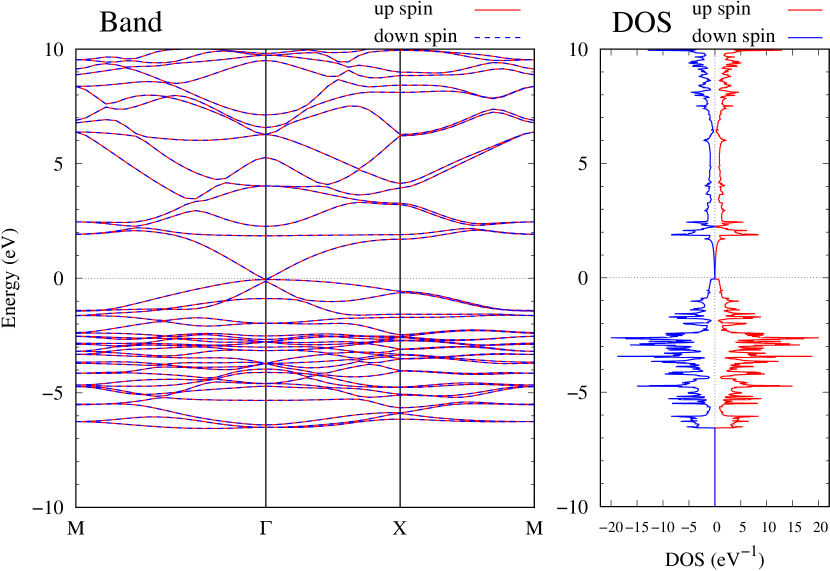
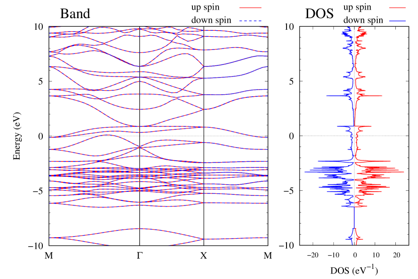
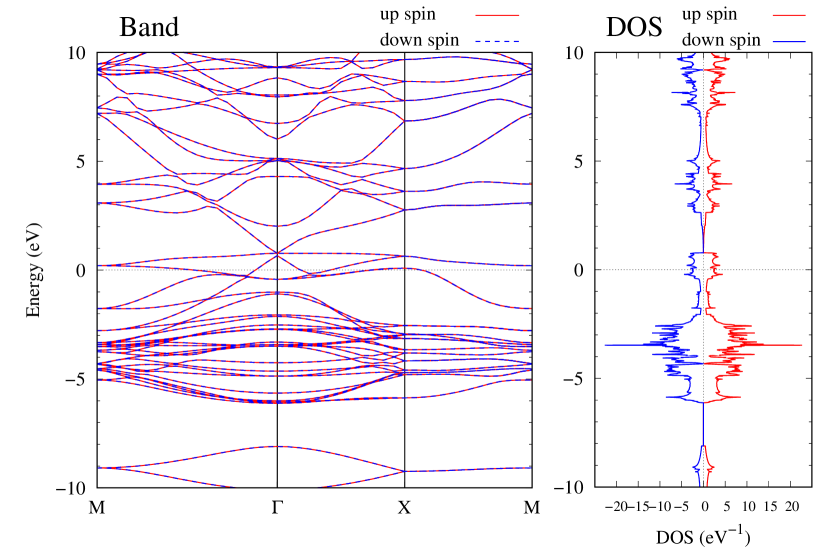
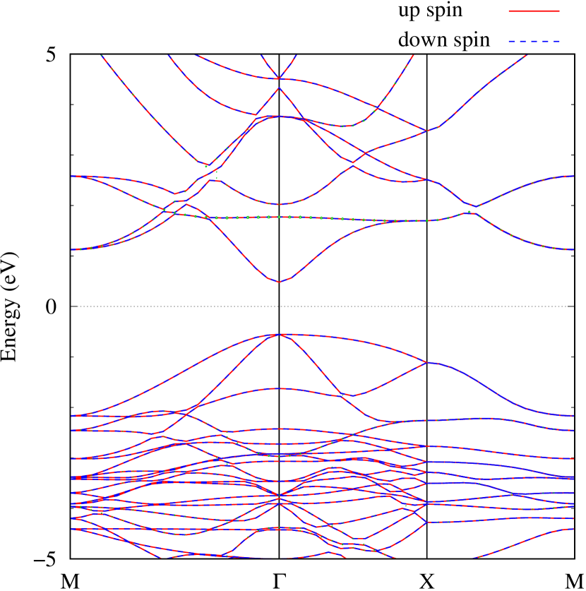
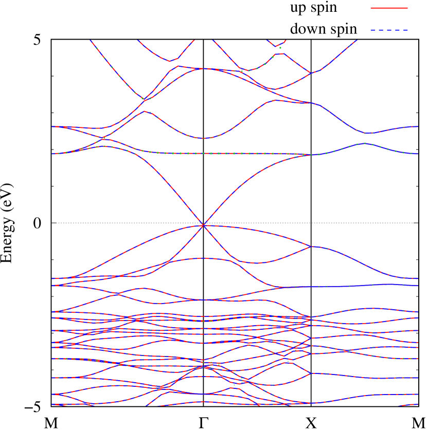
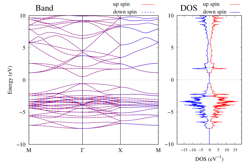
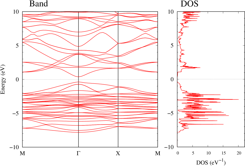
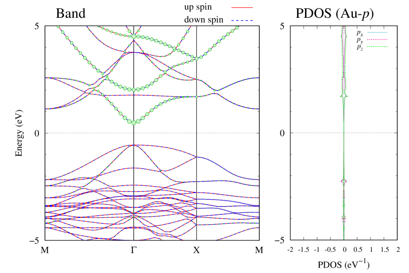
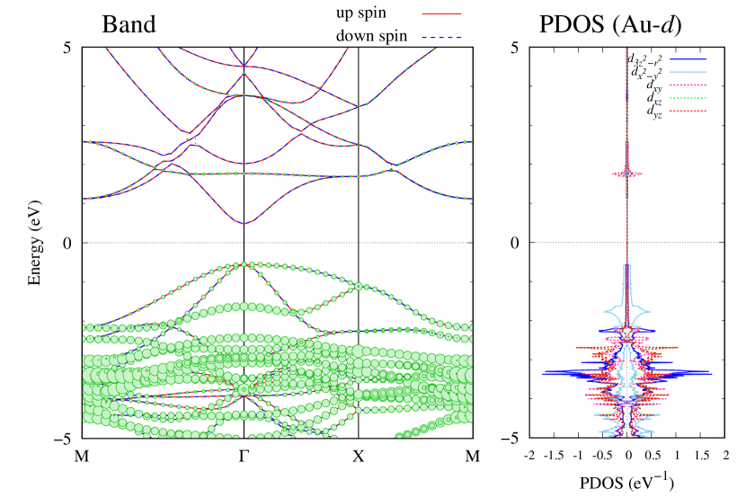
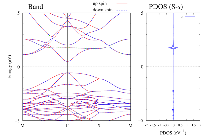
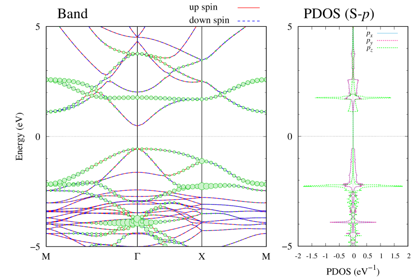
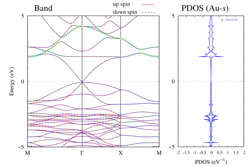
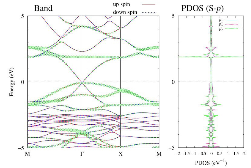
Electronic band structures and the DOS of - and -Au2S monolayers are shown in Figs. 5 (a) and 6 (a). The -Au2S has a direct band gap of 1.02 eV at point, whereas the band gap is closed for the -Au2S. This kind of band gap modulation in the electronic bands of - and -Cu2S by using uniaxial and biaxial stress has been reported previously [30, 8, 11, 10]. In Ref. [11], based on the partial DOS analysis, the researchers have revealed that the valence band maximum (VBM) of -Cu2S is dominantly contributed by the hybridization of , atomic orbitals of S atoms and atomic orbitals of Cu atoms, whereas the conduction band minimum (CBM) of -Cu2S is mainly from the , atomic orbitals of Cu atoms.
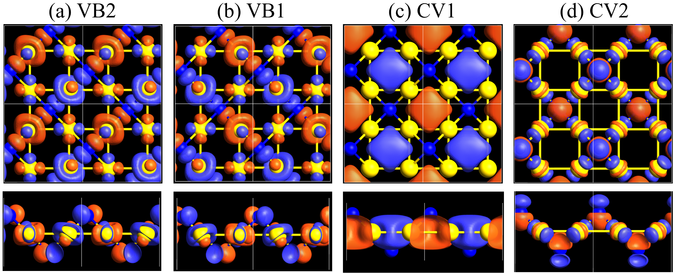
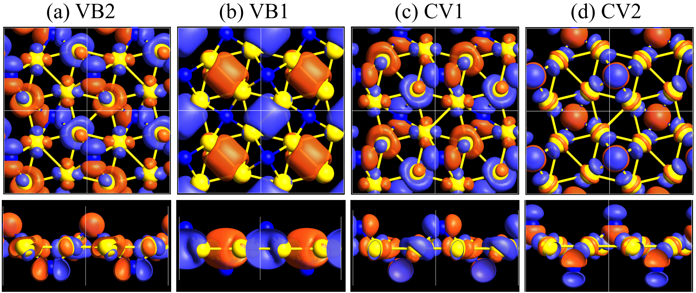
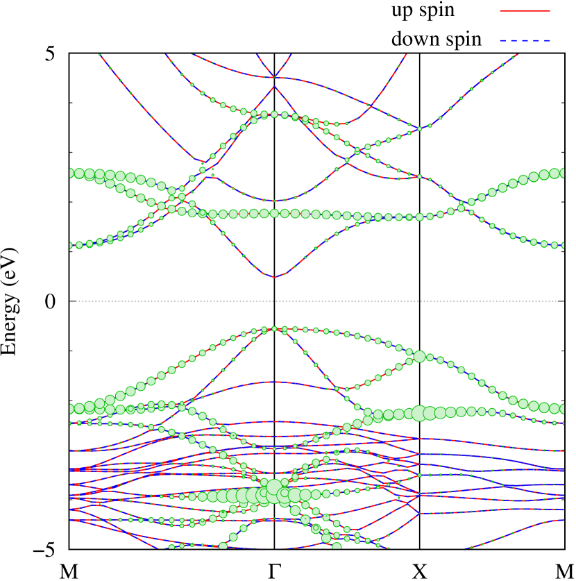
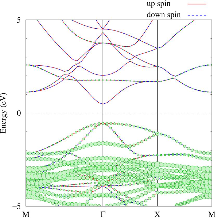
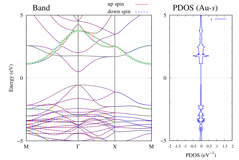
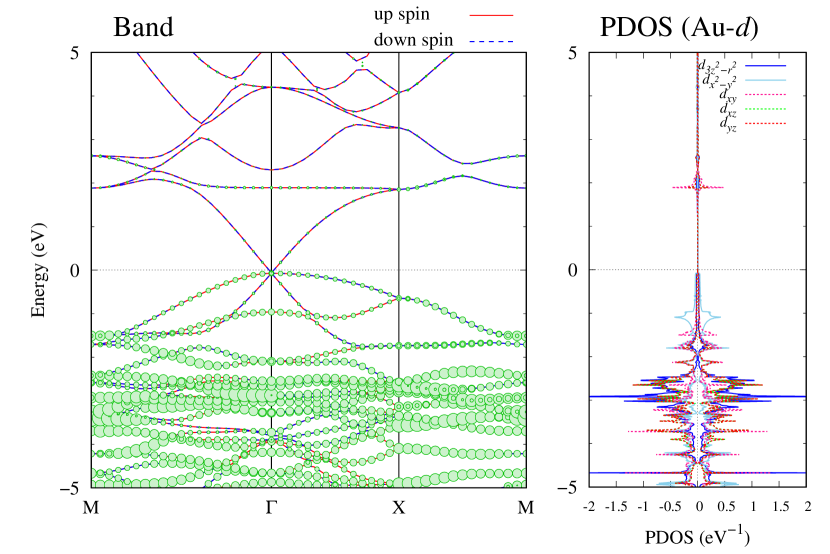
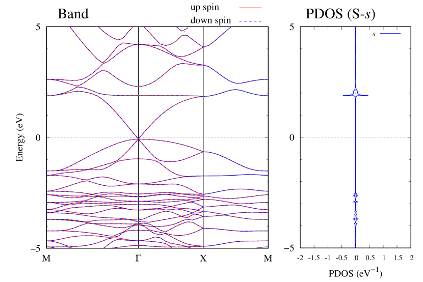
Here, we discuss more details of the origins of the modulations of VBM and CBM around the point. At first, we calculated the weight of each contribution of pseudo-atomic orbital in band structures of - and -Au2S as shown in Figs. 5(b-f) and 6(b-f) based on the Ref. [31]. Additionally, the partial density of states (PDOS) are shown in Figs. S2 and S3 in Supplemental Information. Here, we denote the contribution from type functions of Au atoms as Au-. We also denote the valence (conduction) bands as VB1 (CB1), VB2 (CB2), and so on, in order of proximity to the Fermi level. From Fig. 5 for -Au2S, it is obvious that the VB1 and VB2 have large contributions from both Au- and S-,. In addition, CB1 has contributions from Au-,, forming bonds between Au atoms arranged in a square lattice. In contrast, CB2 have contributions from Au-, and S-, forming a flat band. The shape of VB1 and CB2 of -phase in Fig 6 are similar to those of -phase. However, two bands of VB2 and CB1 of -phase are hybridized and forming a crossing linear dispersion whose main contributions are Au-,, Au-, and S-,. Here, we note that the crossing linear dispersion split a little bit when the spin-orbit interaction is included (see Fig. S1 in Supplemental Information).

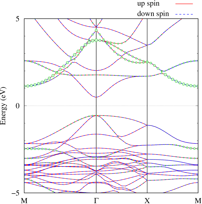
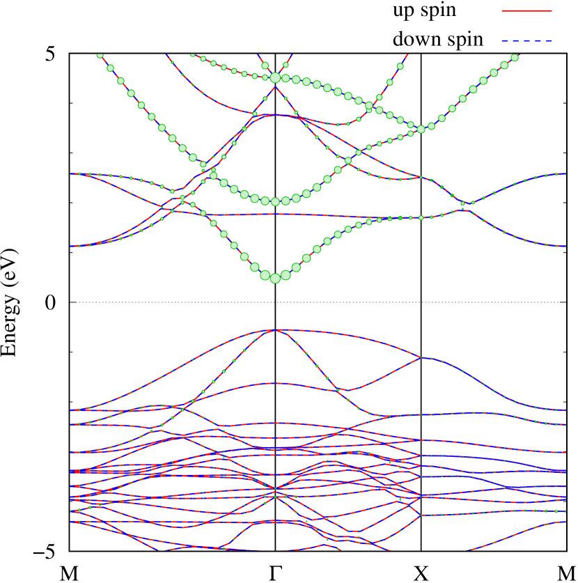


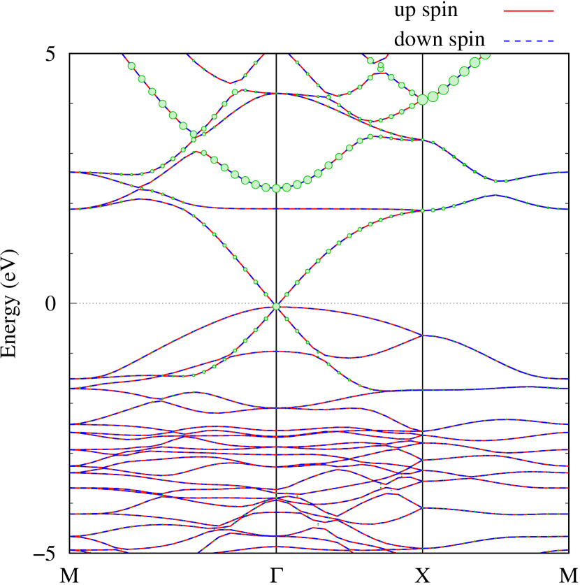
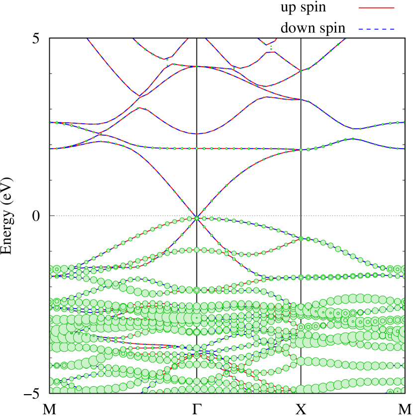
Figures 7 (a) and (b) show band structures of - and -Au2S for various heights ( Å) of S atoms with fixed positions of Au atoms. The band energy of CB1 at the point remains almost unchanged when is varied, since the main contributions of the CB1 are only and of fixed Au atoms. In contrast, the band energies of VB2, VB1 and CB2, including contributions from S atoms, decrease as the S atoms move away from the Au atomic layer. Therefore, it reveals that the CBM depends on the bond distance of Au-Au, not on the interaction between Au and S atoms. On the other hand, the VBM largely depends on the interaction between Au and S atoms. Note that the cases of of -phase are not included in the above discussion to avoid the ambiguity, since the order of the bands is swapped in the cases of of -phase. The flat band, whose energy decreases as is increased, is a band derived from the S- isolation state. It is characteristic that the flatness remains even when is decreased.
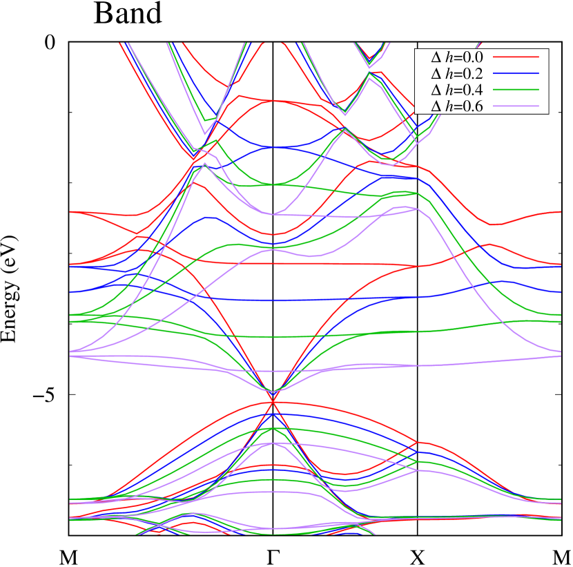
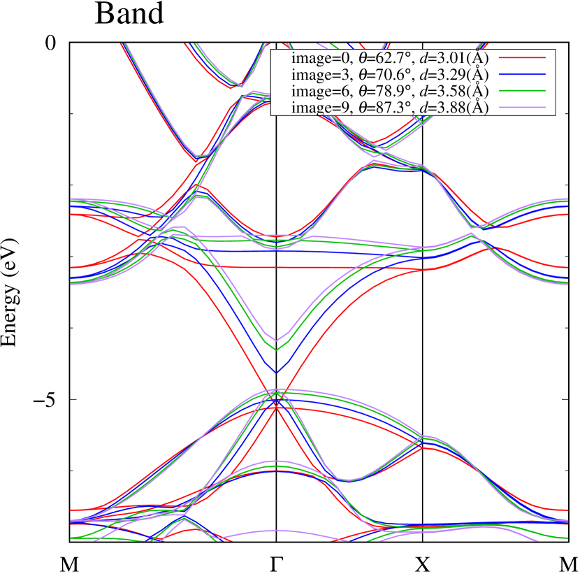
Figure 7(c) shows band structures of transition states from -phase to -phase calculated by using structures obtained by the NEB calculation (Fig. 4). The images 0 and 9 represent the -phase and -phase, respectively. The Au-Au bond distance (see Fig. 1) increases in the transition from -phase to -phase. Moreover, as the Au-Au bond distance increases, the band energy of CB1, which consists of Au-,, increases. Although energies of the other bands, CB2, VB1 and VB2, also increase, the energy shifts are smaller than that of CB1.
To summarize the above discussions on Fig. 7, the CBM can be controlled by the change of Au-Au bond length induced by strain and phase transition, whereas the VBM can be controlled by interaction between the Au layer and attached S atoms.

IV Au2X monolayers
IV.1 Structure and stability
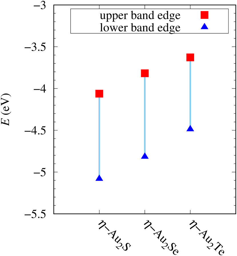
Total energies, cohesive energies, and structural parameters defined in Fig. 1 for - and -Au2X (X=S, Se, Te, Si, Ge), are listed in Table 2. The lattice constants of all the -phase structures in the Table 2 are about 5.6 Å. The lattice constants of the -phase structures are about 5.8 Å for chalcogenides and about 5.6 Å for Si, Ge compounds. This means that lattice constants of these structures are almost independent of the species of atoms attached to the above and below the Au atomic layer. On the other hand, the heights of X atoms are consistent with the trend in the length of the covalent bond radius [32]. Since the angle and the Au-Au bond length defined in Fig. 1 can be measures of the strength of the interaction between Au atoms, Table 2 indicates that -Au2S, -Au2Se and -Au2Te might have stronger Au-Au interactions in that order.
The cohesive energies of monolayers and bulks in Table 2 are defined as
In our results, only - and -Au2S satisfy the condition , which is one of the measures of stability. Therefore, - and -Au2S might be good candidates of stable monolayers. However, it cannot be said that the other monolayers do not exist as a stabilized monolayer, since these kinds of monolayers might be synthesized on a substrate.
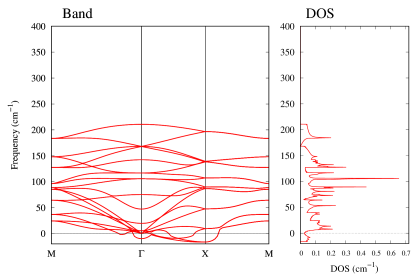
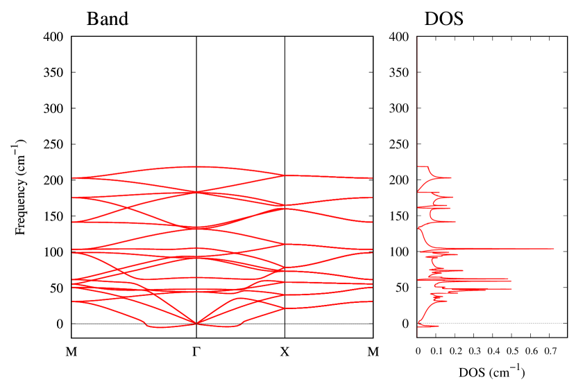
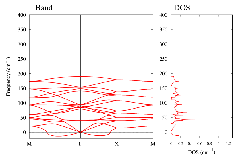
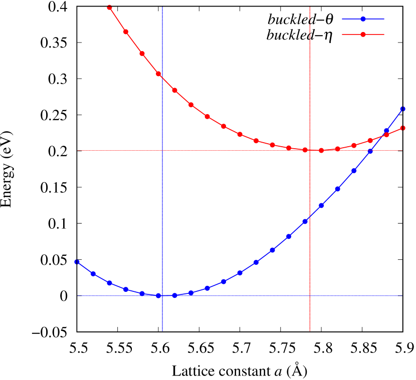
From Figs. S6 and S7 in Supplemental Information, the phonon bands of Au2X monolayers around zero energy have a similar shape to Au2S except for -Au2Si and -Au2Ge, which have large negative frequencies indicating instability. It is also clear from the energy curve in Fig. 8 that Au2Si, Au2Ge, Au2Se, and Au2Te prefer to be -phase, whereas Au2S prefers to be -phase. In other words, the type of more stable phase can be changed by controlling the species of atoms adsorbed on the Au lattice.
As an example of controlling the stability of the phase, we calculated energy curves of - and -Au4SSe, whose structure is generated by replacing a half of S atoms in Au2S to Se atoms, as shown in Fig. 8 (c). The -phase, which is unstable in Au2S, stabilizes and the energy of the most stable state approaches that of the -phase. It means that the phase transition of Au4SSe can be easily induced by tensile and compressive strain of about 3.5% of the lattice constants. Therefore, by partially substituting S atoms, it might be possible to create devices with partially different mechanical and physical properties in a single monolayer.
| Name | (eV) | (Å) | Height (Å) | Angle (deg) | (Å) | ||
|---|---|---|---|---|---|---|---|
| -Au2S | 3.062 | 2.978 | 5.805 | 1.35 | 89.97 | 4.10 | |
| -Au2S | 3.051 | 2.978 | 5.613 | 1.41 | 62.73 | 3.01 | |
| -Au2Se | 2.966 | 3.033 | 5.816 | 1.56 | 90.01 | 4.11 | |
| -Au2Se | 2.972 | 3.033 | 5.606 | 1.61 | 60.72 | 2.93 | |
| -Au2Te | 2.866 | 2.969 | 5.786 | 1.87 | 90.02 | 4.09 | |
| -Au2Te | 2.900 | 2.969 | 5.605 | 1.88 | 58.70 | 2.85 | |
| -Au2Si | 3.111 | 3.723 | 5.623 | 1.54 | 90.03 | 3.98 | |
| -Au2Si | 3.265 | 3.723 | 5.652 | 1.32 | 54.30 | 2.71 | |
| -Au2Ge | 2.940 | 3.418 | 5.582 | 1.76 | 89.97 | 3.95 | |
| -Au2Ge | 3.054 | 3.418 | 5.648 | 1.52 | 54.32 | 2.71 |


IV.2 Electronic band structure
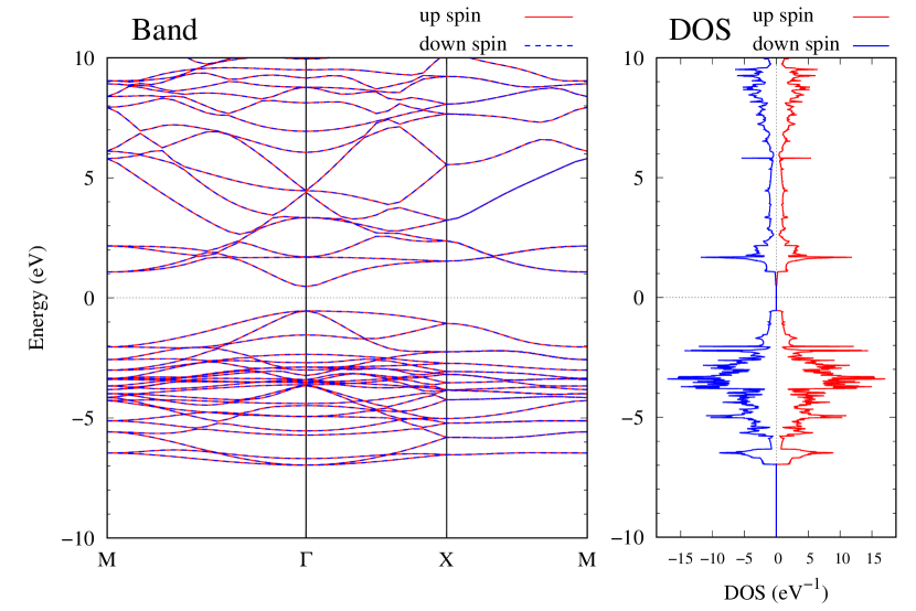
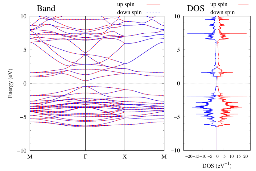
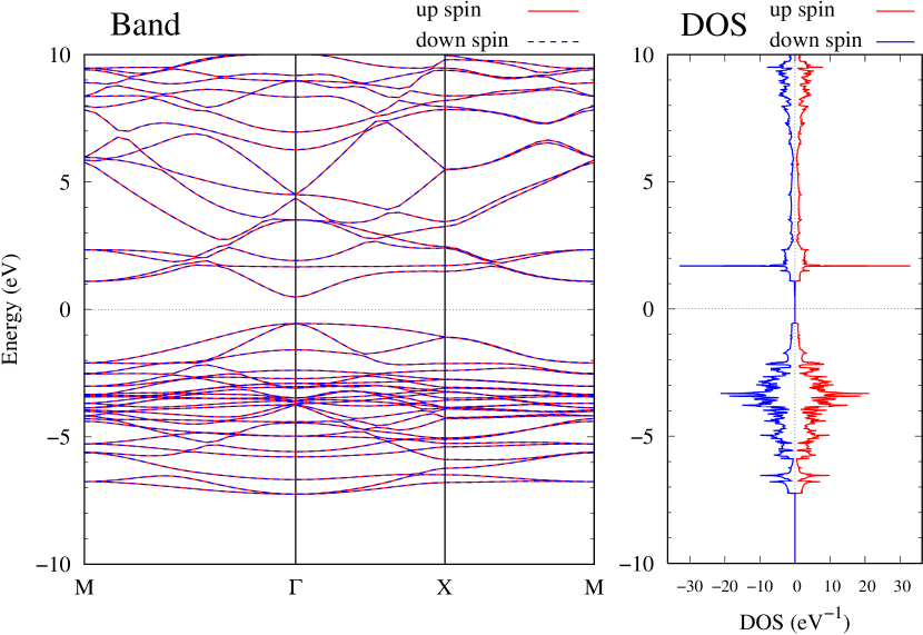
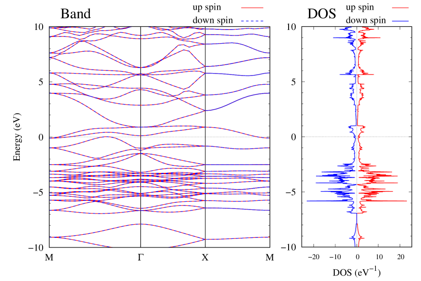
Electronic band structures and the DOSs of -Au2X (X=Se, Te) and - and -Au2Si are shown in Figs. 9 and S10, respectively. The electronic band structures of the other Au2X are shown in the Supplemental Information. The shape of CB2, CB1, VB1, and VB2 of -Au2Se is similar to -Au2S. However, VB2 of -Au2Te is a little bit away from the Fermi level. Therefore, though the band gap of -Au2Te is closing, it does not exist a linear dispersion, which is seen in -Au2S and -Au2Se. The shape of the band structure of -Au2X (X=S, Se, Te) is almost identical, and their band gaps are shown in Fig. 8(f). In contrast, there is no band gap in -Au2Si and -Au2Ge. The shapes of the band structures of - and -Au2Si are totally different from those of Au2X (X=S, Se, Te), since the Fermi level is lower in Au2Si than in Au2S. The linear dispersion and the flat band of -Au2Si on about 0.5 eV at the point have the similar origin to the VB1, VB2 and CB1 of -Au2S. This means that the replacement of X atoms affects the change of the Fermi level, resulting in a drastic change of the band structure.
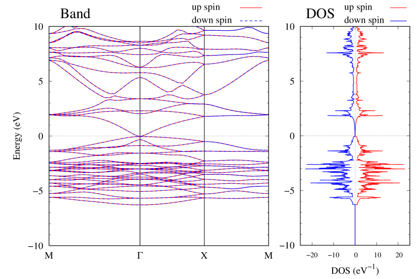
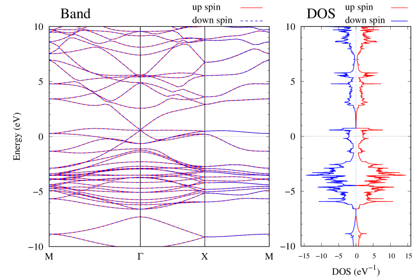
Finally, electronic band structures and the DOSs of - and -Au4SSe, are shown in Fig. 10. The band structure of Au4SSe is almost identical to that of Au2S and Au2Se, since the number of valence electron in Au4SSe is the same as that of Au2S and Au2Se. Therefore, Au4SSe has a band structure similar to Au2S and Au2Se, and is equally stable in the - and -phases.


V Conclusions and perspectives
In this paper, we have analyzed the phase transition and the change of electronic band structures of Au2S induced by strain. We have pointed out that about 3.5% compressive biaxial strain on -Au2S, which is induced, e.g., by lattice matching with a substrate, can cause a transition to -Au2S. It has also shown that the direct band gap of 1.02 eV in -Au2S disappears by this phase transition. Therefore, it has revealed that the band gap and the phase of Au2S can be controlled by strain. In addition, we have investigated the origin of band modulations around the point. We have concluded that the band energy of CB1, which corresponds to CBM, is independent of the interaction between Au and S atoms, while the increase of the Au-Au bond distance contributes significantly to the increase of the band energy of CB1. We also have found that the band energy of VB1, which corresponds to VBM, depends on both Au-S and Au-Au interactions. In particular, the band energy of VB1 decreases as the interaction between Au atoms and S atoms decreases. In the -Au2S, CB1 and VB2 intersect on the point, creating linear dispersion. These perspectives are significant for band gap engineering.
In the latter section, we have investigated - and -Au2X (X=Se, Te, Si, Ge) and Au4SSe. Au2Se and Au2Te differ from Au2S in that the -phase is more stable than the -phase, although the electronic band structures are similar to those of Au2S. The energy curve of Au4SSe has revealed that we can modify the electronic state to be equally stable in the and phases by replacing some of the S atoms to Se atoms. The electronic band structure of Au2Si have revealed that the Fermi level can be shifted by replacing S atoms with Si atoms, which have different valence electron numbers, resulting in changing from semiconductor to metal. This means that, by replacing S atoms in a part of -Au2S that we want to give conductivity with other atoms, electronic circuits can be constructed on a single monolayer.
Thus, this family of Au2X type monolayers has a potential to acquire a diversity of physical quantities by replacing the X element without breaking the basic Au lattice network. The family of Au2X type monolayers may be a candidate of materials of atomic scale network devices.
VI Acknowledgement
The computation in this work has been done using the facilities of the Supercomputer Center, the Institute for Solid State Physics, the University of Tokyo. The authors acknowledge financial support from JSPS KAKENHI Grant Number 20H00328.
References
- Ashton et al. [2017] M. Ashton, J. Paul, S. B. Sinnott, and R. G. Hennig, Topology-scaling identification of layered solids and stable exfoliated 2d materials, Phys. Rev. Lett. 118, 106101 (2017).
- Haastrup et al. [2018] S. Haastrup, M. Strange, M. Pandey, T. Deilmann, P. S. Schmidt, N. F. Hinsche, M. N. Gjerding, D. Torelli, P. M. Larsen, A. C. Riis-Jensen, J. Gath, K. W. Jacobsen, J. J. Mortensen, T. Olsen, and K. S. Thygesen, The computational 2d materials database: high-throughput modeling and discovery of atomically thin crystals, 2D Materials 5, 042002 (2018).
- Zhou et al. [2018] J. Zhou, J. Lin, X. Huang, Y. Zhou, Y. Chen, J. Xia, H. Wang, Y. Xie, H. Yu, J. Lei, D. Wu, F. Liu, Q. Fu, Q. Zeng, C.-H. Hsu, C. Yang, L. Lu, T. Yu, Z. Shen, H. Lin, B. I. Yakobson, Q. Liu, K. Suenaga, G. Liu, and Z. Liu, A library of atomically thin metal chalcogenides, Nature 556, 355 (2018).
- Fukuda et al. [2021] M. Fukuda, J. Zhang, Y.-T. Lee, and T. Ozaki, A structure map for ab2 type 2d materials using high-throughput dft calculations, Mater. Adv. 2, 4392 (2021).
- AB [2] Our AB2 structure map and database are available on the interactive website: www.openmx-square.org/2d-ab2/.
- Oyedele et al. [2017] A. D. Oyedele, S. Yang, L. Liang, A. A. Puretzky, K. Wang, J. Zhang, P. Yu, P. R. Pudasaini, A. W. Ghosh, Z. Liu, C. M. Rouleau, B. G. Sumpter, M. F. Chisholm, W. Zhou, P. D. Rack, D. B. Geohegan, and K. Xiao, Pdse2: Pentagonal two-dimensional layers with high air stability for electronics, Journal of the American Chemical Society 139, 14090 (2017), pMID: 28873294, https://doi.org/10.1021/jacs.7b04865 .
- Taheri et al. [2022] A. Taheri, S. Pisana, and C. V. Singh, Extraordinary lattice thermal conductivity of gold sulfide monolayers, Nanoscale Adv. 4, 2873 (2022).
- Gao et al. [2021] L. Gao, Y.-F. Zhang, and S. Du, Semiconducting m2x (m = cu, ag, au; x = s, se, te) monolayers: A broad range of band gaps and high carrier mobilities, Nano Research 14, 2826 (2021).
- Wu et al. [2019] Q. Wu, W. W. Xu, D. Lin, J. Wang, and X. C. Zeng, Two-dimensional gold sulfide monolayers with direct band gap and ultrahigh electron mobility, The Journal of Physical Chemistry Letters 10, 3773 (2019), pMID: 31244267, https://doi.org/10.1021/acs.jpclett.9b01312 .
- Zhu et al. [2019] H. Zhu, S. Li, W. Xia, Y. Wang, and L. Shi, Bandgap engineering of strained monolayer semiconductor cu2s and its outstanding mechanical flexibility, Solid State Communications 302, 113704 (2019).
- Chen et al. [2020] X. Chen, D. Wang, X. Liu, L. Li, and B. Sanyal, Two-dimensional square-a2b (a = cu, ag, au, and b = s, se): Auxetic semiconductors with high carrier mobilities and unusually low lattice thermal conductivities, The Journal of Physical Chemistry Letters 11, 2925 (2020), pMID: 32223172, https://doi.org/10.1021/acs.jpclett.0c00613 .
- Kohn and Sham [1965] W. Kohn and L. J. Sham, Self-consistent equations including exchange and correlation effects, Phys. Rev. 140, A1133 (1965).
- Perdew et al. [1996] J. P. Perdew, K. Burke, and M. Ernzerhof, Generalized gradient approximation made simple, Phys. Rev. Lett. 77, 3865 (1996).
- [14] T. Ozaki et al., OpenMX package.
- Morrison et al. [1993] I. Morrison, D. M. Bylander, and L. Kleinman, Nonlocal hermitian norm-conserving vanderbilt pseudopotential, Phys. Rev. B 47, 6728 (1993).
- Ozaki [2003] T. Ozaki, Variationally optimized atomic orbitals for large-scale electronic structures, Phys. Rev. B 67, 155108 (2003).
- Lejaeghere et al. [2016] K. Lejaeghere, G. Bihlmayer, T. Björkman, P. Blaha, S. Blügel, V. Blum, D. Caliste, I. E. Castelli, S. J. Clark, A. Dal Corso, S. de Gironcoli, T. Deutsch, J. K. Dewhurst, I. Di Marco, C. Draxl, M. Dułak, O. Eriksson, J. A. Flores-Livas, K. F. Garrity, L. Genovese, P. Giannozzi, M. Giantomassi, S. Goedecker, X. Gonze, O. Grånäs, E. K. U. Gross, A. Gulans, F. Gygi, D. R. Hamann, P. J. Hasnip, N. A. W. Holzwarth, D. Iuşan, D. B. Jochym, F. Jollet, D. Jones, G. Kresse, K. Koepernik, E. Küçükbenli, Y. O. Kvashnin, I. L. M. Locht, S. Lubeck, M. Marsman, N. Marzari, U. Nitzsche, L. Nordström, T. Ozaki, L. Paulatto, C. J. Pickard, W. Poelmans, M. I. J. Probert, K. Refson, M. Richter, G.-M. Rignanese, S. Saha, M. Scheffler, M. Schlipf, K. Schwarz, S. Sharma, F. Tavazza, P. Thunström, A. Tkatchenko, M. Torrent, D. Vanderbilt, M. J. van Setten, V. Van Speybroeck, J. M. Wills, J. R. Yates, G.-X. Zhang, and S. Cottenier, Reproducibility in density functional theory calculations of solids, Science 351, aad3000 (2016).
- Ozaki and Kino [2005] T. Ozaki and H. Kino, Efficient projector expansion for the ab initio lcao method, Phys. Rev. B 72, 045121 (2005).
- Banerjee et al. [1985] A. Banerjee, N. Adams, J. Simons, and R. Shepard, Search for stationary points on surfaces, The Journal of Physical Chemistry 89, 52 (1985), https://doi.org/10.1021/j100247a015 .
- Csaszar and Pulay [1984] P. Csaszar and P. Pulay, Geometry optimization by direct inversion in the iterative subspace, Journal of Molecular Structure 114, 31 (1984).
- BROYDEN [1970] C. G. BROYDEN, The Convergence of a Class of Double-rank Minimization Algorithms 1. General Considerations, IMA Journal of Applied Mathematics 6, 76 (1970).
- Fletcher [1970] R. Fletcher, A new approach to variable metric algorithms, The Computer Journal 13, 317 (1970).
- Goldfarb [1970] D. Goldfarb, A family of variable-metric methods derived by variational means, Mathematics of Computation 24, 23 (1970).
- Shanno [1970] D. F. Shanno, Conditioning of quasi-newton methods for function minimization, Mathematics of Computation 24, 647 (1970).
- Tadano et al. [2014] T. Tadano, Y. Gohda, and S. Tsuneyuki, Anharmonic force constants extracted from first-principles molecular dynamics: applications to heat transfer simulations, Journal of Physics: Condensed Matter 26, 225402 (2014).
- Gao and Zhao [2012] J. Gao and J. Zhao, Initial geometries, interaction mechanism and high stability of silicene on ag(111) surface, Scientific Reports 2, 861 (2012).
- Feng et al. [2018] L. Feng, K. Yabuoshi, Y. Sugimoto, J. Onoda, M. Fukuda, and T. Ozaki, Structural identification of silicene on the ag(111) surface by atomic force microscopy, Phys. Rev. B 98, 195311 (2018).
- Fleurence et al. [2012] A. Fleurence, R. Friedlein, T. Ozaki, H. Kawai, Y. Wang, and Y. Yamada-Takamura, Experimental evidence for epitaxial silicene on diboride thin films, Phys. Rev. Lett. 108, 245501 (2012).
- Henkelman and Jonsson [2000] G. Henkelman and H. Jonsson, Improved tangent estimate in the nudged elastic band method for finding minimum energy paths and saddle points, The Journal of Chemical Physics 113, 9978 (2000), https://pubs.aip.org/aip/jcp/article-pdf/113/22/9978/10828773/9978_1_online.pdf .
- Guo et al. [2019] Y. Guo, Q. Wu, Y. Li, N. Lu, K. Mao, Y. Bai, J. Zhao, J. Wang, and X. C. Zeng, Copper(i) sulfide: a two-dimensional semiconductor with superior oxidation resistance and high carrier mobility, Nanoscale Horiz. 4, 223 (2019).
- Lee et al. [2013] C.-C. Lee, Y. Yamada-Takamura, and T. Ozaki, Unfolding method for first-principles LCAO electronic structure calculations, J. Phys. Condens. Matter 25, 345501 (2013).
- Pyykkö and Atsumi [2009] P. Pyykkö and M. Atsumi, Molecular single-bond covalent radii for elements 1–118, Chemistry - A European Journal 15, 186 (2009).
Supplemental Information


| Band | Function Types |
|---|---|
| CB2 | Au-,, S- |
| CB1 | Au-, |
| VB1 | Au-, S-, |
| VB2 | Au-, S-, |