Generation of imprinted strain gradients for spintronics
Abstract
In this work, we propose and evaluate an inexpensive and CMOS-compatible method to locally apply strain on a Si/SiOx substrate. Due to high growth temperatures and different thermal expansion coefficients, a SiN passivation layer exerts a compressive stress when deposited on a commercial silicon wafer. Removing selected areas of the passivation layer alters the strain on the micrometer range, leading to changes in the local magnetic anisotropy of a magnetic material through magnetoelastic interactions. Using Kerr microscopy, we experimentally demonstrate how the magnetoelastic energy landscape, created by a pair of openings, in a magnetic nanowire enables the creation of pinning sites for in-plane vortex walls that propagate in a magnetic racetrack. We report substantial pinning fields up to 15 mT for device-relevant ferromagnetic materials with positive magnetostriction. We support our experimental results with finite element simulations for the induced strain, micromagnetic simulations and 1D model calculations using the realistic strain profile to identify the depinning mechanism. All the observations above are due to the magnetoelastic energy contribution in the system, which creates local energy minima for the domain wall at the desired location. By controlling domain walls with strain, we realize the prototype of a true power-on magnetic sensor that can measure discrete magnetic fields or Oersted currents. This utilizes a technology that does not require piezoelectric substrates or high-resolution lithography, thus enabling wafer-level production.
One of the promising "Beyond COMS" technologies are nanomagnetic and spintronic devices due to their non-volatile nature, high operating speed, extremely low power consumption, and well explored routes to read and write dataManipatruni, Nikonov, and Young (2018). One example is nanomagnetic tracks, where information (stored in domain walls - DWs) is propagated and manipulated by dipolar interaction along soft ferromagnetic nanowiresOno et al. (1999); Atkinson et al. (2003). The manipulation of DWs has quite a long history and a turning point in this research area was the demonstration of a current-controlled magnetic DW shift register Hayashi et al. (2008); Kumar et al. (2022) (racetrack memory). Since then, more work has been done on the development of DW-based memoriesFranken, Swagten, and Koopmans (2012), logic devicesLuo et al. (2020) and sensorsZhang et al. (2018); Diegel et al. (2009); Khan et al. (2021); Borie et al. (2017) or neuromorphic computingAlamdar et al. (2021); Yue et al. (2019). However, feasibility of the fabrication process and compatibility with existing CMOS devices must be ensured before full technological realization is achieved.
One of the key challenges with these devices is the control of DWsBoulle, Malinowski, and Kläui (2011), typically realized using geometric constraints (notches) Omari et al. (2019); Shiu et al. (2021); Al Bahri et al. (2019) or the local manipulation of the magnetic anisotropy through strain Fattouhi et al. (2022); Masciocchi et al. (2021) using magnetostrictive/piezoelectric systems Lei et al. (2013); Zhou et al. (2020); Hu et al. (2016); Dean et al. (2011). However, these approaches are not attractive for most sensor manufacturers due to high cost and complexity. Respectively, because high-resolution notches and presence of the multiferroic stack would require significant investments in tools for high-resolution lithography and layer deposition. Also, the presence of voltages for piezoelectric actuation via metallic contacts increases design complexity and area usage. It is moreover difficult to realize an arbitrary shape of strain and strain gradients down to the micrometer range with piezoelectric substrates because it is technologically nontrivial to confine the electric fieldsBarra et al. (2021).
An alternative method of transferring strain to a thin filmChu et al. (2009); Doherty et al. (2020), is the use of capping layers Martin et al. (2009) widely used in the semiconductor and photovoltaic industries because they provide protection from hostile environments.
In this work, we propose and experimentally demonstrate a low-cost and CMOS-compatible method to induce local strain on a Si/SiOx substrate by removing selected regions of the passivation layer. Arbitrary strain magnitudes and strain gradients can be realized by simply choosing the design of the removed part. The magnitude and profile of the strain are determined by combining anisotropy and stress measurements with finite elements simulations. We experimentally demonstrate, using Kerr microscopy, that this local strain allows for domain wall pinning in a racetrack element. This is verified by micromagnetic simulations and 1D model calculations. Finally, to show the technological relevance of this method, we propose and verify a non-volatile magnetic peak-field sensor based on this technology.
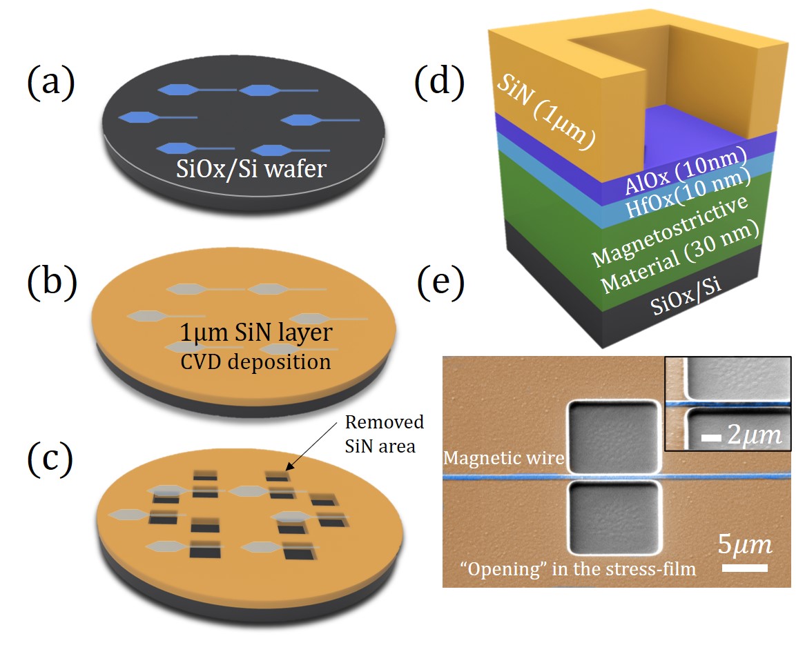
Samples of AlOx(10 nm)/HfOx(10)/Co70Fe30(30) and AlOx(10 nm)/HfOx(10)/Co40Fe40B20(30) were prepared by DC magnetron sputtering using a Singulus Rotaris system on a SiOx(1.5 µm)/Si(625 µm) substrate. Using optical lithography and etching, nanowires were fabricated with a variable width - between 800 and 500 nm - and a length of 70 µm. A reservoir at the left end allows for DWs injection at lower fields. After the first lithography step, the wafer was covered with a 1 µm thick SiN layer using plasma-enhanced chemical vapor deposition (PECVD) at a temperature of 250∘C. The residual stress on the wafer is quantified using a standard wafer bow measurement. A second optical lithography step is used in combination with reactive ion etching (RIE) to remove selected areas (up to µm2) of the SiN layer (openings) without damaging the magnetic layer, as shown in Figs.1 (a) - (d) while the wafer surface is still largely covered. The hysteresis loops of the thin films are measured using a BH-looper with a setup to measure magnetostriction. The magneto-optic Kerr effect (MOKE) was used to image the magnetization state in the devicesMcCord (2015); Soldatov and Schäfer (2017).
To understand the origin of the intrinsic stress in our system, one should consider the coefficients of thermal expansion of a film and a substrate, along with the high temperature during deposition. If the thermal expansion coefficients are different, thermal stresses arise when the whole stack cools down to room temperature after deposition Ohring (1992). Relaxation of this stress leads to a deformation, i.e. bending, of the wafer (Figs. 1(a)-(b)) allowing for the residual stress to be estimatedMarks, Hassan, and Cheong (2014). The measured in-plane (compressive) stress is planar and in our case has a magnitude of MPa. To create a non-uniform stress on the substrate surface, selected areas of the SiN are completely removed, creating some openings in the passivation layer (Fig. 1 (c)). The etching is monitored to stop the process at the AlOx/SiN interface, as shown in Fig. 1 (d), so that the integrity of the magnetic layer is preserved. An example of the final device is shown in a scanning electron microscopy image (SEM) in Fig. 1 (e) for a pair of square apertures µm2 in size. With a suitable lithography mask, arbitrary shapes, sizes, and spacing of the apertures can be realized with sub µm resolution. In the example presented here, the openings are spaced 1 µm apart and the 800 nm wide magnetic track under the SiN layer shows no signs of damage caused by the etching process.
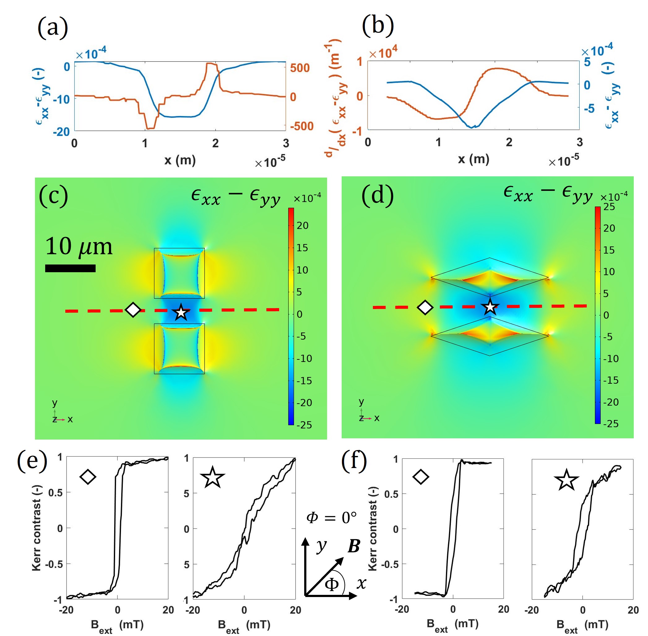
To determine the magnitude of stress relieved, finite-element-method (FEM) simulations were performed using the COMSOL Multiphysics® Structural Mechanics ModuleCOMSOL AB, Stockholm, Sweden (2023). More details about FEM simulations can be found in Section S1 of the supplementary material. To have a well defined strained region in racetrack type devices, it is convenient to consider a pair of openings - to be realized at each side of a magnetic nanowire. Figs. 2 (a) - (d) contain the computed values of the surface strain at the interface between SiN/SiOx for two different opening geometries. As shown in Figs. 2 (c) and (d), the effective surface strain is close to zero at a distance greater than 20 µm from the etched areas and becomes non-uniform in their proximity. The geometry of the opening determines the strain profile. This can be seen in Figs. 2 (a) and (b) where the effective strain is plotted along the dashed line running between the two openings shown in Figs. 2 (c) and (d), respectively. For a square pair of openings (Fig. 2 (a)), the effective uniaxial strain profile is mostly flat and confined between them with strain gradient maxima (minima) at the exit (entrance) of the strained area. The strain reaches values of . For a diamond shaped pair of openings, the strain is again confined between the openings but its magnitude increases almost linearly towards the center. This time the strain gradient is mostly constant.
To experimentally confirm the magnitude and sign of this local strain, we measured the magnetization curves of a unpatterned film of AlOx/HfOx/Co70Fe30 (30 nm) underneath the patterned SiN. The hysteresis loops were measured with field applied along at different locations on the sample, selecting a region of interest of µm2 size within the field of view of the Kerr microscope. Full angular dependence of the anisotropy is reported in section S3 of the supplementary information. Since Co70Fe30 has considerable magnetostriction (), the strain acting on the film is coupled to the magnetization via the magnetoelastic effect, as expressed in the anisotropy energyFinizio et al. (2014)
| (1) |
where is the Young’s modulus and is the saturation magnetostriction. As done in previous works Masciocchi et al. (2021, 2022) the in-plane magnetoelastic anisotropy can be locally estimated. Measuring hysteresis loops, where an in-plane field is applied along two perpendicular directions, can give us a direct measurement of the local strainMcCord (2004); Urs et al. (2014); Thórarinsdóttir et al. (2022).
In Figs. 2 (e) - (f) hysteresis loops of an unpatterned film, this time of SiN/AlOx/HfOx/Co70Fe30(30 nm), are shown. The openings geometry is the one of Figs. 2 (c) - (d), respectively. Looking at Fig. 2 (e) we can compare the magnetization curve before (diamond) and between (star) the square openings. The anisotropy field increases, due to (uniaxial) magnetoelastic anisotropy. As Co70Fe30 has a positive magnetostriction, the increase in anisotropy field ( kJ/m3) is caused by a negative (compressive) strain, in agreement with our FEM simulation. Using Eq. 1 and the values of magnetoelastic anisotropy difference we can estimate the strain to be for a square opening of this size. The same measurement can be performed for a diamond-shaped pair of openings and is reported in Fig. 2 (f). The calculated maximum strain difference for this case is .
The strain, created by removing specific areas of the SiN layer could be used as a mechanism to move, change direction, or stop a DW, a feature often needed in the device implementationMasciocchi et al. (2021); Diegel et al. (2009). Typical ways to do so relies on the modification of the DW energy making it a spatially variable quantity. In analogy with the conventional field-driven case, the magnetoelastic field can be considered as a force that pushes the DW along the direction of decreasing energy, i.e., increasing compressive strain if for the in-plane-strain-gradient case. This force is proportional to the local gradient of the spatially variable quantity Wen et al. (2020); Fattouhi et al. (2022, 2021), and its effect is essentially that of an effective (magnetoelastic) field
| (2) |
where is the magnetoelastic DW energy per unit area.
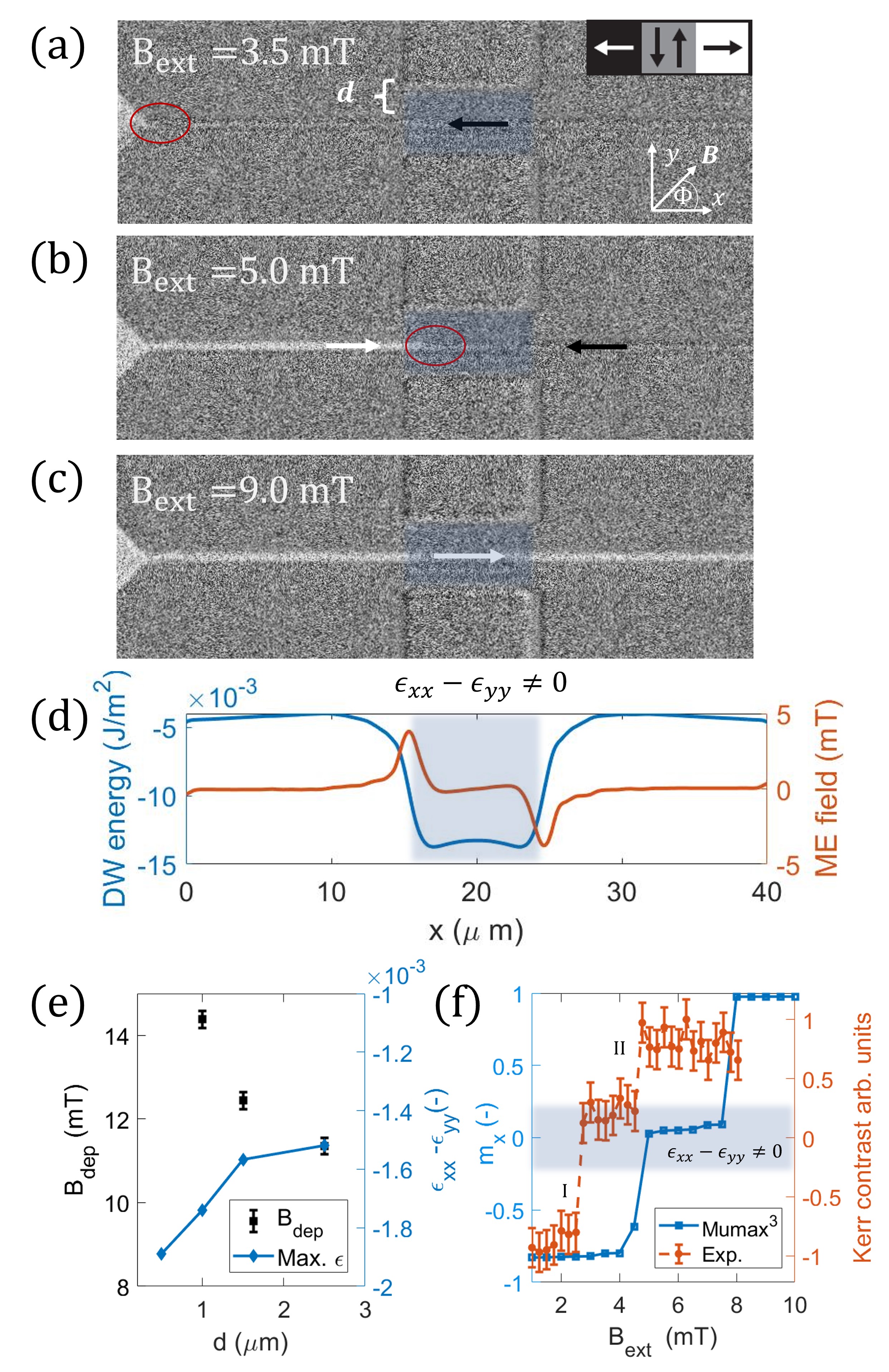
For this study, a 500 nm wide magnetic racetrack of Co70Fe30(30 nm) is considered together with a pair of square openings in the SiN 1010 µm2 in size. We use Kerr microscopy in transverse mode to image the magnetic state of the device, while in-plane magnetic field is applied parallel to the wire along . Figs. 3 (a)-(c) show the position of a DW along the magnetic racetrack as a function of the applied magnetic field. When the field is sufficiently large, the DW is injected from the reservoir (Fig. 3 (a)) into the magnetic wire. As can be seen in Fig. 3 (b), after injection the wall does not propagate until the end of the magnetic channel but is pinned in the area between the SiN openings corresponding to the strained area. The corresponding surface strain was shown with a simulation in Figs. 2 (a) and (c). Only for larger magnetic fields the wall can continue to propagate to the other end of the magnetic channel, as captured by Fig. 3 (c).
For a Ni81Fe19 sample with nearly no magnetostriction no DW pinning was found within the resolution of our measurement, supporting the idea of a strain-based pinning. We repeated the same measurement for devices with different distance between racetrack and openings. According to FEM simulations, the value of the (compressive) strain increases as the opening distance is reduced (blue diamonds in Fig. 3 (e)). As shown in Fig. 3 (e), the depinning field (black squares) increases from 11.0(2) mT to 14.5(2) mT for a distance between the opening and the magnetic racetrack decreasing from 2.5 to 1 µm. A larger depinning field for smaller opening spacing confirms that the magnetoelastic energy is indeed the dominant pinning cause in our systemLei et al. (2013); Franken et al. (2013).
To support our experimental findings, we performed micromagnetic simulations and 1D model calculations where the strain profile from FEM simulations was used. The results are summarized in Figs. 3 (d) and (f) and consider nanowires made of 30 nm thick Co40Fe40B20. For more details about the micromagnetic simulations and the 1D analytical model, see section S2 of the supplementary information. Fig. 3 (d) shows the DW energy per unit area and the corresponding magnetoelastic field as a function of the DW position for a nanowire nm wide, calculated considering the strain profile shown in Fig. 2 (a) and a rigid profile for the DW. Comparing Fig. 3 (d) with Fig. 3 (b), it is clear that the point where the DW sits is the minimum of DW energy. At the sides of the pinning site, the effective magnetoelastic field - proportional to according to Eq. 2 - is non-zero, and opposite to the applied external field. This equivalent force prevents the DW to move forward unless the external applied field is increased.
For the MumaxVansteenkiste et al. (2014) micromagnetic simulations a wire of 800 nm width has been considered. The magnetization has been initialized in the system with a DW on the left side of the strained area and then a magnetic field has been applied. Multiple dynamic simulations have been performed at different values of external magnetic field, and the results are summarized in Fig. 3 (f). As can be seen, the averaged magnetization along the direction (proportional to the DW position) coincides with the strained area (state I) for external fields . When the applied magnetic field is increased above , the domain wall is free to propagate and reaches the right end of the wire (state II). For comparison, the experimental values for the DW position as a function of is reported in Fig. 4 (f) for a 800 nm width Co40Fe40B20 wire. The pinning position (where ) coincides and discrepancies between the simulations and experiments for the value of can be due to thermally activated depinning events that are not fully captured by micromagnetic simulations.
The ability to adjust the maximum value of the strain, and thus the value of the depinning field, by changing the aperture design - as shown in Fig. 3 (e) - allows for the realization of a non-volatile magnetic field sensor capable of detecting discrete values of magnetic fields or current peaks from wires or coils in the sensor proximity. Previous work Al Bahri et al. (2019), suggested similar concepts, however, the one proposed here does not require sub 100 nm lithography resolution for the notches.
The conceptualization of the peak-field sensor is presented in Fig. 4. The device comprises of a magnetic nanowire for DWs propagation with a number of pinning sites along it. As shown in Figs. 4 (a) and (b) if the spacing between the SiN openings - acting as pinning sites - decreases, the strain magnitude is increased progressively. According to Fig. 3 (e), the depinning field will increase going from left to right. The device considered here presents four pair of openings and is therefore able to identify four discrete levels of external magnetic fields.
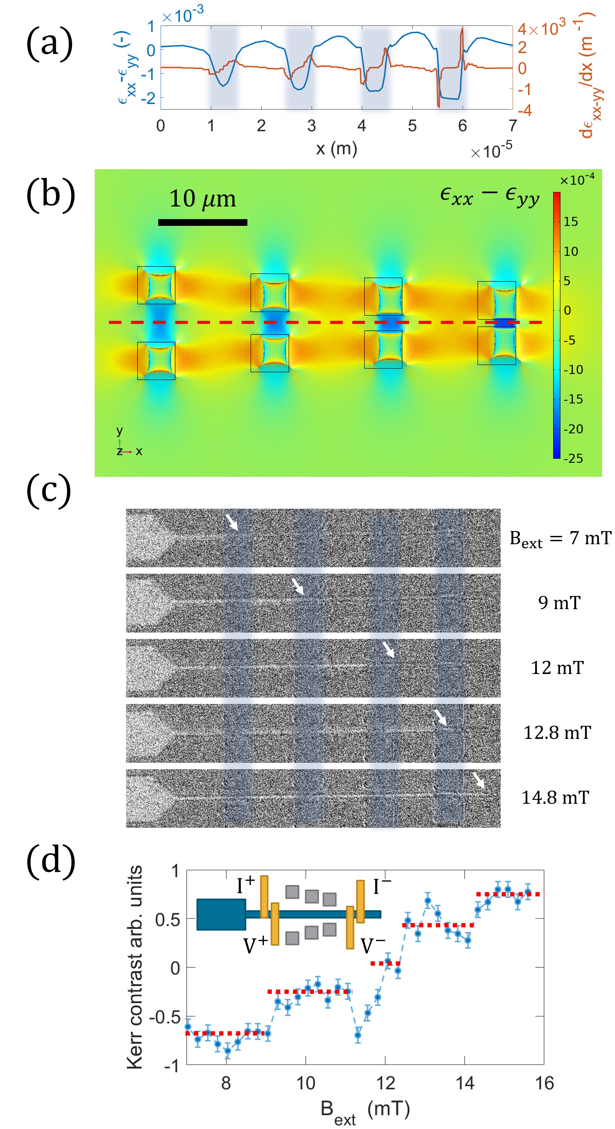
The proof of concept of the realized device is presented in Figs. 4 (c) and (d). We consider, in this case, a magnetic wire of 500 nm width and realized with a Co70Fe30 magnetic layer. The shape of the openings is 55 µm2 and the distance between the pairs is, in order 5, 3, 2 and 1 µm, as shown in Fig. 4 (b).
The device is initialized with large, negative magnetic field in the direction creating a uniform magnetic state. After that, positive magnetic filed is gradually increased while the magnetic state in the wire is monitored using Kerr microscopy. The magnetic contrast in Fig. 4 (d) shows how the magnetization has well defined discrete levels as is increased. This occurs because a DW propagating into the nanowire occupies only discrete positions along , as shown in Fig. 4 (c) in the strained area between the openings. The position of the DW in the magnetic channel (output) will indicate the maximum field (input) that the device has seen after initialization. The magnetic state has been measured in Fig. 4 (d) with optical methods, however, electrical readout of the DW position is possible using, e.g., Giant Magnetoresistive effect (GMR)Diegel et al. (2009) and two electrical contacts at the extremity of the magnetic channel. This sensing solution is particularly suitable for hardly accessible measurement environments and energy efficient devices as electrical power is required only for readout and initialization.
In summary, in this work we propose an validate a method for generating a local strain on a rigid substrate that is compatible with standard CMOS technologies. The intrinsic stress that occurs at the substrate/layer interface during SiN deposition can be modified when selected regions of the passivation layer are removed by etching. The strain is only modified near the removed material, as shown by FEM simulations. Using in-situ measurements of the magnetoelastic anisotropy, we experimentally determine the magnitude of the uniaxial strain up to . The magnitude and the gradient of the in-plane strain can be tuned depending on the geometry and position of the openings in the stress-generating layer. We validate the use of the above-mentioned strain gradients for the manipulation of magnetic domain walls in spintronic devices by exploiting magnetoelastic coupling in magnetostrictive materials. Using Kerr microscopy, we experimentally show how the magnetoelastic energy landscape enables the creation of engineered pinning sites which represent local energy minima for in-plane vortex walls. We report substantial pinning fields of up to 15 mT and support our experimental findings with micromagnetic simulations and 1D model calculations using a realistic strain profile. This provides the opportunity to realize an alternative generation of DW-based devices with technology compatible with wafer-level production, and an example of a discrete magnetic field or current sensor using imprinted strain gradients is demonstrated.
Supplementary Material
See supplementary material for details about the material parameters used, the finite-element-method and micromagnetic simulations and the anisotropy measurements.
Acknowledgements.
This project has received funding from the European Union’s Horizon 2020 research and innovation program under the Marie Skłodowska-Curie Grant Agreement No 860060 “Magnetism and the effect of Electric Field” (MagnEFi), the Deutsche Forschungsgemeinschaft (DFG, German Research Foundation) - TRR 173 - 268565370 (project A01 and B02), the DFG funded collaborative research center (CRC)1261 / project A10 and the Austrian Research Promotion Agency (FFG). The authors acknowledge support by the chip production facilities of Sensitec GmbH (Mainz, DE), where part of this work was carried out and the Max-Planck Graduate Centre with Johannes Gutenberg University.Author Declarations
Conflict of interest
The authors have no conflicts to disclose.
Data Sharing Policy
The data that support the findings of this study are available from the corresponding author upon reasonable request.
References
- Manipatruni, Nikonov, and Young (2018) S. Manipatruni, D. E. Nikonov, and I. A. Young, “Beyond CMOS computing with spin and polarization,” Nature Physics 14, 338–343 (2018).
- Ono et al. (1999) T. Ono, H. Miyajima, K. Shigeto, K. Mibu, N. Hosoito, and T. Shinjo, “Propagation of a magnetic domain wall in a submicrometer magnetic wire,” Science 284, 468–470 (1999).
- Atkinson et al. (2003) D. Atkinson, D. A. Allwood, G. Xiong, M. D. Cooke, C. C. Faulkner, and R. P. Cowburn, “Magnetic domain-wall dynamics in a submicrometre ferromagnetic structure,” Nature materials 2, 85–87 (2003).
- Hayashi et al. (2008) M. Hayashi, L. Thomas, R. Moriya, C. Rettner, and S. S. Parkin, “Current-controlled magnetic domain-wall nanowire shift register,” Science 320, 209–211 (2008).
- Kumar et al. (2022) D. Kumar, T. Jin, R. Sbiaa, M. Kläui, S. Bedanta, S. Fukami, D. Ravelosona, S.-H. Yang, X. Liu, and S. Piramanayagam, “Domain wall memory: Physics, materials, and devices,” Physics Reports 958, 1–35 (2022).
- Franken, Swagten, and Koopmans (2012) J. Franken, H. Swagten, and B. Koopmans, “Shift registers based on magnetic domain wall ratchets with perpendicular anisotropy,” Nature nanotechnology 7, 499–503 (2012).
- Luo et al. (2020) Z. Luo, A. Hrabec, T. P. Dao, G. Sala, S. Finizio, J. Feng, S. Mayr, J. Raabe, P. Gambardella, and L. J. Heyderman, “Current-driven magnetic domain-wall logic,” Nature 579, 214–218 (2020).
- Zhang et al. (2018) X. Zhang, N. Vernier, Z. Cao, Q. Leng, A. Cao, D. Ravelosona, and W. Zhao, “Magnetoresistive sensors based on the elasticity of domain walls,” Nanotechnology 29, 365502 (2018).
- Diegel et al. (2009) M. Diegel, S. Glathe, R. Mattheis, M. Scherzinger, and E. Halder, “A new four bit magnetic domain wall based multiturn counter,” IEEE Transactions on Magnetics 45, 3792–3795 (2009).
- Khan et al. (2021) M. A. Khan, J. Sun, B. Li, A. Przybysz, and J. Kosel, “Magnetic sensors-a review and recent technologies,” Engineering Research Express 3, 022005 (2021).
- Borie et al. (2017) B. Borie, J. Wahrhusen, H. Grimm, and M. Kläui, “Geometrically enhanced closed-loop multi-turn sensor devices that enable reliable magnetic domain wall motion,” Applied Physics Letters 111, 242402 (2017).
- Alamdar et al. (2021) M. Alamdar, T. Leonard, C. Cui, B. P. Rimal, L. Xue, O. G. Akinola, T. Patrick Xiao, J. S. Friedman, C. H. Bennett, M. J. Marinella, et al., “Domain wall-magnetic tunnel junction spin–orbit torque devices and circuits for in-memory computing,” Applied Physics Letters 118, 112401 (2021).
- Yue et al. (2019) K. Yue, Y. Liu, R. K. Lake, and A. C. Parker, “A brain-plausible neuromorphic on-the-fly learning system implemented with magnetic domain wall analog memristors,” Science advances 5, eaau8170 (2019).
- Boulle, Malinowski, and Kläui (2011) O. Boulle, G. Malinowski, and M. Kläui, “Current-induced domain wall motion in nanoscale ferromagnetic elements,” Materials Science and Engineering: R: Reports 72, 159–187 (2011).
- Omari et al. (2019) K. A. Omari, T. J. Broomhall, R. W. Dawidek, D. A. Allwood, R. C. Bradley, J. M. Wood, P. W. Fry, M. C. Rosamond, E. H. Linfield, M.-Y. Im, et al., “Toward chirality-encoded domain wall logic,” Advanced Functional Materials 29, 1807282 (2019).
- Shiu et al. (2021) D.-S. Shiu, K.-F. Lai, Y.-Y. Liu, Y.-T. Li, Z.-E. Gao, Y.-M. Kao, J.-C. Wu, and L. Horng, “Depinning behavior of the vortex domain wall at the asymmetric triangular notch in permalloy wires,” Journal of Physics Communications 5, 075014 (2021).
- Al Bahri et al. (2019) M. Al Bahri, B. Borie, T. Jin, R. Sbiaa, M. Kläui, and S. Piramanayagam, “Staggered magnetic nanowire devices for effective domain-wall pinning in racetrack memory,” Physical Review Applied 11, 024023 (2019).
- Fattouhi et al. (2022) M. Fattouhi, F. Garcia-Sanchez, R. Yanes, V. Raposo, E. Martinez, and L. Lopez-Diaz, “Absence of Walker breakdown in the dynamics of chiral Neel domain walls driven by in-plane strain gradients,” Physical Review Applied 18, 044023 (2022).
- Masciocchi et al. (2021) G. Masciocchi, M. Fattouhi, A. Kehlberger, L. Lopez-Diaz, M.-A. Syskaki, and M. Kläui, “Strain-controlled domain wall injection into nanowires for sensor applications,” Journal of Applied Physics 130, 183903 (2021).
- Lei et al. (2013) N. Lei, T. Devolder, G. Agnus, P. Aubert, L. Daniel, J.-V. Kim, W. Zhao, T. Trypiniotis, R. P. Cowburn, C. Chappert, et al., “Strain-controlled magnetic domain wall propagation in hybrid piezoelectric/ferromagnetic structures,” Nature communications 4, 1–7 (2013).
- Zhou et al. (2020) H. Zhou, S. Shi, D. Nian, S. Cui, J. Luo, Y. Qiu, H. Yang, M. Zhu, and G. Yu, “Voltage control of magnetic domain wall injection into strain-mediated multiferroic heterostructures,” Nanoscale 12, 14479–14486 (2020).
- Hu et al. (2016) J.-M. Hu, T. Yang, K. Momeni, X. Cheng, L. Chen, S. Lei, S. Zhang, S. Trolier-McKinstry, V. Gopalan, G. P. Carman, et al., “Fast magnetic domain-wall motion in a ring-shaped nanowire driven by a voltage,” Nano letters 16, 2341–2348 (2016).
- Dean et al. (2011) J. Dean, M. Bryan, T. Schrefl, and D. Allwood, “Stress-based control of magnetic nanowire domain walls in artificial multiferroic systems,” Journal of Applied Physics 109, 023915 (2011).
- Barra et al. (2021) A. Barra, A. Ross, O. Gomonay, L. Baldrati, A. Chavez, R. Lebrun, J. Schneider, P. Shirazi, Q. Wang, J. Sinova, et al., “Effective strain manipulation of the antiferromagnetic state of polycrystalline NiO,” Applied Physics Letters 118, 172408 (2021).
- Chu et al. (2009) M. Chu, Y. Sun, U. Aghoram, and S. E. Thompson, “Strain: A solution for higher carrier mobility in nanoscale MOSFETs,” Annual Review of Materials Research 39, 203–229 (2009).
- Doherty et al. (2020) J. L. Doherty, S. G. Noyce, Z. Cheng, H. Abuzaid, and A. D. Franklin, “Capping layers to improve the electrical stress stability of MoS2 transistors,” ACS applied materials & interfaces 12, 35698–35706 (2020).
- Martin et al. (2009) N. Martin, J. McCord, A. Gerber, T. Strache, T. Gemming, I. Mönch, N. Farag, R. Schäfer, J. Fassbender, E. Quandt, et al., “Local stress engineering of magnetic anisotropy in soft magnetic thin films,” Applied Physics Letters 94, 062506 (2009).
- McCord (2015) J. McCord, “Progress in magnetic domain observation by advanced magneto-optical microscopy,” Journal of Physics D: Applied Physics 48, 333001 (2015).
- Soldatov and Schäfer (2017) I. Soldatov and R. Schäfer, “Selective sensitivity in Kerr microscopy,” Review of Scientific Instruments 88, 073701 (2017).
- Ohring (1992) M. Ohring, “The materials science of thin films,” Appl. Opt 31, 7162 (1992).
- Marks, Hassan, and Cheong (2014) M. R. Marks, Z. Hassan, and K. Y. Cheong, “Characterization methods for ultrathin wafer and die quality: A review,” IEEE Transactions on components, packaging and manufacturing technology 4, 2042–2057 (2014).
- COMSOL AB, Stockholm, Sweden (2023) COMSOL AB, Stockholm, Sweden, “Comsol multiphysics® v. 6.1,” (2023).
- Finizio et al. (2014) S. Finizio, M. Foerster, M. Buzzi, B. Krüger, M. Jourdan, C. A. Vaz, J. Hockel, T. Miyawaki, A. Tkach, S. Valencia, et al., “Magnetic anisotropy engineering in thin film Ni nanostructures by magnetoelastic coupling,” Physical Review Applied 1, 021001 (2014).
- Masciocchi et al. (2022) G. Masciocchi, J. W. van der Jagt, M.-A. Syskaki, A. Lamperti, N. Wolff, A. Lotnyk, J. Langer, L. Kienle, G. Jakob, B. Borie, et al., “Control of magnetoelastic coupling in Ni/Fe multilayers using He+ ion irradiation,” Applied Physics Letters 121, 182401 (2022).
- McCord (2004) J. McCord, “Irregular domain patterns in structured magnetic thick films,” Journal of applied physics 95, 6855–6857 (2004).
- Urs et al. (2014) N. O. Urs, I. Teliban, A. Piorra, R. Knöchel, E. Quandt, and J. McCord, “Origin of hysteretic magnetoelastic behavior in magnetoelectric 2-2 composites,” Applied Physics Letters 105, 202406 (2014).
- Thórarinsdóttir et al. (2022) K. Thórarinsdóttir, N. Strandqvist, V. Sigurjónsdóttir, E. Thorsteinsson, B. Hjörvarsson, and F. Magnus, “Finding order in disorder: Magnetic coupling distributions and competing anisotropies in an amorphous metal alloy,” APL Materials 10, 041103 (2022).
- Wen et al. (2020) D. Wen, Z. Chen, W. Li, M. Qin, D. Chen, Z. Fan, M. Zeng, X. Lu, X. Gao, and J.-M. Liu, “Ultralow-loss domain wall motion driven by a magnetocrystalline anisotropy gradient in an antiferromagnetic nanowire,” Physical Review Research 2, 013166 (2020).
- Fattouhi et al. (2021) M. Fattouhi, F. García-Sánchez, R. Yanes, V. Raposo, E. Martínez, and L. Lopez-Diaz, “Electric Field Control of the Skyrmion Hall Effect in Piezoelectric-Magnetic Devices,” Physical Review Applied 16, 044035 (2021).
- Franken et al. (2013) J. Franken, Y. Yin, A. Schellekens, A. van den Brink, H. Swagten, and B. Koopmans, “Voltage-gated pinning in a magnetic domain-wall conduit,” Applied Physics Letters 103, 102411 (2013).
- Vansteenkiste et al. (2014) A. Vansteenkiste, J. Leliaert, M. Dvornik, M. Helsen, F. Garcia-Sanchez, and B. Van Waeyenberge, “The design and verification of mumax3,” AIP advances 4, 107133 (2014).