/csteps/inner color=white \pgfkeys/csteps/outer color=black \pgfkeys/csteps/fill color=black \pgfkeys/csteps/inner xsep=1pt \pgfkeys/csteps/inner ysep=1pt
Cheshire: A Lightweight, Linux-Capable
RISC-V Host Platform for Domain-Specific Accelerator Plug-In
Abstract
Power and cost constraints in the internet-of-things (IoT) extreme-edge and TinyML domains, coupled with increasing performance requirements, motivate a trend toward heterogeneous architectures. These designs use energy-efficient application-class host processors to coordinate compute-specialized multicore accelerators, amortizing the architectural costs of operating system support and external communication. This brief presents Cheshire, a lightweight and modular 64-bit Linux-capable host platform designed for the seamless plug-in of domain-specific accelerators. It features a unique low-pin-count DRAM interface, a last-level cache configurable as scratchpad memory, and a DMA engine enabling efficient data movement to or from accelerators or DRAM. It also provides numerous optional IO peripherals including UART, SPI, I2C, VGA, and GPIOs. Cheshire’s synthesizable RTL description, comprising all of its peripherals and its fully digital DRAM interface, is available free and open-source. We implemented and fabricated Cheshire as a silicon demonstrator called Neo in TSMC’s 65nm CMOS technology. At 1.2 V, Neo achieves clock frequencies of up to 325 MHz while not exceeding 300 mW in total power on data-intensive computational workloads. Its RPC DRAM interface consumes only 250 pJ/B and incurs only 3.5 kGE in area for its PHY while attaining a peak transfer rate of 750 MB/s at 200 MHz.
Index Terms:
RISC-V, Linux, PHYs, memory controllers, domain-specific architectures, heterogeneous computing, VLSII Introduction
With Koomey’s law111Observed from the 1940s to early 2000s, Koomey’s Law states that the energy efficiency of computers doubles every 1.57 years. [1] slowing down, computer architects turn to hardware specialization to meet the rising energy efficiency requirements of data-intensive applications like machine learning (ML) and near-sensor processing. Today’s heterogeneous architectures couple conventional application-class (AC) host processors to domain-specific architectures (DSAs) or programmable many-core accelerators (PMCAs) [2, 3, 4, 5], improving energy efficiency while maintaining high programmability and general-purpose operating system (GPOS) support. Thus, to maximize compute efficiency in heterogeneous systems, architects should maximize the area and energy resources spent on efficient accelerators and minimize the cost and energy footprint of AC hosts.
Heterogeneous architectures are established in mobile and high-performance applications: silicon-proven industrial [6, 7, 8] and academic [9, 10] systems-on-chip (SoCs) typically target large power envelopes or multiple AC cores. However, heterogeneity is now penetrating the internet of things (IoT) extreme-edge and TinyML domains where power and cost constraints are extremely tight. Heterogeneous SoCs in these domains [11, 12] typically use lightweight 32-bit microcontrollers without AC capabilities or GPOS support as management processors. The recent HULK-V [13] SoC demonstrates a more capable host by coupling a Linux-capable 64-bit RISC-V manager core to an eight-core PMCA for high-end tinyML applications. However, it has not been silicon-proven, and its PMCA’s ad-hoc integration does not provide a reusable interface. Furthermore, HULK-V’s external HyperRAM [14] memory interface is low-bandwidth, limiting scalability and potentially incurring host-accelerator memory bottlenecks.
To address these shortcomings, we present Cheshire, an energy-efficient, Linux-capable, 64-bit RISC-V host platform for the seamless heterogeneous plug-in of DSAs such as [15, 16]. Cheshire is fully modular and provides a configurable interconnect, numerous optional peripherals, and a direct memory access (DMA) engine to decouple host-DSA communication. It integrates the first synthesizable open-source interface for reduced pin count (RPC) DRAM, a recent low-pin-count DRAM solution incurring lower integration cost and effort than low-power double data rate (LPDDR) DRAM, but significantly higher bandwidth than HyperRAM at comparable energy efficiency. Cheshire’s synthesizable register-transfer level (RTL) description and FPGA implementation are available open-source222https://github.com/pulp-platform/cheshire for Cheshire and https://github.com/pulp-platform/rpc_dram_controller for its RPC DRAM interface.. We present the following contributions:
-
•
A minimal, customizable, and energy-efficient Linux-capable RV64GC host platform that can easily be co-integrated with on-chip or chiplet DSAs; we provide a configurable Advanced eXtensible Interface 4 (AXI4) interconnect and a digital die-to-die (D2D) interface.
-
•
The first fully digital, technology-independent RPC-DRAM-compliant memory interface, which incurs only 22 switching IOs and in PHY area. It enables memory accesses at only while attaining a peak transfer rate of at , outperforming existing HyperRAM solutions. To the best of our knowledge, this is the first characterization of reduced-pin-count DRAM (RPC DRAM) in a taped-out open-source SoC.
-
•
An agile memory system, enabling accesses to external RPC DRAM in only 8 cycles for a transfer while interacting with DSA memory space only when desired.
-
•
A standalone demonstrator chip called Neo, fabricated in TSMC’s node. At , Neo achieves clock frequencies of up to while consuming less than during data-intensive computational workloads.
II Architecture
In the following section, we present the overall architecture of Cheshire, followed by an in-depth discussion of the fully-digital, technology-agnostic RPC DRAM interface.
II-A Cheshire Platform
Cheshire is based on the energy-efficient 64-bit CVA6 [17] AC processor. It includes all hardware necessary to boot and run a GPOS like Linux autonomously, such as RISC-V-compliant core-local and platform interrupt controllers, various optional standard IO interfaces to access external storage and peripherals, and a DRAM interface. Off-chip DRAM is essential as the - memory footprint of simple embedded Linux systems [18] usually does not fit into on-chip memory.
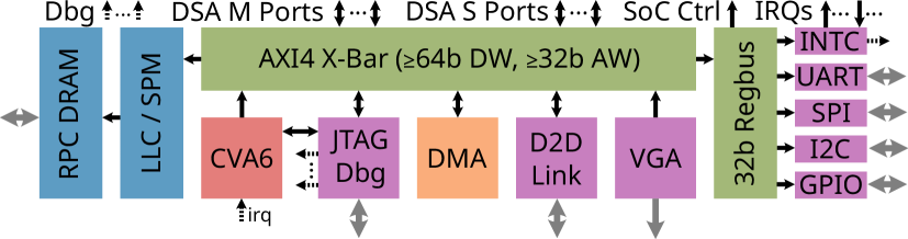
Figure 1 shows Cheshire’s architecture. A crossbar [19] using Arm’s widespread AXI4 protocol[20] connects the CVA6 processor to RPC DRAM, the DSA, and other Cheshire-internal components. The crossbar’s address width, data width, and the number of AXI4 DSA manager and subordinate ports are configurable to suit the target system’s bandwidth and addressing needs. Simpler subordinates without burst or out-of-order transaction support are attached through a lightweight, extensible Regbus[21] demultiplexer, minimizing the crossbar’s area and energy footprint.
Cheshire’s RPC DRAM is connected through a configurable last-level cache (LLC). Each of the LLC’s ways may individually be configured to serve as a scratchpad memory (SPM) at runtime, providing the host with fast internal static random access memory (SRAM) when needed. A RISC-V compliant debug module, backed by a JTAG transport module, enables live external debugging of CVA6 and any configured number of external RISC-V harts, e.g., those in PMCA DSAs. Likewise, the interrupt controllers support a configurable number of external sources and targets.
Cheshire provides various optional peripherals, including a flexible AXI4 DMA engine[22] for efficient data movement, a VGA controller for display output, and a digital D2D link for communication with off-chip systems. It also provides a UART for serial communication, a GPIO module, and I2C and SPI hosts to access external peripherals. All peripherals seamlessly integrate through AXI4 or Regbus interfaces and provide well-established feature sets for full compatibility with existing Linux drivers. An additional SoC control port connects to Cheshire-external on-chip devices essential for operation, such as clock generators, IO multiplexers, or clock and power domain controllers.
Cheshire has a built-in boot ROM, allowing for passive preloading through JTAG, UART, or the D2D link or autonomous boot from an external SPI Flash, I2C EEPROM, or SD card with Globally Unique Identifier Partition Table (GPT) support. If configured, it invokes an external ROM first to set up the surrounding chip through the SoC control port. Compiled with -Os flags and full-program link-time optimization, Cheshire’s boot ROM is in size.
Although we use a single CVA6 as Cheshire’s AC processor, multiple coherent CVA6 cores or another AC processor could be integrated instead; here, we focus on a minimal AC host.
We provide an open-source FPGA implementation of Cheshire, currently targeting Digilent’s Genesys II board, which enables the rapid prototyping and characterization of heterogeneous systems.
II-B RPC DRAM Interface
II-B1 Background
RPC DRAM is specified to use a minimum number of signals to deliver DDR 3-level in-system bandwidth [23]. Its defining feature is its interface, which multiplexes data, addresses, and commands onto a common data bus (DB) to minimize the needed pins. Command/address (CA) control can be sent concurrently with data by using a single multi-function pin to transmit serial commands, offering the high transaction efficiency of DDR 3 at the cost of just 22 switching signals for a 16-bit wide DB. The strobe pins DQS and DQS# sample DB with a preamble identical to DDR 3.
Alternative DRAM solutions with low-pin-count interfaces have been proposed. Cypress’ HyperRAM [14] requires only 12 switching IOs for an 8-bit shared bus. However, transfer rates are limited to at or less, and its self-refresh precludes advanced controller-side scheduling. Antmicro proposes an FPGA-based Rowhammer testing platform based on the LiteDRAM memory controller [24]. The controller supports several DDR memory types and recently added an RPC physical interface circuit (PHY) implementation. Although open-source, this PHY targets FPGAs only.
II-B2 Interface
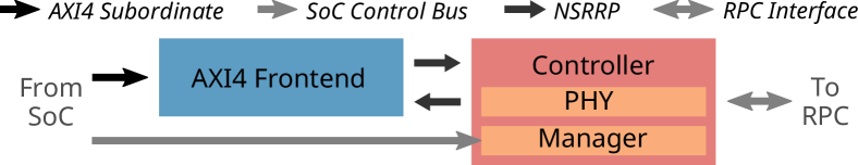
Figure 2 depicts our RPC DRAM interface. It is comprised of two parts: a controller implementing the off-chip RPC protocol [23] and an AXI4 frontend implementing an AXI4-compliant subordinate. To enable easy adaptation to on-chip protocols other than AXI4, the controller and frontend are connected through a generic interface we call non-stallable request-response protocol (NSRRP); its datawidth is or one word in the RPC DRAM standard. In the following, we will discuss the controller and AXI4 frontend in detail.
II-B3 Controller
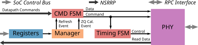
Figure 3 depicts the internal controller architecture. As shown, the controller receives datapath commands from the frontend. These generic commands are passed to the command FSM, which decomposes them into RPC DRAM-specific commands. For example, a generic datapath read is decomposed into 1) an activate of the corresponding bank and row, 2) a read of consecutive RPC DRAM words, and 3) a precharge to close the bank and prepare it for the next access.
In addition to datapath commands issued by the frontend, the command FSM also handles management commands issued by a manager module inside the controller. The manager has three responsibilities: 1) it initializes the RPC DRAM device on startup, 2) it periodically refreshes active banks, and 3) it performs ZQ calibration when necessary. For these tasks, the manager uses configurable timing parameters, which can be set through a memory-mapped register file.
The command FSM passes its generated RPC DRAM commands to the timing FSM, which performs two tasks: 1) it times commands, ensuring that they adhere to protocol constraints like cycle alignment and minimum delays, and 2) it times the physical interface, which includes controlling the chip select signals, gating the output strobe, and multiplexing data, mask, and commands onto the DB.
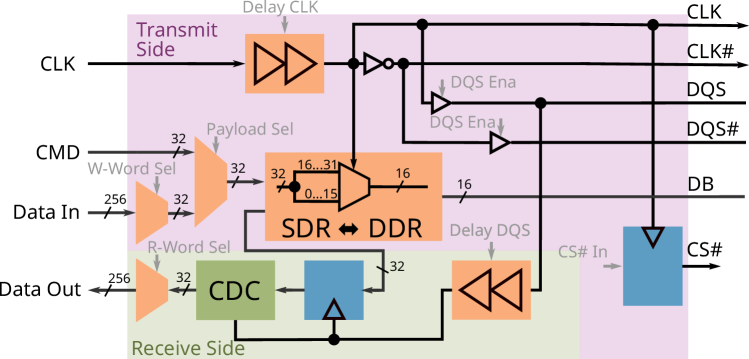
The physical interface circuit (PHY), shown in Figure 4, implements a low-power, digital-only, technology-agnostic RPC DRAM physical layer without internal clock generation. As shown, the PHY is composed of two parts: the transmit side sends data to the RPC DRAM, and the receive side accepts data from the RPC DRAM.
The transmit side creates 90- and 270-degree phase-shifted clocks with a configurable delay line to drive the strobe signals DQS and DQS#, which are selectively enabled by the timing FSM. Any data words to be sent to the RPC DRAM are first serialized to subwords; the timing FSM then arbitrates between sending commands and data subwords using a multiplexer. The chosen payload is converted from single data rate (SDR) to DDR using clock-driven multiplexers as shown and placed on the DB.
The receive side accepts the strobe signal DQS in phase with the data read from the RPC DRAM chip through the DB pins. The received data is converted to SDR, then sampled by a delayed strobe generated with another configurable delay line. After passing through a clock domain crossing, the read data is packed to form complete words and then sent back to the AXI4 frontend over an NSRRP channel.
II-B4 AXI4 Frontend
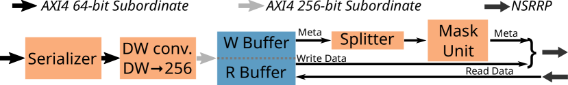
The frontend, shown in Figure 5, implements an AXI4-compliant subordinate. Incoming requests are first serialized as the RPC DRAM controller operates strictly in order. In the current design, transfers from different AXI4 IDs are handled first come, first serve; we plan to implement transfer prioritization using AXI4’s quality of service (QoS) signals in future versions. After serialization, a datawidth converter converts the RPC DRAM interfaces’ configured datawidth ( in the case of Neo) to RPC’s word size.
While AXI4 allows transfers to be stalled on any beat, RPC bursts cannot be stalled once launched. Hence, both reads and writes are buffered. Write data is buffered and released once the buffer contains all data needed for the next write. Read data is forwarded to the AXI4 bus as soon as possible to minimize latency and buffered only on AXI4 bus stalls.
The splitter splits NSRRP transactions at boundaries to comply with the RPC protocol. RPC DRAM implements unaligned transfers by introducing a first and a last mask. The masks are transmitted between the write command and the corresponding data. The mask unit derives these two masks from the strobe information included in AXI4 requests.
III Evaluation
We evaluate Cheshire through a silicon demonstrator named Neo, which was designed, implemented, and fabricated using TSMC’s node with nine metal layers. Neo was synthesized using Synopsys Design Compiler 2019.03 and implemented using Cadence Innovus 2019.10, targeting a system clock in the SS corner at and using low- cells. We will first describe how we configured Cheshire for Neo, then characterize the RPC DRAM and the AXI4 DSA interfaces in terms of functional performance (Section III-B) and silicon implementation performance (Section III-C).
III-A Silicon Demonstrator
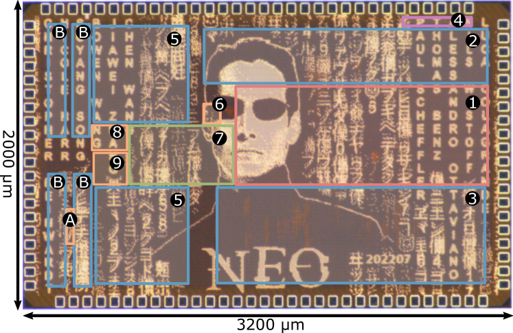
Figure 6 shows an annotated die shot of Neo. Its die is housed in a QFN64 package. We use a core voltage of and a global IO voltage of to comply with the RPC DRAM interface. We configure Cheshire without DSA ports as we do not integrate any accelerator in this demonstrator. Neo features of SPM, data, and addresses; its CVA6 core is configured with 8-way level-one data and instruction caches. The RPC DRAM frontend is configured with buffers for read and write each. We include an on-chip frequency-locked loop (FLL) for internal clock generation and control.
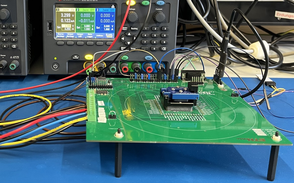
We test Neo on a custom-made bring-up PCB shown in Figure 7. This board can be connected to an industry-grade automated test equipment (ATE) device (Advantest SoCV93000) or operated standalone. In standalone mode, the board provides Neo with a reference clock to lock its internal FLL and a debounced reset; it also features a set of peripherals and connectors to boot and run applications, including a RPC DRAM chip (EM6GA16LBXA-12H) connected to Neo and used for testing and measurements. User interaction may happen through UART and VGA output.
III-B Functional Performance
Functional evaluation is performed through cycle-accurate RTL simulation. For all presented results, we leverage the efficient data movement capabilities of the DMA engine, which enables decoupled, high throughput host-DSA transfers and frees CVA6 from handling data movement tasks.
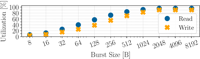
RPC DRAM specifies a maximum bus clock frequency of , outperforming competing solutions. Provided Neo’s DB bus and an operating frequency of with DDR signaling, the peak attainable throughput is = , where is the relative bus utilization. Figure 8 shows the attained RPC bus utilization for both the read and write datapaths. The DMA is programmed to issue write and read transfers at increasing burst sizes starting from . The interface bus utilization plateaus close to peak utilization () for bursts in size or larger as they are decomposed into smaller transfers by the AXI4 frontend’s transfer splitter. While the RPC pre- and postamble incur a constant, protocol-defined overhead independent of transfer size and controller implementation, bus utilization on reads is on average 1.3 higher than on corresponding writes; this is because read data is passed to the AXI4 bus as soon as possible whereas writes are deferred until enough data is buffered.
RPC DRAM proves its superiority in attainable bandwidth and area footprint against one of its closest competitors, HyperBus, which was implemented in several academic works [12, 13]. HyperRAM occupies more PCB area, has a much lower maximum data rate of , and is limited to a maximum frequency of only [14], restricting its applicability in high-bandwidth energy-efficient scenarios.
III-C Silicon performance
III-C1 Area breakdown
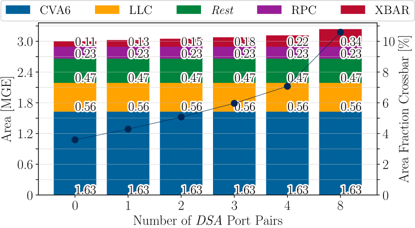
Figure 6 shows Neo’s die, highlighting the approximate location and size of its main components. Figure 9 reports Cheshire’s exact area breakdown in , progressively increasing the number of DSA manager-subordinate port pairs attached to its main AXI4 crossbar. The leftmost bar corresponds to Neo’s configuration without DSA ports. In all considered cases, CVA6 dominates Cheshire’s area, while the RPC DRAM controller accounts for at most . As we increase the number of DSA ports, the all-to-all AXI4 crossbar grows from to of Cheshire, increasing its area by at most for eight port pairs compared to Neo’s configuration without DSA ports. While crossbar scaling is a limiting factor for large numbers of port pairs, DSAs with many managers or subordinates can use a sub-interconnect, larger data widths, or sparse connectivity to facilitate scaling.
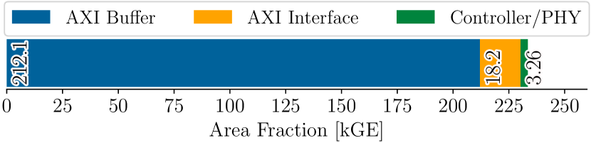
Figure 10 shows the area breakdown of Neo’s RPC DRAM controller. The manager module, command/timing FSM, and digital PHY occupy only or of the controller’s area, confirming the extremely low area overhead incurred by the RPC protocol for its memory interface. Most of the controller’s area overhead is due to the buffers holding AXI4 beats. In Neo, these buffers are over-provisioned to simplify the initial design of the AXI4 frontend, but their size can be further reduced in future versions. Despite this, our controller occupies only of the area and of the beachfront of an existing full-pin-count DDR 3 controller [25].
III-C2 Energy efficiency
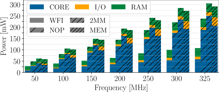
Figure 11 shows Neo’s power consumption for different scenarios and frequencies as measured on the bring-up board; each scenario explores an operational corner with different computational and memory intensities. We focus here on evaluating the Cheshire platform; for further benchmarks of the CVA6 processor, we refer the reader to its publication [17]. The bring-up board provides three power domains with their supplies: core, io, and ram. core feeds Neo’s core area logic and SRAMs, io provides power to its pads, and ram supplies the RPC DRAM memory chips.
In the WFI scenario, CVA6 is waiting for an interrupt, idling without fetching or decoding instructions; this provides a power baseline with minimal switching. In NOP, CVA6 loops on a body of nops, establishing a floor for actively fetching, branching, and decoding workloads with few stalls. 2MM runs an optimized double-precision floating-point matrix multiplication with arguments and results in RPC DRAM, keeping reusable matrix tiles in SPM. MEM writes high-throughput bursts to RPC DRAM using the DMA engine.
At a core supply of , Neo achieves clock frequencies of up to and remains within a power envelope even in data-intensive computational scenarios like 2MM. All power contributions scale linearly with frequency as expected, and core power dominates in almost all cases; at , of MEM power is consumed in core. Since the version of RPC DRAM interface proposed in this manuscript does not make use of the technology’s Deep Power Down state, all benchmarks show an ram idle power consumption. That being said, the RPC DRAM interface’s io power at for MEM is lower than that of an existing DDR 3 interface under high load [25].
We use MEM to compute RPC DRAM’s transfer efficiency. We consider only the write direction, representing the worst-case scenario regarding buffering as discussed in Section II. Given the maximum bandwidth measured in Section III-B, RPC DRAM’s interface energy per transferred byte is . This result is comparable to reported energy-per-byte consumptions in recent works integrating lower-bandwidth memories like HyperRAM [12].
IV Conclusion
This work presents Cheshire, a lightweight, modular, and open-source 64-bit Linux-capable host platform designed to plug in DSAs seamlessly. Cheshire features a unique RPC DRAM interface, a last-level cache, configurable as scratchpad memory, and a DMA engine enabling efficient data movement to or from accelerators or DRAM. It also provides numerous optional peripherals, including UART, SPI, I2C, a GPIO module, and VGA for display output. We implement and fabricate Cheshire as a silicon demonstrator called Neo in TSMC’s 65nm CMOS technology. At , Neo achieves clock frequencies of up to while not exceeding in total power even in data-intensive computational scenarios. Its DRAM interface consumes only while incurring only in area for its PHY and attaining a peak transfer rate of at .
Acknowledgments
We thank the reviewers for their feedback. We thank C. Jinfan, V. Krishna, R. Zhou, N. Narr, C. Reinwardt, S. Song, B. Wang, C. Wang, J. Zhang, N. Wistoff, and L. Colagrande for their contributions to this research. We also thank Etron Technology Inc., in particular R. Crisp, for their support. This work is supported in part through the FRACTAL (877056) project, which received funding from the ECSEL Joint Undertaking (JU) and TRISTAN (101095947) project, which received funding from the HORIZON KDT-JU programme.
References
- [1] J. Koomey, S. Berard, M. Sanchez, and H. Wong, “Implications of historical trends in the electrical efficiency of computing,” IEEE Ann. Hist. Comput., vol. 33, no. 3, pp. 46–54, 2011.
- [2] Y. Chi, W. Qiao, A. Sohrabizadeh, J. Wang, and J. Cong, “Democratizing domain-specific computing,” Commun. ACM, vol. 66, no. 1, p. 74–85, dec 2022.
- [3] J. L. Hennessy and D. A. Patterson, “A new golden age for computer architecture,” Commun. ACM, vol. 62, no. 2, p. 48–60, jan 2019.
- [4] Y. Zhao, R. Xie, G. Xin, and J. Han, “A high-performance domain-specific processor with matrix extension of risc-v for module-lwe applications,” IEEE Trans. Circuits Syst. I: Reg. Papers, vol. 69, no. 7, pp. 2871–2884, 2022.
- [5] R. Paludo and L. Sousa, “Ntt architecture for a linux-ready risc-v fully-homomorphic encryption accelerator,” IEEE Trans. Circuits Syst. I: Reg. Papers, vol. 69, no. 7, pp. 2669–2682, 2022.
- [6] Raspberry Pi Foundation, “Rasperry pi zero,” https://www.raspberrypi.com/products/raspberry-pi-zero, 2020.
- [7] M. Ditty, “Nvidia orin system-on-chip,” in 2022 IEEE Hot Chips 34 Symp., 2022, pp. 1–17.
- [8] SiFive, “Hifive unmatched,” https://www.sifive.com/boards/hifive-unmatched, 2022.
- [9] J. Zuckerman, P. Mantovani, D. Giri, and L. P. Carloni, “Enabling heterogeneous, multicore soc research with risc-v and esp,” 2022.
- [10] J. Balkind, K. Lim, M. Schaffner, F. Gao, G. Chirkov, A. Li, A. Lavrov, T. M. Nguyen, Y. Fu, F. Zaruba, K. Gulati, L. Benini, and D. Wentzlaff, BYOC: A ”Bring Your Own Core” Framework for Heterogeneous-ISA Research. New York, NY, USA: ACM, 2020, p. 699–714.
- [11] A. Di Mauro, M. Scherer, D. Rossi, and L. Benini, “Kraken: A direct event/frame-based multi-sensor fusion soc for ultra-efficient visual processing in nano-uavs,” in IEEE Hot Chips 34 Symp., 2022, pp. 1–19.
- [12] D. Rossi, F. Conti, M. Eggiman, A. D. Mauro, G. Tagliavini, S. Mach, M. Guermandi, A. Pullini, I. Loi, J. Chen, E. Flamand, and L. Benini, “Vega: A ten-core SoC for IoT endnodes with DNN acceleration and cognitive wake-up from MRAM-based state-retentive sleep mode,” IEEE J. Solid-State Circuits, vol. 57, no. 1, pp. 127–139, jan 2022.
- [13] L. Valente, Y. Tortorella, M. Sinigaglia, G. Tagliavini, A. Capotondi, L. Benini, and D. Rossi, “HULK-V: a Heterogeneous Ultra-low-power Linux capable RISC-V SoC,” in 2023 Design, Automation & Test in Europe Conference & Exhibition (DATE), 2023.
- [14] Cypress, “Hyperram & octal xspi ram memory,” https://www.cypress.com/products/hyperram-octal-xspi-ram-memory.
- [15] A. Garofalo, M. Rusci, F. Conti, D. Rossi, and L. Benini, “Pulp-nn: A computing library for quantized neural network inference at the edge on risc-v based parallel ultra low power clusters,” in 26th IEEE Int. Conf. Electronics, Circuits and Syst., 2019, pp. 33–36.
- [16] E. Manor and S. Greenberg, “Custom hardware inference accelerator for tensorflow lite for microcontrollers,” IEEE Access, vol. 10, pp. 73 484–73 493, 2022.
- [17] F. Zaruba and L. Benini, “The cost of application-class processing: Energy and performance analysis of a linux-ready 1.7-ghz 64-bit risc-v core in 22-nm fdsoi technology,” IEEE Trans. Very Large Scale Integration (VLSI) Syst., vol. 27, no. 11, pp. 2629–2640, Nov 2019.
- [18] M. Opdenacker, “Linux in less than 4 mb of ram,” https://bootlin.com/pub/conferences/2017/jdll/opdenacker-embedded-linux-in-less-than-4mb-of-ram/, 2017.
- [19] A. Kurth, W. Ronninger, T. Benz, M. Cavalcante, F. Schuiki, F. Zaruba, and L. Benini, “An open-source platform for high-performance non-coherent on-chip communication,” IEEE Trans. Comput., pp. 1–1, 2021.
- [20] A. Limited, “Amba axi and ace protocol specification version h.c,” https://developer.arm.com/documentation/ihi0022/hc, 2021.
- [21] Generic Register Interface, PULP Platform Contributors. [Online]. Available: https://github.com/pulp-platform/register_interface
- [22] T. Benz, M. Rogenmoser, P. Scheffler, S. Riedel, A. Ottaviano, A. Kurth, T. Hoefler, and L. Benini, “A high-performance, energy-efficient modular dma engine architecture,” 2023.
- [23] Etron Technology, “256Mb high bandwidth rpc dram,” https://etronamerica.com/wp-content/uploads/2019/05/EM6GA16LGDABMACAEA-RPC-DRAM_Rev.-1.0.pdf, 2019.
- [24] Antmicro, “Open source ddr controller framework for mitigating rowhammer,” https://antmicro.com/blog/2021/08/open-source-ddr-test-framework-for-rowhammer/, 2021.
- [25] C. Sudarshan, J. Lappas, C. Weis, D. M. Mathew, M. Jung, and N. Wehn, “A lean, low power, low latency dram memory controller for transprecision computing,” in Embedded Comput. Syst.: Architectures, Model., Simul. Springer Int. Publishing, 2019, pp. 429–441.