Multi-module microwave assembly for fast read-out and charge noise characterization of silicon quantum dots
Abstract
Fast measurements of quantum devices is important in areas such as quantum sensing, quantum computing and nanodevice quality analysis. Here, we develop a superconductor-semiconductor multi-module microwave assembly to demonstrate charge state readout at the state-of-the-art. The assembly consist of a superconducting readout resonator interfaced to a silicon-on-insulator (SOI) chiplet containing quantum dots (QDs) in a high- nanowire transistor. The superconducting chiplet contains resonant and coupling elements as well as filters that, when interfaced with the silicon chip, result in a resonant frequency GHz, a loaded quality factor , and a resonator impedance . Combined with the large gate lever arms of SOI technology, we achieve a minimum integration time for single and double QD transitions of 2.77 ns and 13.5 ns, respectively. We utilize the assembly to measure charge noise over 9 decades of frequency up to 500 kHz and find a 1/ dependence across the whole frequency spectrum as well as a charge noise level of 4 eV/ at 1 Hz. The modular microwave circuitry presented here can be directly utilized in conjunction with other quantum device to improve the readout performance as well as enable large bandwidth noise spectroscopy, all without the complexity of superconductor-semiconductor monolithic fabrication.
I Introduction
Fast charge readout is a desired quality for many solid-state quantum technologies [1, 2, 3, 4, 5]. It enables dynamical studies of these systems [6, 7], provides a means to explore their noise spectrum [8] and for example, finds applications in qubit state readout [9, 10, 11], measurement of mechanical motion [12] and fast thermometry at the nanoscale [13, 14].
Particularly, for silicon-based spin qubits, fast charge measurements along with spin-to-charge conversion techniques [15, 16] have enabled high-fidelity read out in short timescales, fulfilling one of the requirements for fault-tolerant quantum computing [17]. In conjunction with high-fidelity one- and two-qubit gates [18, 19, 20], the demonstrations of simple instances of quantum error correction [21], the operation of a six-qubit processors [22] and the compatibility with advanced manufacturing techniques [23, 24, 25, 26, 27], these steps show important progress towards a scalable silicon-based quantum computer [28].
Silicon spin qubits are typically read using dissipative charge sensors like the single-electron transistor (SET) whose bandwidth can be increased to the MHz range by embedding the device in a high-frequency resonator [29]. To minimise the impact of the sensing method on quantum processor layout [30, 31, 32, 33], recent work has focused on resonant dispersive readout methods such as the single-electron box (SEB) [34, 35] and in-situ readout [36, 37]. Monolithic integration of the device and resonator on the same chip has lead to the highest charge readout rates both for the SEB [38] as well as for in-situ readout [39] due to the reduced parasitics that result in higher operation frequency, quality factor and resonator impedance. Additionally, monolithically integrated resonators have been used to explore circuit quantum electrodynamics with silicon spins [40, 41, 42]. However, monolithic integration poses important fabrication challenges and may interfere with high qubit connectivity. On the other hand, multi-module microwave assemblies, in which the resonant circuitry is fabricated in a separate chiplet to the device [43], offers the flexibility to independently optimize the layout and fabrication recipes for both technologies at the expense of typically lower performance. Recent advances on microwave assembly using inductively coupled superconducting resonators, however, have resulted in values close to the state-of-the-art, specially for systems with high device-resonator coupling [44].
In this work, we develop a superconductor-semiconductor multi-module microwave assembly consisting of a Niobium Titanium Nitride (NbTiN) on sapphire superconducting chiplet connected to a fully-depleted silicon-on-insulator (SOI) high- oxide transistor housing multiple quantum dots (QDs). The design is optimised to achieve a large internal quality factor of 1600 and a resonant frequency of 2.1 GHz. We characterise the sensor sensitivity to dot-to-reservoir transitions (DRT) corresponding to the SEB mode of operation, and an interdot-charge transition (ICT) corresponding to an in-situ measurement. We find a minimum integration time [for a signal-to-noise ratio (SNR) of 1] of 2.77 0.01 ns and 13.5 0.3 ns for the SEB and in-situ measurements respectively, which come near to the state-of-the-art achieved using monolithic resonators and quantum-limited amplifiers. Furthermore, the performance of the SEB reported here approaches that of the best SET.
Furthermore, we use the large sensitivity of the assembly to characterise interdot charge noise at high frequencies. We find a 1/ dependence over nine decades of frequency up to 500 kHz and a charge noise level of 4 eV/ at 1 Hz. Our result demonstrates a simple method to extend the high frequency end of the spectrum beyond those achieved using qubit measurements [45] and highlights that low charge noise levels can be achieved with high- oxides. While our results are based on silicon devices, the microwave module presented here can be readily utilized with any charge-based system to facilitate improved readout performance.
II Resonator design
In Fig. 1a, we present the equivalent circuit of the hanger mode resonator we use to read quantum devices [29]. It consists of the resonator — represented by an inductor () in parallel with a capacitance () and dissipative losses () — coupled to an RF line via a coupling capacitor (). The resonator is connected to a load (i.e. the quantum device) which, for QD devices, can be represented as the parallel combination of a variable capacitance (the quantum capacitance, ) and the Sisyphus resistance () [46, 47].
We design the resonator based off previous multi-module approaches [48, 49, 44] but make two significant improvements: (i) We utilise an on-chip coupling capacitor as well as a spiral inductor to enable independent control of the resonator frequency , and the coupling coefficient, . Further, the planar interdigitated capacitor minimises circuit losses with respect to surface mount components. (ii) We utilise on-chip superconducting filters on the DC biasing, instead of an filters. The reactive filter increases the internal quality factor, increasing the charge sensitivity but also reducing the size of coupling capacitor required for impedance matching.
We present the resonator implementation in Fig. 1d. The resonator consists of a spiral inductor (blue dashed rectangle), surrounding an interdigitated coupling capacitor (green dashed rectangle). We utilize the spiral side of the capacitor to connect to devices (resulting in a parallel configuration with the resonator) while we bond the other side to the RF input line. We route the outer end of the inductor to an filter (pink dashed rectangle) used to provide an RF ground while allowing DC signals to be applied. The filter consists of an interdigitated capacitor to a ground plane on the sapphire chip, as well as a spiral inductor ( 300 nH, 1 pF). All components are made of 80 nm NbTiN on Sapphire with a critical temperature of 12.5 K and a kinetic inductance of 2.6 pH/ commercially fabricated by STAR Cryoelectronics. For specifics on the dimensions of the individual resonator component see Appendix A.
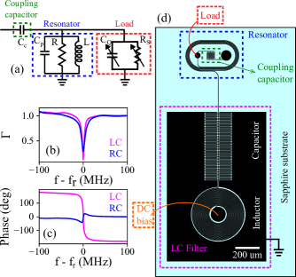
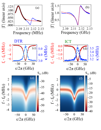
To quantify the improvement provided by the addition of the filter to the resonator assembly, we connect the resonator to a p-type FDSOI nanowire transistor of large dimensions (10 m wide 120 nm long 8 nm high) to simulate a variable load impedance. The device has the same gate stack as the QD devices to be studied later: a 1.3 nm equivalent oxide thickness of high- HfSiON gate dielectric and a combination of 5 nm thick TiN and 50 nm polycrystalline silicon layers as the gate metal. We then characterise the resonance using a vector network analyser (VNA) inside a pumped helium system at 2 K. We measure the resonator assembly in two different configurations and compare the results: (i) DC bias applied through the filter (orange dashed square) and (ii) DC bias applied through a surface mount low pass filter ( pF and k) bonded to the load side of the inductor (effectively bypassing the filter). We plot the magnitude () and phase of the reflection coefficient in the two resonator configurations in Fig. 1b and c (pink and blue traces, respectively). From the plots, we extract the loaded and internal quality factors for case i(ii) of and , respectively. We observe an improvement of a factor of 3 indicating the positive impact of the filter in reducing internal losses. Furthermore, although not represented in the plot, we note a higher resonance with the filter (2059 MHz vs 1880 MHz) which can be attributed to the filter capacitance resulting in a reduction in the effective inductance of the resonator, . For a detailed derivation see Appendix B. As we shall see in the later part of this Article, we observe larger quality factors when testing the assembly with smaller transistors at millikelvin temperatures. Such difference can be explained by (i) the larger area, and hence loss, of the transistors used in this preliminary study and (ii) the TiN layer of the gate stack turning superconducting at K.
III Dispersive Interaction
In this Section, we explore the dispersive interaction between the microwave resonator and QDs in a silicon nanowire transistor, see Fig. 2a. We select a resonator with an effective of 31 nH, a of 40 fF and a (including that of the silicon chiplet) of 140 fF resulting in a resonance frequency of 2116 MHz and a resonator impedance . We connect the resonator to a single gate SOI nanowire transistor with a channel width of 120 nm, a length of 60 nm and height of 8 nm, and a Boron channel doping density of cm-3. We use additional filters (part superconducting chiplet) on the source and drain electrodes. We use the back-gate voltage as well as the top-gate voltage to bias the device to an ICT between a corner dot [50, 51] and a Boron acceptor with overall charge configurations (N+1D, 0B) to (ND,1B), see Fig. 2b. Here, we plot the normalised resonator phase shift. Besides, we see signal at the DRT of the corner dot. We choose this voltage region for its low charge noise.
We characterise the ICT and DRT at the measurement points indicated by the dashed lines and find gate lever arms and , extracted from Landau-Zener-Stückelberg interferometry [52, 53]. We extract the tunnel coupling and tunnel rate of the ICT and DRT, respectively from their transition linewidth [46, 54] and obtain = 15.6 0.4 GHz for the ICT and = 10.2 0.2 GHz for the DRT.
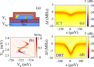
Next, in Fig. 2c,d, we measure the resonator’s dispersive shift induced by the ICT and DRT. To vary the detuning from the charge transition point, we change the top gate voltage. We fit the resonance at each point in detuning to extract the resonant frequency and line-width, . Away from the charge transitions, we extract a bare resonator frequency of GHz with linewidth MHz ( MHz). We find a frequency shift of 1.8 MHz for the ICT and 5.6 MHz for the DRT. Further, for the ICT, we extract a coherent coupling rate MHz, a charge decoherence rate of GHz and a tunnel coupling GHz that closely matches the value extracted from lineshape analysis. For more details on the extraction of parameters from these fits, see Appendix C. In both cases, is of the order of which is the condition for maximum state visibility ( for the ICT and 1.8 for the DRT) [44]. We exploit this regime for fast readout.
IV MEASUREMENT TIME: DRT and ICT
We now characterise the dispersive readout performance on the DRT and the ICT. To quantify the performance, we utilize the power SNR of the transitions at a given integration time, . The measurements at the DRT represent the expected charge readout performance of a SEB [34, 55, 56, 11, 57] while the measurements at the ICT are equivalent to the expected charge readout performance in Pauli-spin blockade-based schemes [58, 59, 60, 61, 62].
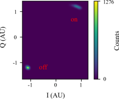
To extract the signal, we measure the difference in the IQ resonator response on and off the DRT (or ICT) peak. We first tune the device on (off) the measurement point, followed by a wait period (100 s) much longer than the bandwidth of the DC line to stabilise the gate voltage and pre-condition the resonator, removing effects due to resonator ring-up. We then integrate the response for . We present the results in Fig. 3a where we plot a 2D histogram of the outcome of 1000 measurements where the IQ signal has been integrated for 100 ns. We observe two well-defined Fresnel lollipops with 2D standard deviation which allows defining the SNR,
| (1) |
We note that at low integration times, as in panel (a), the noise level for both states is equal and set by the cryogenic amplifier. Next, in Fig. 3b, we explore the dependence of the SNR with . To do this, we measure the signal using a sampling rate of 250 MHz (4 ns per point) with a total measurement time of 4 s, to measure the low end of the range, followed by a second measurement with a sampling rate of 5 MHz and total measurement time of 500 s that covers the large range. We then use a moving average to generate data at various effective . Each data point is composed of 1,000 shots on and off the ICT and DRT. We see that at low , the SNR follows the expected linear relationship for white noise-dominated data set by [63]
| (2) |
where relates to the bandwidth of the measurement set-up and corresponds to the integration time for SNR (at large measurement bandwidth) which we used as a characteristic figure of merit [29]. Besides, is determined by the noise type with = 1 corresponding to white noise and 1 for pink and red noise.
At high (red regime Fig. 3b), the data deviates from the linear trend and the SNR increases at a lower rate, characterised by 1. This can be explained by a transition from white noise to 1/ noise-dominated spectrum with a corner frequency around 1 MHz, see Appendix D showing the distortion of the on-state Fresnel lollipop due to excess noise. At very low (pink regime Fig. 3b), we also find a deviation from the linear trend which can be attributed to a finite bandwidth of the measurement setup on the order of 2 ns, matching well the bandwidth of the IQ demodulator at 275 MHz.
By fitting the low regime to Eq. 2 with , we extract a ns for the ICT and ns for the DRT. To our knowledge, the DRT readout figure represents the lowest reported using a multi-module assembly and approaches the best reported values for monolithic resonator integration (1.8 ns [38]) and SET readout (0.625 ns [64]). The ICT figure also comes near to those reported in the literature [44, 65].
Additionally, in panel b, we plot the measurement infidelity, i.e. the likelihood of mislabelling the state of the system. The electrical infidelity is directly related to the SNR via,
| (3) |
where and are the electrical fidelity and infidelity respectively and erf is the error function. We achieve an electrical infidelity of at 53 7 (280 70) ns for the DRT(ICT). Similarly, we achieve an infidelity of at 0.12 0.03 (0.6 0.2) s for the DRT(ICT). We stress that this is the electrical infidelity corresponding to electrical readout errors associated to the quality of the sensor only. When used for qubit state read-out, state decay ( processes) can also introduce readout errors [66]. In any case, for a given , a shorter measurement time reduces the likelihood of state decay and therefore improves fidelity.
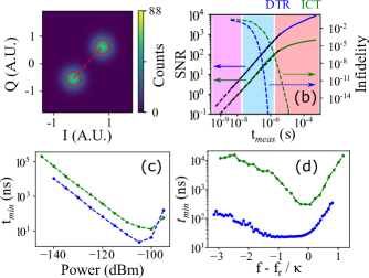
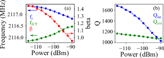
Using as a figure of merit for comparison [29], we now characterise the read-out performance against measurement power and frequency (Fig. 3c and d). For the measurement power, we find decreases for increasing power until it reaches a minimum at -100 dBm and -105 dBm for the ICT and DRT, respectively. This trend can be explained by noting that the signal strength is proportional to the number of photons populating the resonator. However, at intermediate powers, photon back-action causes a broadening of the line-width which reduces the dispersive frequency shift on the resonator, reducing the difference between the on and off states [67]. Finally, at high powers, the large driving induces increased kinetic inductance and losses in the resonator, decreasing its quality factor and therefore reducing its sensitivity (see. Appendix E).
Next, in Fig. 3d, we measure as a function of frequency and fixed power (below power broadening levels). Under these conditions, the frequency shift caused by the charge transition is that shown in Fig. 2c. We find that exhibits a plateau, where its value is minimum, within the frequency range between the bare and loaded frequency of the resonator, a frequency bandwidth of the order of . We note that when applying higher powers, close to the optimal, decreases and therefore narrows the optimal frequency window. The optimum read-out frequency for high power narrows down around the bare resonance frequency (Cochrane et al. in preparation).
V Charge noise measurements
Having characterised the large SNR of the resonator, we now utilize it to determine the charge noise spectrum of the device. Particularly, we study charge noise at the ICT. Charge noise results in time-dependent variations of both the detuning and tunnel coupling between QDs impacting the fidelity of qubit operations [45]. Understanding its magnitude and frequency dependence is hence of high relevance to determine device quality. Charge noise is typically characterised in terms of the detuning noise spectral density () which follows a power law dependence given by
| (4) |
where is the characteristic charge noise at 1 Hz and the exponent is typically around 1 with values ranging between 0.5 and 2 [68]. The power law dependence arises by considering an ensemble of two-level fluctuators (TLFs) with a uniform distribution of activation energies and interactions between them. Typically, charge noise is measured in the frequency range around 1 Hz and quoted in terms of the characteristic value . However, measuring charge noise at high frequencies is essential to determine whether the power law observed at low frequencies extends to the regime at which qubit operations occur. Here, we utilize the resonator to cover charge noise over 9 decades of frequency extending up to 500 kHz, see Fig 4. To cover the frequency range, we utilize two methods: peak tracking and voltage spectroscopy [69].
Peak tracking (bottom left insert) operates by repeatedly measuring the voltage at which the peak of the charge transition occurs. The voltage noise spectral density () is then translated into the detuning noise spectral density by using the ICT lever arm: . We use peak tracking to cover the range to Hz. Voltage spectroscopy (top right insert) quantifies the voltage signal fluctuations at a fixed detuning point, in this case the signal in quadrature () at the point of highest derivative. The detuning noise spectral density can then be calculated as where is the quadrature voltage noise spectral density. We use voltage spectroscopy in the regime from to Hz.
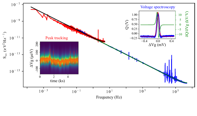
We fit Eq. 14 to the peak tracking and voltage-spectroscopy data. We include a functional modification to the equation to account for aliasing due to finite sampling rate that becomes apparent as an upward bend at the high frequency end of both datasets (See Appendix F). We find a charge noise of 3.9(4.0) eV/ and exponent of 0.99(0.99) for the peak tracking (voltage spectroscopy) method. We note that in the low frequency regime of the peak-tracking below Hz the charge noise drops off which may be due to the dominant effect of one or more TLFs with characteristic frequency below Hz.We recall that the measurement location was partially chosen due to its low charge noise. We additionally measure charge noise at other combinations of gate and back-gate voltages of the device (not shown) and find values in the range of 4.0 - 10 eV/.
The charge noise figure demonstrated here is larger than the state-of-the-art for an MOS structure (0.61 eV [24]) but is within the values reported for other SiO2-only oxide nanowire transistors and below the figure in the few-electron limit [70]. We highlight that the oxide in our sample is composed of 0.8 nm SiO2 and 1.9 nm HfSiON. Such high- dielectrics have been associated with a high oxide trap density which could negatively impact the charge noise figure [51]. Our result demonstrates that high- oxides are not necessarily worse than SiO2-based devices while they provide tighter control of the QD electrostatics manifested in the large gate lever arms reported for high- technology [71, 48].
With the high SNR demonstrated here and the combination of the two methods, we cover the charge noise spectrum over 9 decades of frequency going up to 500 kHz, an upper frequency range comparable to qubit operation rates. Previous work measured charge noise over 5 decades and up to 1 Hz using a combination of current spectroscopy, peak-tracking and variations in charge dephasing exchange control experiments [69]. Struck et al. [68] measured the charge noise of an SET over 9 decades of frequency up to 10 kHz using current spectroscopy. Finally, CPMG methods have been used to study the impact of charge noise on qubit properties for frequencies up to 320 kHz [45] and 2 MHz [72]. Overall, our work demonstrates an easy to use method to study charge noise at the important high frequency end which is relevant to individual qubit operations and directly at the ICT without the need of separate charge sensors that may contribute to the charge noise figure. Besides, our approach may facilitate device quality characterisation and setup noise debugging at high frequencies without the need to resort to qubit measurements. More particularly, we find several reproducible noise sources in the range of 20-100 kHz which we could be caused by mechanical vibrations generated by the pumping system.
VI Discussion
In this Article, we have achieved state-of-the-art charge readout rates utilizing a multi-module microwave assembly. To facilitate the discussion of our results, we will introduce the dependence of with system variables as calculated for small dispersive signals and large tunnel rates [11],
| (5) |
where is the noise temperature.
First of all, with the capacitively coupled microwave assembly, we have looked to comparatively increase the resonator frequency over other multi-module approaches while keeping control over the external coupling, . Secondly, we have introduced an integrated filter on the gate line to increase the quality factor of the resonator and obtained an improvement in of 2.2(3.2). Our data follows a similar trend to results on high frequency (6-8 GHz), high-impedance ( k) distributed wave-guide resonators [73, 74] that showed an improvement of one order of magnitude. To understand the lower improvement factor, we refer to the expression of the microwave photon leak rate through the DC lines () [75, 74]: , where the impedance of the DC line and is the capacitance from the resonator to the DC line. The aim of the filter has been to reduce the a microwave photon experiences towards the DC line. The comparatively lower improvement in our case could be attributed to the lower and , making a less prominent loss mechanism.
To benchmark our results against the reports in literature, we use the figure of merit of . We note that the metric is load aware due to the lever arm, (see Eq. 5). Across the field, there are large differences in ranging from values close to , particularly thin SOI devices [48], to much smaller values , for example, in Si/SiGe quantum wells [22]. To facilitate a resonator-only comparison, we suggest an additional load-agnostic metric: . This choice of metric has two benefits: (i) It allows a better comparison of read-out performance of different resonator across different platforms and (ii) it gives a tool to estimate how well a particular superconducting chiplet would perform on a different quantum system. In Table 1, we show a non-exhaustive list of reflectometry based read-out results of QD systems extracted from the literature.
| Reference | Platform | Sensor type | Resonator type | (ns) | (ns) | |
|---|---|---|---|---|---|---|
| This work | Si-SOI nanowire | SEB | Multi-module | 2.77 | 0.72 | 1.44 |
| In-situ | Multi-module | 13.5 | 0.53 | 3.79 | ||
| Borjans et al. [38] | Si/SiGe | SEB | On-chip | 1.8 | 0.1x | 0.018x |
| Oakes, Ciriano-Tejel et al. [11] | Si-SOI nanowire | SEB (JPA on) | Multi-module | 100 | 0.35 | 12 |
| SEB (JPA off) | Multi-module | 450 | 0.35 | 55 | ||
| Si-SOI nanowire | SEB | Multi-module | 170 | 0.4 | 27 | |
| House et al. [34] | P donor is Si | SEB | Multi-module | 550 | 0.45 | 111 |
| Hogg et al. [57] | P donor is Si | SEB | Multi-module | 720 | 0.38 | 104 |
| Stehlik et al. [65] | InAs nanowire | In-situ (JPA on) | On-chip | 7 | 0.15* | 0.16* |
| In-situ (JPA off) | On-chip | 16000 | 0.15* | 360* | ||
| Ibberson et al. [44] | Si-SOI nanowire | In-situ | Multi-module | 10 | 0.72 | 5.2 |
| Schaal et al. [49] | Si-SOI nanowire | In-situ (JPA on) | Multi-module | 80 | 0.36 | 10.4 |
| In-situ (JPA off) | Multi-module | 1200 | 0.36 | 156 | ||
| Zheng et al. [39] | Si/SiGe | In-situ | On-chip | 170 | Not given | - |
| Keith et al. [64] | P donor is Si | SET | Multi-module | 0.625† | NA | - |
| Noiri et al. [10] | Si/SiGe | SET | Multi-module | 22 † | NA | - |
| House et al. [34] | P donor is Si | SET | Multi-module | 55 | NA | - |
First of all, we see that both the SEB and in-situ readout demonstrations in this Article perform near the state-of-the-art in terms of . Besides, we note that, in our work, at the DRT and the ICT differ by a factor of about 2.6. This difference, not captured in Eq. 5, could be attributed to the increase in photon loss rate at the DRT ( = 2.5 MHz) compared to the ICT ( = 0.5 MHz), which can be understood as a resistive component to the signal, adding on top of the capacitive one.
While both the SEB and in-situ readout results display approaching the state-of-the-art, a comparison through shows that on-chip microwave resonators are ultimately a better choice in terms of enabling high measurement rates for a given technology. This can be particularly appreciated in the SEB results in SiGe [38]. The confined geometry, use of high quality substrates and the use of high kinetic inductance materials should enable higher frequency, and impedance. However, the impact on-chip resonators have on quantum processor topology is not negligible and they come with the additional complexity of hybrid superconductor-semiconductor fabrication. For example, we note that in-situ readout results with on-chip resonators have only reported a higher performance when in conjunction with a Josephson Parametric Amplifier (JPA) which has the role of reducing [65]. In this context, a JPA in conjunction with the multi-module microwave assembly presented here could result in a reduction factor of 20 in , given the typical noise temperature of state-of-the-art cryogenic amplifiers () and the frequency and temperature ( mK) of operation of our system.
Finally, we also benchmark our results against the most sensitive charge sensor to date: the rf-SET. Particularly, we see that the SEB demonstrated here ( ns) approaches the best result for the SET, 625 ps [64], supporting the idea that dispersive readout methods could be as sensitive as dissipative ones [11]. In more detail, it was recently theoretically proposed that the signal generated by the single-electron AC currents in the SEB, when driven at high frequencies, could become of the order of the large single-electron currents flowing through SETs, resulting in comparable sensitivities under the same system noise levels. Furthermore, it was proposed that JPAs could reduce the noise levels more efficiently in dispersive systems given that the ultimate noise source, the Sisyphus noise [77], can be made smaller that the SET’s shot noise. The results in this Article support this theory and encourage further measurements combining high-frequency strongly-coupled SEBs in conjunction with quantum-limited amplification. We also note that progress in dispersive readout methods over SETs would benefit the development of compact quantum processor topologies. In particular, dissipative charge sensors like the SET require three physical contacts additional to the qubit to be sensed, whereas the SEB just requires two. In the case of in-situ readout only the two electrodes controlling a double QD system are needed to implement the method.
VII Conclusion
In conclusion, we have shown the design of a multi-module resonance circuit containing an integrated capacitive coupling element, a spiral inductor and low-pass filters to the bias lines. We use the resonant module in conjunction with a Si-nanowire transistor to achieve a resonance frequency and in excess of 2 GHz and 1600, respectively. We detect QD DRTs and QD-Boron ICTs and operate these as SEB and in-situ dispersive readout, respectively. We find a large SNR resulting in the lowest so far reported for dispersively detected charge sensors using a multi-module assembly and approaching the state-of-the-art of the monolithically integrated resonators and that of the SET. Finally, we use the large SNR to measure the charge noise of the ICT over 9 orders of magnitude up to 500 kHz using purely voltage spectroscopy. This work pushes the limits of charge sensitivity using dispersive readout and provides a transferable platform to improve the sensitivity of other charge-based quantum systems. The improvement in read-out sensitivity will directly impact the achievable read-out time and state fidelity of semiconductor spin qubit systems helping in the development of a fault-tolerant quantum computer.
Acknowledgement
This research was supported by European Union’s Horizon 2020 research and innovation programme under grant agreement no. 951852 (QLSI), and by the UK’s Engineering and Physical Sciences Research Council (EPSRC) via the Cambridge NanoDTC (EP/L015978/1). F.E.v.H. acknowledges funding from the Gates Cambridge fellowship (Grant No. OPP1144). L.C. acknowledges funding from EPSRC Cambridge UP-CDT EP/L016567/1. J. W. A. R. acknowledges funding from the EPSRC Core-to-Core International Network Grant “Oxide Superspin” (No. EP/ P026311/1). M.F.G.Z. acknowledges a UKRI Future Leaders Fellowship [MR/V023284/1].
Appendix A Design details of superconducting resonator and filter
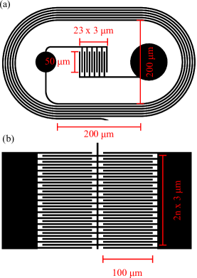
In this section, we discuss the design of the inductance and capacitance values of the superconducting resonator and how these translate into its physical dimensions. Given an estimate of the parasitic capacitance on the load chip of the order of 200 fF, we targeted inductances on the order of 20-40 nH to achieve a GHz. Given an estimate of parasitic losses of the circuit between 0.1 - 1 M we calculated the required coupling capacitor for the matching condition [)] between 10-40 fF.
In order to estimate the inductance and capacitance of the various circuit elements, we used AWR Microwave Office, a finite element RF simulator, to simulate the elements before fabrication. We designed spiral inductors with an elongated middle section to create space for the coupling capacitor (see Fig. 5a). There are no simple, analytical equations for the inductance of such spiral inductors. Nevertheless, the inductance can be guided by equations for circular spiral inductors, namely where is the number of turns and is the diameter [78]. In our designs, we fixed the inner diameter to 200 m with a horizontal elongation of 200 m and used as a tuning parameter to select the inductance.
For the coupling capacitor and filter capacitor, we made use of interdigitated capacitors (Fig. 5a and b). The capacitance of these can be predicted using conformal mapping techniques [79]. For design purposes, it is useful to note that the capacitance is approximately linear with the number and length of fingers of the capacitor. To keep the designs between resonators with different as similar as possible, we fixed the finger length to 50 m and varied the number of fingers between 4 and 16 to achieve a capacitance of 10-40 fF. For the filter capacitor, we set the finger length to 100 m instead and used 100 fingers on either side of the capacitor to get to a capacitance of 1 pF.
A final set of parameters are the track width () and separation (). In general, lower values of and make the designs smaller leading to lower parasitic capacitances to ground and smaller footprints, however they can also make fabrication more challenging and increase capacitance between adjacent turns of the inductor. Finally, if there are impurities in the substrate these can couple more strongly with confined electric fields between features with smaller and therefore reduce the of the resonator. For our designs, we chose 3 m for and .
Appendix B Inductance correction for a finite filter capacitor

For a capacitively coupled resonator with a filter capacitor behind the inductor (Fig. 6a), it can be shown that in the limit of the negligible resistances the resonance frequency, , is given by
| (6) |
where , , , are the inductance, coupling capacitance, resonator capacitance and filter capacitance respectively. Noting that the resonance frequency without is given by the first term, we can see that the resonance frequency is corrected upwards by a factor depending on how large the filter capacitance is with respect to the bare capacitance of the circuit. Intuitively, this can be understood by analysing the impedance of the inductor in series with the filter capacitor (Fig. 6b) and therefore calculating an effective inductance given by
| (7) | |||
| (8) |
Inserting Eq. 6 at resonance when this simplifies to:
| (9) |
where the approximation holds for . We have shown that introduce a correction term to which can be understood as a reduction of the effective inductance of the resonator.
Appendix C Fitting dispersive shift
In order to fit the dispersive shift caused by the ICT, we first need to accurately determine the resonance frequency and bandwidth at each point of detuning. The first task is to remove the background of the frequency spectrum caused by standing waves in the RF circuitry of the refrigerator (see Fig. 7a). To do so, we plot the reflected magnitude in linear axes and then fit a Lorentzian background to the reflection spectrum away from the resonance frequency. We subtract this background from the reflection spectrum in dB axes.
The asymmetry of the remaining resonance is characteristic of a interferences between the signal reflected from the resonator with that reflected from other boundaries, potentially due to the RF components at the mixing chamber. This can be modelled by taking the external factor to be complex of the form [80]:
| (10) |
where is the resonance depth, and , and the coupling coefficient is used as a fixed parameter extracted from the resonance depth using , for an undercoupled resonator, and for an overcoupled resonator. Based on this, we extract the frequency shift and linewidth of the resonator as a function of detuning (Fig. 7c and d).
In the case of the ICT, the frequency shift can be modelled by a dispersive shift caused by a charge qubit onto the resonator described by the Hamiltonian [44]:
| (11) |
where is the frequency detuning from the resonance frequency , is the resonator-qubit detuning with the qubit frequency , = is the effective charge coupling rate. The shift in resonance frequency and are given by
| (12) | |||
| (13) |
where is the shifted resonance frequency as a function of detuning, is the bare photon loss rate and and is the charge qubit decoherence.
Appendix D Effect of charge noise on Fresnel blobs
In the high- regime of the SNR measurements (Fig. 3b), we see a reduction in the rate of increase of the SNR. This can be attributed to a change in the noise characteristic of the measurement, changing the exponent in Eq. 1. At low the noise is white noise (cryogenic amplifier), leading to a noise power dependence of 1/ arising from sampling from a normal distribution around a mean, and therefore a SNR . At large , excess noise manifest reducing the SNR. This can be demonstrated by plotting the Fresnel blobs of a measurement at large (Fig. 8). Note how the on-state measurement, being detuning dependent, shows a significant elongation of the blob while the off-state blob remains mostly unaffected.
The two main sources of added noise are due to detuning () and tunnel noise ( or ). Changes in detuning shift the measurement point away from the centre of the peak which reduces the signal. As the slope of the signal with detuning is zero at (see Fig.4 upper right insert), the signal is to first order insensitive to detuning noise. Tunnel noise can couple directly into the signal by changing the peak height, however is often less severe. Coincidentally, voltage spectroscopy is also sensitive to tunnel noise and therefore the difference in the noise characteristic from peak tracking (3.9 eV) and voltage spectroscopy (4.0 eV) can be used to demonstrate this.
Appendix E Kinetic inductance and losses introduced in resonator by large RF driving power
At large driving powers, breaking of Cooper pairs can lead to an increased kinetic inductance as well as additional losses in the resonator. The kinetic inductance shifts the resonance frequency down, while the losses reduce and therefore reduce the coupling constant .
To analyse this effect we measure the frequency spectrum of the resonator near the ICT as a function of power. We plot , , and in Fig. 9. Additionally, we also plot the shifted by the ICT which displays a reduced shift due to photon back-action. We find a decrease in by 0.56 MHz between -115 to -90 dBm of power which constitutes an inductance change of 16 3 pH assuming a purely inductive change.
We also find a monotonic decrease in with power, affecting the impedance matching . We find critical coupling = 1 at a power of -91.5 dBm. Note that this is significantly above the optimum read-out power found in this work.
Appendix F Aliasing effect of finite sampling on charge noise
When taking the Fourier transform of a sampled data set, duplicates of the Fourier spectrum are created in frequency space that are separated by the sample frequency . In a non-ideal situation this will create an overlap between the true frequency spectrum and it’s duplicates, an effect known as aliasing. This effect can be effectively avoided if the frequency spectrum of the data has a frequency cut-off, , which is less or equal than half the , known as the Nyquist condition, i.e. . Meeting the Nyquist condition can be effected by increasing the sample rate or using a low-pass filter.
In Fig. 4, we find an upwards bend in the charge noise data, in the range f 10-1 for the peak tracking and the range f 105 for the voltage spectroscopy. We attribute this to an artefact caused by the aliasing effect described above. In principle this can be avoided by implementing a low-pass filter before the data is sampled, however depending on the frequency drop-off of the filter there may still be a finite contribution to the charge noise. The finite noise contribution can be modelled by a duplication of the charge noise offset by a frequency equal to the sampling frequency :
| (14) |
In the case of our voltage-spectroscopy measurement we sampled at a frequency of 1 MHz, using a low-pass filter of 100 kHz with 6 dB drop-off per decade (implemented by Stanford Research SR560 pre-amplifiers with variable low-pass filter), fulfilling the Nyquist condition. Because of the presence of this filter there is much less of an aliasing effect in the voltage-spectroscopy spectrum (compared to that of the peak-tracking) but some amount remains above 100 kHz.
For the peak-tracking, on the other hand, there is effectively no filtering in the relevant frequency range. Peak positions are sampled at an of 10.4 Hz (given by the speed of the voltage ramp of 83.33 Hz over 8 averages) and the low-pass filter of the SR560 is set at 10 kHz. Reducing the low pass-filter frequency will interfere with the peak shape and therefore make accurate determination of the peak location impossible. This makes it difficult to remove any aliasing contribution for charge noise obtained using the peak-tracking method.
References
- Petta et al. [2005] J. R. Petta, A. C. Johnson, J. M. Taylor, E. A. Laird, A. Yacoby, M. D. Lukin, C. M. Marcus, M. P. Hanson, and A. C. Gossard, Science 309, 2180 (2005).
- Persson et al. [2010] F. Persson, C. M. Wilson, M. Sandberg, G. Johansson, and P. Delsing, Nano Lett. 10, 953 (2010).
- Veldhorst et al. [2015] M. Veldhorst, C. H. Yang, J. C. C. Hwang, W. Huang, J. P. Dehollain, J. T. Muhonen, S. Simmons, A. Laucht, F. E. Hudson, K. M. Itoh, A. Morello, and A. S. Dzurak, Nature 526, 410 (2015).
- Hendrickx et al. [2021] N. W. Hendrickx, W. I. L. Lawrie, M. Russ, F. van Riggelen, S. L. de Snoo, R. N. Schouten, A. Sammak, G. Scappucci, and M. Veldhorst, Nature 591, 580 (2021).
- Zhou et al. [2022] X. Zhou, G. Koolstra, X. Zhang, G. Yang, X. Han, B. Dizdar, X. Li, R. Divan, W. Guo, K. W. Murch, D. I. Schuster, and D. Jin, Nature 605, 46 (2022).
- Bluhm et al. [2011] H. Bluhm, S. Foletti, I. Neder, M. Rudner, D. Mahalu, V. Umansky, and A. Yacoby, Nat. Phys. 7, 109 (2011).
- Veldhorst et al. [2014] M. Veldhorst, J. Hwang, C. Yang, L. A.W., B. de Ronde, J. P. Dehollain, J. Muhonen, F. Hudson, K. Itoh, A. Morello, and A. S. Dzurak, Nature 9, 981 (2014).
- Spietz et al. [2003] L. Spietz, K. W. Lehnert, I. Siddiqi, and R. J. Schoelkopf, Science 300, 1929 (2003).
- Connors et al. [2020] E. J. Connors, J. Nelson, and J. M. Nichol, Phys. Rev. Appl. 13, 024019 (2020).
- Noiri et al. [2020] A. Noiri, K. Takeda, J. Yoneda, T. Nakajima, T. Kodera, and S. Tarucha, Nano Lett. 20, 947 (2020).
- Oakes et al. [2023] G. A. Oakes, V. N. Ciriano-Tejel, D. F. Wise, M. A. Fogarty, T. Lundberg, C. Lainé, S. Schaal, F. Martins, D. J. Ibberson, L. Hutin, B. Bertrand, N. Stelmashenko, J. W. A. Robinson, L. Ibberson, A. Hashim, I. Siddiqi, A. Lee, M. Vinet, C. G. Smith, J. J. L. Morton, and M. F. Gonzalez-Zalba, Phys. Rev. X 13, 011023 (2023).
- Pearson et al. [2021] A. N. Pearson, Y. Guryanova, P. Erker, E. A. Laird, G. A. D. Briggs, M. Huber, and N. Ares, Phys. Rev. X 11, 021029 (2021).
- Chawner et al. [2021] J. Chawner, S. Barraud, M. Gonzalez-Zalba, S. Holt, E. Laird, Y. A. Pashkin, and J. Prance, Phys. Rev. Appl. 15, 034044 (2021).
- Blanchet et al. [2022] F. Blanchet, Y.-C. Chang, B. Karimi, J. T. Peltonen, and J. P. Pekola, Phys. Rev. Appl. 17, L011003 (2022).
- Ono et al. [2002] K. Ono, D. Austing, Y. Tokura, and S. Tarucha, Science 297, 1313 (2002).
- Elzerman et al. [2004] J. M. Elzerman, R. Hanson, L. H. W. van Beveren, B. Witkamp, L. M. K. Vandersypen, and L. P. Kouwenhoven, Nature 430, 431 (2004).
- Fowler et al. [2012] A. G. Fowler, M. Mariantoni, J. M. Martinis, and A. N. Cleland, Phys. Rev. A 86, 032324 (2012).
- Xue et al. [2022] X. Xue, M. Russ, N. Samkharadze, B. Undseth, A. Sammak, G. Scappucci, and L. M. K. Vandersypen, Nature 601, 343 (2022).
- Noiri et al. [2022] A. Noiri, K. Takeda, T. Nakajima, T. Kobayashi, A. Sammak, G. Scappucci, and S. Tarucha, Nature 601, 338 (2022).
- Mills et al. [2022] A. R. Mills, C. R. Guinn, M. J. Gullans, A. J. Sigillito, M. M. Feldman, E. Nielsen, and J. R. Petta, Sci. Adv. 8, eabn5130 (2022).
- Takeda et al. [2022] K. Takeda, A. Noiri, T. Nakajima, T. Kobayashi, and S. Tarucha, Nature 608, 682 (2022).
- Philips et al. [2022] S. G. J. Philips, M. T. Madzik, S. V. Amitonov, S. L. de Snoo, M. Russ, N. Kalhor, C. Volk, W. I. L. Lawrie, D. Brousse, L. Tryputen, B. P. Wuetz, A. Sammak, M. Veldhorst, G. Scappucci, and L. M. K. Vandersypen, Nature 609, 919 (2022).
- Maurand et al. [2016] R. Maurand, X. Jehl, D. Kotekar-Patil, A. Corna, H. Bohuslavskyi, R. Laviéville, L. Hutin, S. Barraud, M. Vinet, M. Sanquer, and S. De Franceschi, Nat. Commun. 7, 13575 EP (2016).
- Elsayed et al. [2022] A. Elsayed, M. Shehata, C. Godfrin, S. Kubicek, S. Massar, Y. Canvel, J. Jussot, G. Simion, M. Mongillo, D. Wan, B. Govoreanu, I. P. Radu, R. Li, P. V. Dorpe, and K. D. Greve, Low charge noise quantum dots with industrial cmos manufacturing (2022), arXiv:2212.06464 [cond-mat.mes-hall] .
- Zwerver et al. [2022] A. M. J. Zwerver, T. Krähenmann, T. F. Watson, L. Lampert, H. C. George, R. Pillarisetty, S. A. Bojarski, P. Amin, S. V. Amitonov, J. M. Boter, R. Caudillo, D. Correas-Serrano, J. P. Dehollain, G. Droulers, E. M. Henry, R. Kotlyar, M. Lodari, F. Lüthi, D. J. Michalak, B. K. Mueller, S. Neyens, J. Roberts, N. Samkharadze, G. Zheng, O. K. Zietz, G. Scappucci, M. Veldhorst, L. M. K. Vandersypen, and J. S. Clarke, Nat. Electron. 5, 184 (2022).
- Xue et al. [2021] X. Xue, B. Patra, J. P. G. van Dijk, N. Samkharadze, S. Subramanian, A. Corna, B. P. Wuetz, C. Jeon, F. Sheikh, E. Juarez-Hernandez, B. P. Esparza, H. Rampurawala, B. Carlton, S. Ravikumar, C. Nieva, S. Kim, H.-J. Lee, A. Sammak, G. Scappucci, M. Veldhorst, F. Sebastiano, M. Babaie, S. Pellerano, E. Charbon, and L. M. K. Vandersypen, Nature 593, 205 (2021).
- Ruffino et al. [2022] A. Ruffino, T.-Y. Yang, J. Michniewicz, Y. Peng, E. Charbon, and M. F. Gonzalez-Zalba, Nat. Electron. 5, 53 (2022).
- Gonzalez-Zalba et al. [2021] M. F. Gonzalez-Zalba, S. de Franceschi, E. Charbon, T. Meunier, M. Vinet, and A. S. Dzurak, Nat. Electron. 4, 872 (2021).
- Vigneau et al. [2022] F. Vigneau, F. Fedele, A. Chatterjee, D. Reilly, F. Kuemmeth, F. Gonzalez-Zalba, E. Laird, and N. Ares, Probing quantum devices with radio-frequency reflectometry (2022), arXiv:2202.10516 [cond-mat.mes-hall] .
- Veldhorst et al. [2017] M. Veldhorst, H. G. J. Eenink, C. H. Yang, and A. S. Dzurak, Nat. Commun. 8, 1766 (2017).
- Vandersypen et al. [2017] L. M. K. Vandersypen, H. Bluhm, J. S. Clarke, A. S. Dzurak, R. Ishihara, A. Morello, D. J. Reilly, L. R. Schreiber, and M. Veldhorst, Npj Quantum Inf. 3, 34 (2017).
- Li et al. [2018] R. Li, L. Petit, D. P. Franke, J. P. Dehollain, J. Helsen, M. Steudtner, N. K. Thomas, Z. R. Yoscovits, K. J. Singh, S. Wehner, L. M. K. Vandersypen, J. S. Clarke, and M. Veldhorst, Sci. Adv. 4 (2018).
- Crawford et al. [2023] O. Crawford, J. R. Cruise, N. Mertig, and M. F. Gonzalez-Zalba, Npj Quantum Inf. 9, 13 (2023).
- House et al. [2016] M. G. House, I. Bartlett, P. Pakkiam, M. Koch, E. Peretz, J. V. D. Heijden, T. Kobayashi, S. Rogge, and M. Y. Simmons, Phys. Rev. Appl. 6, 044016 (2016).
- Urdampilleta et al. [2019] M. Urdampilleta, D. J. Niegemann, E. Chanrion, B. Jadot, C. Spence, P.-A. Mortemousque, C. Bäuerle, L. Hutin, B. Bertrand, S. Barraud, R. Maurand, M. Sanquer, X. Jehl, S. D. Franceschi, M. Vinet, and T. Meunier, Nat. Nanotechnol. 14, 737 (2019).
- Petersson et al. [2010] K. D. Petersson, C. G. Smith, D. Anderson, P. Atkinson, G. A. C. Jones, and D. A. Ritchie, Nano Lett. 10, 2789 (2010).
- Colless et al. [2013] J. I. Colless, A. C. Mahoney, J. M. Hornibrook, A. C. Doherty, H. Lu, A. C. Gossard, and D. J. Reilly, Phys. Rev. Lett. 110, 046805 (2013).
- Borjans et al. [2021] F. Borjans, X. Mi, and J. Petta, Phys. Rev. Appl. 15, 044052 (2021).
- Zheng et al. [2019] G. Zheng, N. Samkharadze, M. L. Noordam, N. Kalhor, D. Brousse, A. Sammak, G. Scappucci, and L. M. K. Vandersypen, Nat. Nanotechnol. (2019).
- Harvey-Collard et al. [2022] P. Harvey-Collard, J. Dijkema, G. Zheng, A. Sammak, G. Scappucci, and L. M. K. Vandersypen, Phys. Rev. X 12, 021026 (2022).
- Mi et al. [2018] X. Mi, M. Benito, S. Putz, D. M. Zajac, J. M. Taylor, G. Burkard, and J. R. Petta, Nature 555, 599 (2018).
- Yu et al. [2022] C. X. Yu, S. Zihlmann, J. C. Abadillo-Uriel, V. P. Michal, N. Rambal, H. Niebojewski, T. Bedecarrats, M. Vinet, E. Dumur, M. Filippone, B. Bertrand, S. De Franceschi, Y.-M. Niquet, and R. Maurand, Strong coupling between a photon and a hole spin in silicon (2022), arXiv:2206.14082 [cond-mat.mes-hall] .
- Holman et al. [2021] N. Holman, D. Rosenberg, D. Yost, J. L. Yoder, R. Das, W. D. Oliver, R. McDermott, and M. A. Eriksson, Npj Quantum Inf. 7, 137 (2021).
- Ibberson et al. [2021] D. J. Ibberson, T. Lundberg, J. A. Haigh, L. Hutin, B. Bertrand, S. Barraud, C.-M. Lee, N. A. Stelmashenko, G. A. Oakes, L. Cochrane, J. W. Robinson, M. Vinet, M. F. Gonzalez-Zalba, and L. A. Ibberson, PRX Quantum 2, 020315 (2021).
- Yoneda et al. [2017] J. Yoneda, K. Takeda, T. Otsuka, T. Nakajima, M. R. Delbecq, G. Allison, T. Honda, T. Kodera, S. Oda, Y. Hoshi, N. Usami, K. M. Itoh, and S. Tarucha, Nat. Nanotechnol. (2017).
- Mizuta et al. [2017] R. Mizuta, R. M. Otxoa, A. C. Betz, and M. F. Gonzalez-Zalba, Phys. Rev. B 95, 045414 (2017).
- Esterli et al. [2019] M. Esterli, R. M. Otxoa, and M. F. Gonzalez-Zalba, Appl. Phys. Lett. 114, 253505 (2019).
- Ahmed et al. [2018a] I. Ahmed, J. A. Haigh, S. Schaal, S. Barraud, Y. Zhu, C.-m. Lee, M. Amado, J. W. A. Robinson, A. Rossi, J. J. L. Morton, and M. F. Gonzalez-Zalba, Phys. Rev. Appl. 10, 014018 (2018a).
- Schaal et al. [2020] S. Schaal, I. Ahmed, J. A. Haigh, L. Hutin, B. Bertrand, S. Barraud, M. Vinet, C.-M. Lee, N. Stelmashenko, J. W. A. Robinson, , J. Y. Qiu, S. Hacohen-Gourgy, I. Siddiqi, M. F. Gonzalez-Zalba, and J. J. L. Morton, Phys. Rev. Lett. 124, 067701 (2020).
- Voisin et al. [2014] B. Voisin, V.-H. Nguyen, J. Renard, X. Jehl, S. Barraud, F. Triozon, M. Vinet, I. Duchemin, Y.-M. Niquet, S. de Franceschi, and M. Sanquer, Nano Lett. 14, 2094 (2014).
- Ibberson et al. [2018] D. J. Ibberson, L. Bourdet, J. C. Abadillo-Uriel, I. Ahmed, S. Barraud, M. J. Calderón, Y.-M. Niquet, and M. F. Gonzalez-Zalba, Appl. Phys. Lett. 113, 053104 (2018).
- Shevchenko et al. [2010] S. Shevchenko, S. Ashhab, and F. Nori, Phys. Rep. 492, 1 (2010).
- Gonzalez-Zalba et al. [2016] M. F. Gonzalez-Zalba, S. N. Shevchenko, S. Barraud, J. R. Johansson, A. J. Ferguson, F. Nori, and A. C. Betz, Nano Lett. 16, 1614 (2016).
- Ahmed et al. [2018b] I. Ahmed, A. Chatterjee, S. Barraud, J. J. L. Morton, J. A. Haigh, and M. F. Gonzalez-Zalba, Commun. Phys. 1, 66 (2018b).
- Ciriano-Tejel et al. [2021] V. N. Ciriano-Tejel, M. A. Fogarty, S. Schaal, L. Hutin, B. Bertrand, L. Ibberson, M. F. Gonzalez-Zalba, J. Li, Y.-M. Niquet, M. Vinet, and J. J. Morton, PRX Quantum 2, 010353 (2021).
- Niegemann et al. [2022] D. J. Niegemann, V. El-Homsy, B. Jadot, M. Nurizzo, B. Cardoso-Paz, E. Chanrion, M. Dartiailh, B. Klemt, V. Thiney, C. Bäuerle, P.-A. Mortemousque, B. Bertrand, H. Niebojewski, M. Vinet, F. Balestro, T. Meunier, and M. Urdampilleta, PRX Quantum 3, 040335 (2022).
- Hogg et al. [2023] M. Hogg, P. Pakkiam, S. Gorman, A. Timofeev, Y. Chung, G. Gulati, M. House, and M. Simmons, PRX Quantum 4, 010319 (2023).
- Petersson et al. [2012] K. D. Petersson, L. W. McFaul, M. D. Schroer, M. Jung, J. M. Taylor, A. A. Houck, and J. R. Petta, Nature 490, 380 (2012).
- Betz et al. [2015] A. C. Betz, R. Wacquez, M. Vinet, X. Jehl, A. L. Saraiva, M. Sanquer, A. J. Ferguson, and M. F. Gonzalez-Zalba, Nano Lett. 15, 4622 (2015).
- House et al. [2015] M. G. House, K. Kobayashi, B. Weber, S. J. Hile, T. F. Watson, J. van der Heijden, S. Rogge, and M. Y. Simmons, Nat. Commun. 6, 8848 (2015).
- Pakkiam et al. [2018] P. Pakkiam, A. V. Timofeev, M. G. House, M. R. Hogg, T. Kobayashi, M. Koch, S. Rogge, and M. Y. Simmons, Phys. Rev. X 8, 041032 (2018).
- West et al. [2019] A. West, B. Hensen, A. Jouan, T. Tanttu, C.-H. Yang, A. Rossi, M. F. Gonzalez-Zalba, F. Hudson, A. Morello, D. J. Reilly, and A. S. Dzurak, Nat. Nanotechnol. 14, 437 (2019).
- Barthel et al. [2010] C. Barthel, M. Kjærgaard, J. Medford, M. Stopa, C. M. Marcus, M. P. Hanson, and A. C. Gossard, Phys. Rev. B 81, 161308 (2010).
- Keith et al. [2019] D. Keith, M. G. House, M. B. Donnelly, T. F. Watson, B. Weber, and M. Y. Simmons, Phys. Rev. X 9, 41003 (2019).
- Stehlik et al. [2015] J. Stehlik, Y.-Y. Liu, C. M. Quintana, C. Eichler, T. R. Hartke, and J. R. Petta, Phys. Rev. Appl. 4, 014018 (2015).
- Laucht et al. [2021] A. Laucht, F. Hohls, N. Ubbelohde, M. F. Gonzalez-Zalba, D. J. Reilly, S. Stobbe, T. Schröder, P. Scarlino, J. V. Koski, A. Dzurak, C.-H. Yang, J. Yoneda, F. Kuemmeth, H. Bluhm, J. Pla, C. Hill, J. Salfi, A. Oiwa, J. T. Muhonen, E. Verhagen, M. D. LaHaye, H. H. Kim, A. W. Tsen, D. Culcer, A. Geresdi, J. A. Mol, V. Mohan, P. K. Jain, and J. Baugh, Nanotechnology 32, 162003 (2021).
- Derakhshan Maman et al. [2020] V. Derakhshan Maman, M. Gonzalez-Zalba, and A. Pályi, Phys. Rev. Appl. 14, 064024 (2020).
- Struck et al. [2020] T. Struck, A. Hollmann, F. Schauer, O. Fedorets, A. Schmidbauer, K. Sawano, H. Riemann, N. V. Abrosimov, Ł. Cywiński, D. Bougeard, and L. R. Schreiber, Npj Quantum Inf. 6, 40 (2020).
- Kranz et al. [2020] L. Kranz, S. K. Gorman, B. Thorgrimsson, Y. He, D. Keith, J. G. Keizer, and M. Y. Simmons, Adv. Mater. 32, 2003361 (2020).
- Spence et al. [2022] C. Spence, B. Cardoso-Paz, V. Michal, E. Chanrion, D. J. Niegemann, B. Jadot, P.-A. Mortemousque, B. Klemt, V. Thiney, B. Bertrand, L. Hutin, C. Bäuerle, F. Balestro, M. Vinet, Y.-M. Niquet, T. Meunier, and M. Urdampilleta, Probing charge noise in few electron cmos quantum dots (2022), arXiv:2209.01853 [cond-mat.mes-hall] .
- Gonzalez-Zalba et al. [2015] M. F. Gonzalez-Zalba, S. Barraud, A. Ferguson, and A. C. Betz, Nat. Commun. 6, 6084 (2015).
- Connors et al. [2022] E. J. Connors, J. Nelson, L. F. Edge, and J. M. Nichol, Nat. Commun. 13, 940 (2022).
- Mi et al. [2017] X. Mi, J. V. Cady, D. M. Zajac, P. W. Deelman, and J. R. Petta, Science 355, 156 (2017).
- Harvey-Collard et al. [2020] P. Harvey-Collard, G. Zheng, J. Dijkema, N. Samkharadze, A. Sammak, G. Scappucci, and L. M. K. Vandersypen, Phys. Rev. Appl. 14, 034025 (2020).
- Mazin [2005] B. A. Mazin, Microwave Kinetic Inductance Detectors, Ph.D. thesis, California Institute of Technology (2005).
- Jung et al. [2012] M. Jung, M. D. Schroer, K. D. Petersson, and J. R. Petta, Appl. Phys. Lett. 100, 253508 (2012).
- Cochrane et al. [2022] L. Cochrane, A. A. Seshia, and M. F. G. Zalba, Intrinsic Noise of the Single Electron Box (2022), arXiv:2209.15086 [cond-mat.mes-hall] .
- Mohan et al. [1999] S. S. Mohan, M. del Mar Hershenson, S. P. Boyd, and T. H. Lee, IEEE J. Solid-State Circuits 34, 1419 (1999).
- Igreja and Dias [2004] R. Igreja and C. Dias, Sens. Actuator A Phys. 112, 291 (2004).
- Khalil et al. [2012] M. S. Khalil, M. J. A. Stoutimore, F. C. Wellstood, and K. D. Osborn, J. Appl. Phys. 111, 054510 (2012).