Cryogenic Multiplexing with Bottom-Up Nanowires
Abstract
Bottom-up grown nanomaterials play an integral role in the development of quantum technologies. Among these, semiconductor nanowires (NWs) are widely used in proof-of-principle experiments, however, difficulties in parallel processing of conventionally-grown NWs makes scalability unfeasible. Here, we harness selective area growth (SAG) to remove this road-block. We demonstrate large scale integrated SAG NW circuits consisting of 512 channel multiplexer/demultiplexer pairs, incorporating thousands of interconnected SAG NWs operating under deep cryogenic conditions. Multiplexers enable a range of new strategies in quantum device research and scaling by increase the device count while limiting the number of connections between room-temperature control electronics and the cryogenic samples. As an example of this potential we perform a statistical characterization of large arrays of identical SAG quantum dots thus establishing the feasibility of applying cross-bar gating strategies for efficient scaling of future SAG quantum circuits.
Quantum electronics is rapidly maturing towards large scale integrated (LSI) circuits incorporating a multitude of interacting quantum devices. There is therefore an onus on potential quantum materials candidates to exhibit both high-precision reproducibility and scalability potential. Semiconductor nanowires (NWs) constitute an important platform for quantum electronics, since the electronic confinement intrinsic to the structure simplifies fabrication of complex devicesmourik:2012 ; hu:2007 ; hofstetter:2009 ; fasth2005tunable , the flexibility of contact materials enables hybridization with important quantum materials such as superconductors doh:2005 ; xiang:2006 ; hofstetter:2009 ; mourik:2012 ; larsen:2015 ; krogstrup:2015 ; hays:2018 , and an increased capacity for strain relaxation over bulk materials enables exploration of exotic heterostructureshu:2007 ; xiang:2006 ; krogstrup:2015 ; SvenssonNL15 . Conventional NWs grown perpendicular to the substrate have been highly successful for high-performance electronics, simple complementary circuits, and in fundamental mesoscopic physicsfasth2005tunable ; hu:2007 ; doh:2005 ; xiang:2006 ; hofstetter:2009 ; mourik:2012 ; larsen:2015 ; krogstrup:2015 ; hays:2018 ; tomioka:2012 ; SvenssonNL15 . However, the difficulty in fabricating individual vertical devices, and the insufficient precision and yield of techniques for transferring NWs to the planar geometry compatible with standard semiconductor processingfreer:2010a ; yao:2013 ; li:2008 has thus far inhibited development of LSI NW circuits. A promising alternative is the bottom-up growth of in-plane semiconductor NWs directly on a suitable device substrate using selective area growthWang2019Jun ; op2020plane ; Raya2020Jan ; Bollani2020Jan (SAG). In SAG, the positions and dimensions of NWs are controlled by lithographically defining openings in a dielectric mask, enabling the controlled growth of large-scale networks and NW arraysAseev2019Jan ; Krizek2018Sep ; op2020plane . While proof-of-principle single NW devices, e.g., field effect transistors (FETs) beznasyuk:2022 ; Friedl2018Apr , Hall crossesLee2019Aug , quantum interferometersvaitiekenas2018selective ; Krizek2018Sep , hybrid superconducting deviceshertel:2022 ; vaitiekenas2018selective , and quantum dotstenkate:2022 have been reported, scalability towards integrated quantum circuits – a central motivation behind the development of SAG and similar bottom-up grown planar nanostructuresschmid:2015 ; gooth:2017 – has not been addressed.
Here we make the first demonstration of LSI circuits based on SAG. Starting from large arrays of thousands of SAG NWs we fabricate multiplexer (MUX) circuits which operate at the deep cryogenic conditions relevant for quantum electronics. Cryogenic multiplexers are key ingredients towards scaling of quantum electronicspauka:2020 ; paquelet2020multiplexed ; smith:2014 ; smith:2020 as the number of addressable devices scales exponentially – rather than linearly – with the number of connecting control lines. This is crucial for reducing heat load from wiring between the cryogenic sample and room-temperature, and integrated MUX circuits allow highly dense packing of devices utilizing chip-area conventionally required for bonding and routing. Our setup allows us to address and measure 512 individual SAG quantum devices using only 37 control lines. Our architecture also includes de-multiplexers (d-MUX) connected back-to-back with the corresponding MUX, enabling us to unambiguously confirm the functionality of the circuit, to identify faulty operation among the thousands of NWFETs, and self-correct against most failure modes.
Introducing on-chip multiplexing to bottom-up grown nanostructures enables new strategies in quantum electronics research, such as automated searches through large ensembles of devices for rare or exotic phenomena, and systematic, statistically significant exploration of the correlation between device performance and e.g., materials properties or device geometry. To demonstrate the potential of the latter we perform a statistical characterization of device reproducibility within a large array of nominally identical SAG NW quantum dots (QDs). QD arrays are promising candidates for implementing quantum computation and simulationloss1998quantum ; tomioka2020rational ; vandersypen2019semiconductor , and quantifying device-to-device reproducibility – enabled by the MUX circuit – is crucial for the successful development of crossbar gate architectures which constitute an important strategy for limiting gate counts in realistic large scale implementationsli2018crossbar ; Borsoi:2022 . We find that all QDs of the array can be concurrently tuned to Coulomb Blockade using only three shared crossbar gates further confirming the potential SAG as a scalable platform for quantum devices,
Material and electrical properties
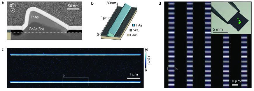
Our circuits are based on \hkl[0-11] oriented InAs SAG NWs grown using molecular beam epitaxy (MBE) on GaAs \hkl(311)A substrates. See Methods and Supplementary Section S1 for details. Figure 1a shows a cross-sectional high-angle annular dark field scanning transmission electron microscope (HAADF STEM) micrograph of a single NW, and Fig. 1b shows a combined schematic and atomic force microscopy (AFM) micrograph of a NW section. The conducting InAs channel sits atop an insulating GaAs substrate and GaAs(Sb) bufferKrizek2018Sep . The NWs are terminated with \hkl111A facets as a consequence of the \hkl(311)A substrate symmetry, producing the asymmetric cross-section. Detailed structural analysis is presented in Supplementary Section S2. Figures 1c and d illustrate the capacity for scale-up inherent to SAG, through an AFM micrograph and dark-field optical microscope micrograph of representative sections of a array of nominally identical m-long NWs. The inset to Fig. 1d shows a photograph of a cleaved piece of the growth wafer containing SAG NWs, of which were used for device fabrication; the diffraction from the large arrays is visible.
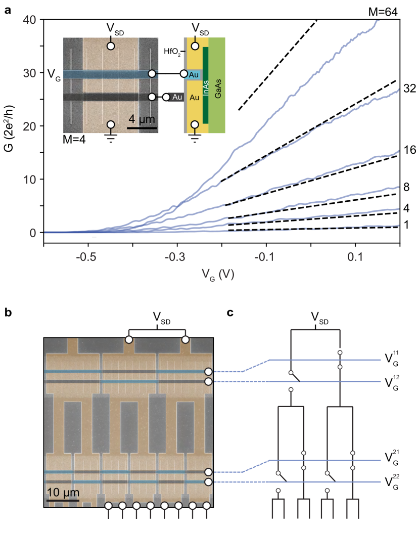
The Fig. 2a inset shows a scanning electron microscope (SEM) micrograph of a typical device along with a schematic cross section. The device includes SAG NWs connected in parallel by Ti/Au ohmic contacts and a gated segment (see Methods for fabrication details). Two gates are seen: one which acts on the exposed InAs NWs (blue), thereby controlling the conductivity, and one which is screened by the metal contact, and thus has no effect on the underlying NW (grey). This gate is, however, important for the MUX operation as discussed below. Figure 2a shows the conductance, , as a function of gate voltage, , measured at a temperature of mK for 6 different devices with varying numbers of NWs, after subtraction of a constant series resistance (see Methods). The devices act as normally-on, -type FETs with identical threshold voltages and the dashed lines show a common fit to the relation with fixed parameters and . Except for where is somewhat lower than expected, is proportional to as expected for equally contributing NWs and the linear scaling with is typical for NW FETs. The deviation for may be due to a high sensitivity to the estimate of when the device resistance is low (Methods). Importantly, Fig. 2a shows that SAG devices manufactured in parallel exhibit consistent vs , with reproducible, -independent , enabling the use of large- FETs as building blocks in LSI SAG circuits.
SAG multiplexers
We utilize the reproducibility to operate the circuit shown in Fig. 2b. SAG FETs are connected in a hierarchical MUX structure, with each level consisting of devices fabricated on different rows of the SAG NW array in Fig. 1d. Each gate spans the respective row, and the positions of the gated segment alternate such that for each NW FET, one gate (blue) tunes the carrier density of the NWs while the other is screened (grey). Input signals are thus directed through the MUX as illustrated in the schematic in Fig. 2c. With this design, each additional level doubles the number of outputs such that a level MUX has outputs and requires gates for operation.
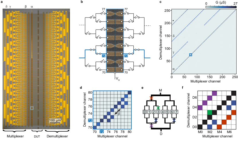
Figure 3a shows an optical micrographs of an 8-level MUX circuit connected back-to-back to a corresponding 8-level d-MUX. The circuit has a footprint of and incorporates 8192 individual SAG NWs in the form of 1996 interconnected FETs. Combining the 32 gate lines with two separate source-drain pairs enables individual addressing of any of 512 devices under test (DUT) located in the gap between the MUX/d-MUX units. Where the DUT themselves consist of FETs with a single common gate, 37 control lines thereby enable experiments on 512 devices. In our case, the DUT in Fig. 3a consist of SAG devices with different functionalities and properties. For example, the SEM micrograph in Fig. 3b shows DUT devices #70 - 77. Odd-numbered devices #71,73,75,77 are SAG NWFETs with a contact separation of 100 nm and a common top gate. The even-numbered channels consist of continuous metal paths covering the NW. These allow confirmation of the MUX/d-MUX function irrespective of the DUT performance and also provide for reference measurements the MUX and d-MUX series resistance.
Before discussing DUT properties, we analyze the functionality of the MUX/d-MUX circuit. Figure 3c shows the conductance of the circuit for each of the 65536 combinations of the first 256 MUX and d-MUX channels. The measurement was performed with positive voltage on the DUT gates, which were therefore all conducting. Indeed, high conductance is observed along the main diagonal, (), which corresponds to both MUX and d-MUX addressing the same DUT channel. This confirms that none of the 1996 SAG NWFETs of the MUX/d-MUX pair fail conduct which would lead to regions of no conductance along the diagonal. In the case of negative on the DUT level, every second pixel of the diagonal has (Supplementary Section S5). In the ideal case, the diagonal would be the only non-zero values of the conductance matrix. However, finite off-diagonal conductivity also appears following a repeating pattern every 4, 64, and 128 channels in Fig. 3c and d (). Since the FETs are conducting at , finite current at these combinations of MUX and d-MUX channels corresponds to rows of NW FETs failing to respond to the gates. This was likely due to a break in gate-lines or a failing bond wire which can occur for large, complex circuits. Figure 3e and f schematically illustrates the correlation between the patterns of the matrix and FETs failing to pinch off turn off at various positions in the circuit. For example, a non-responsive gate, on the second d-MUX level from the DUT layer (blue cross in Fig. 3e) would allow transport for (MUX,d-MUX) combinations (2,0), (3,1), (6,4), and (7,5) as indicated by blue in Fig. 3f. Comparing to the measurement in Fig. 3c and Fig. 3d the periodically repeating off-diagonal pattern can be assigned to failures of one of the gates in the MUX levels marked with the corresponding labels in Fig. 3a. The additional feature appearing at d-MUX channel 192 () results from the combination of faulty FETs at channels 64 and 128 (Supplementary Section S7 and S8 provides a further analysis of the faults of the circuit).
Importantly, the MUX/d-MUX configuration allows for identifying and in most cases self-corrects for malfunctioning elements of the SAG circuit; the double redundancy makes the measurement tolerant towards non-symmetrical errors, as, e.g., a non-functioning gate on the MUX side will be intrinsically corrected for by the function of the corresponding d-MUX gate. While errors appearing symmetrically in the MUX and d-MUX side of the circuit cannot be corrected for, they can be identified in the conductance matrix and the corresponding DUT can be excluded from experiments/analysis. This is schematically illustrated in Fig. 3e and f: if the MUX/d-MUX FETs fail to pinch-off at the symmetric red/purple positions, addressing levels 0,1,2,3 would also mix signals from levels 4,5,6,7, respectively. Such a situation is readily identified by the symmetric off-diagonal non vanishing elements in the conductance matrix (purple and red in Fig. 3f). We note that FETs failing to pinch-off would pass unnoticed in single-ended MUX layoutssmith:2020 where DUT share a common ground. The opposite case, where MUX FETs fail to open would result in periodic non-conductive elements in the diagonal of the matrix. Other examples of MUX/d-MUX circuits are discussed in Supplementary Section S6, showing that even with the amount of failures typical for research-level devices, the self-correcting nature of MUX/d-MUX configuration generally protects against a reduction in the available number of DUT.
As a final comment on MUX operation, we note that bandwidth is a key issue for control electronics. In our experiments, bandwidth was limited by the cryogenic setup, being optimized for low electron temperature, including low-pass filtering of each line. The MUX operation was uninhibited up to these frequencies (Supplementary Section S9), and we expect much higher bandwidth to be possible similar to other InAs NW electronics operating at GHztomioka:2012 ; johansson:2014 ; egard:2010 .
Multiplexing of Quantum dot arrays
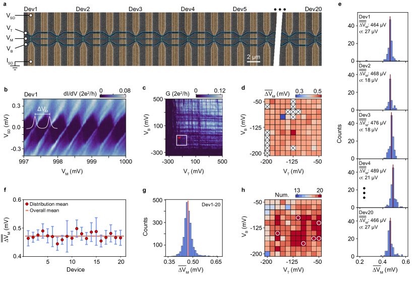
Eliminating the device-count road block by the MUX/d-MUX circuit enables fundamentally new experimental approaches in quantum electronics. For example, adding statistical significance to the characterization and optimization of device performance and material properties is crucial for efforts towards up-scaling of quantum circuits. As an example, we demonstrate here the use of the circuit for establishing the statistical reproducibility within large ensembles of lithographically identical devices. An array of 50 lithographically identical SAG quantum dot devices were embedded in the DUT layer as shown in Fig. 4a. Potentials (, , ) applied to three shared gates (top, middle, bottom) simultaneously tune the electrostatics of all 50 devices. This cross-bar approach is an important strategy for limiting the gate-count in up-scaling of QD arrays, however, successful operation requires significant reproducible between devicesli2018crossbar ; Borsoi:2022 . Here we benchmark the consistency in the SAG NW QD array by comparing the statistical distributions of QD parameters among devices labeled Dev1-Dev20. First, however, since InAs SAG QDs have thus far not been demonstrated, we establish the characteristics of a single device (Dev1).
Figure 4c shows vs. and for fixed . Pinch-off is at for both and , and horizontal/vertical structures are attributed to resonances below each gate modulating the transmissiondoh:2005 . With both gates near pinch-off, electrons are ideally confined to a NW segment below the middle gate, thus defining a QD. Indeed, fixing and at the position of the red dot in Fig. 4c, diamond shaped regions of low conductance associated with Coulomb blockade (CB) are observed in the map of the differential conductance, , vs. source bias and , as shown in Fig. 4b. The -height of the diamonds provides an estimate of the QD addition energy, being the sum of the electrostatic charging energy and the single-particle level spacing . As discussed in Supplementary Section S10 the QDs have and from Fig. 4b we estimate . The capacitance between the QD and the middle plunger gate is estimated as where is the average value CB peaks spacings in the range of Fig. 4b. This value agrees with the result () of simple capacitance estimate based on the gate layout (Supplementary Section S10) and thus support that in this particular gate-configuration, the QD confinement is defined by gates as intended.
To investigate the sensitivity to the tuning, was measured at equally spaced points, spanning the white square in Fig. 4c. CB peaks were identified at 108 of the 121 gate-tunings and Fig. 4d shows the corresponding map of . No systematic trend is observed and the distribution of shown in Fig. 4e (top), is symmetric with a mean and standard deviation , again consistent with a QD defined between the top and bottom gates.
The choice of range for the cross-bar gate-tunings in Fig. 4b,d was based on the gate characterization specific for Dev1 (Fig. 4c). We now use the MUX circuit to gather statics for the different devices in order to probe the consistency across the array while keeping these same tuning parameters. Values of were extracted from traces measured for all devices and all gate-points. All devices were operational and exhibited coulomb blockade and from the resulting 2420 gate-traces, 17924 CB peaks were identified and fitted. Examples of measured data and peak analysis are presented in Supplementary Section S12 and S13. The distributions of for all devices are included in Supplementary Section S14 and examples for Dev2-5 are shown in Fig. 4e. A comparison of the distributions and their mean values, , among the devices of the array, is shown in Fig. 4f. Except for Dev7, the distribution means fall within one of the overall common mean. The spread between devices could be affected by structural variations between nanowires due to SAG processing or to variation in post growth device processing. The spread within each devices could be related to changes in the effective confinement potential with gate tunings and may be different between devices due to random impurity in the vicinity of the devices.
Finally, Fig. 4g shows the joint distribution of all and Fig. 4h illustrates the number of devices displaying CB for all measured combinations of , . In 27 out of the 121 point in cross-bar gate space, all 20 devices simultaneously exhibiting CB. The circles mark the 7 tunings where all devices fulfill the stricter criterion of showing CB and having within of the joint mean peak spacing. Figure 4f-h constitute a key result of the current study, establishing both a level of device to device reproducibility supporting the potential of SAG for as a scalable platform for quantum electronics. Further, the statistical bench-marking of the QD devices explicitly demonstrates a key example of the new possibilities enabled by the integration of MUX/d-MUX circuits.
Conclusions and Outlook
In conclusion, we successfully fabricated and operated cryogenic multiplexers/de-muliplexer circuits based on InAs NWs grown bottom-up by selective area growth. The circuit removes the limitations on device count in conventional cryogenic electronics thus enabling new experimental strategies such as searches through large ensembles of devices for rare or exotic phenomena, establishing the correlation between device performance and materials properties or device geometry, and allows establishing the statistical reproducibility among devices - a prerequisite for further scaling quantum of circuits. This capacity was demonstrated by statistically characterizing an ensemble of SAG quantum dots. In general, the methods developed here enable optimization of quantum materials and devices based on automated acquisition of statistically significant datasets rather than proof-of-principle examples. This direction will be empowered by the ongoing developments of advanced data evaluationlesage:2015 and machine learningzwolak:2020 ; moon:2020 ; nguyen:2021 for unsupervised and optimized acquisition and tuning of large ensembles of quantum devices with many tuning parameterslennon:2019 ; darulova:2020 ; chatterjee:2022 . The circuit may be expanded further by replacing the single lines in the current design by a multi-channel busward:2013 to enable, e.g., integration of charge sensors, multi-terminal devices, complex gate-architectures, and/or the operating the MUX as a multi-channel DACpuddy:2015 .
Methods
For SAG fabrication and synthesis, a \ceSiO2 mask layer was first deposited on epi-ready GaAs \hkl(311)A substrates by plasma enhanced chemical vapour deposition. rectangular openings were defined in the oxide along the \hkl[0-11] direction by e-beam lithography (EBL) and dry etching. The openings were arranged in arrays with a pitch of and along the \hkl[0-11] and \hkl[-233], respectively (Fig. 1d). GaAs(Sb)/InAs double layer NWs were selectively grown in the openings where the GaAs(Sb) buffer was introduced to improve the crystal surface for the subsequent InAs transport channelKrizek2018Sep . Synthesis details and structural analysis are provided in Supplementary Sections S1 and S2. For device fabrication, Ti/Au ohmic contacts to the SAG NWs were defined on the growth substrate by standard EBL, metal evaporation, and liftoff. Subsequently, a \ceHfO2 gate dielectric was deposited by atomic layer deposition and top-gates were defined by electron beam lithography, metal evaporation, and liftoff. The QD devices in Fig. 4 have a contact separation of 900 nm, top/middle/bottom cross-bar gates are 300/200/300 nm wide and have a 150 nm spacing. Electrical measurements were carried out in a dilution refrigerator with a base temperature of . The conductance, , where is the drain current generated by source voltage , was measured as a function of the gate potential, , using standard lock-in techniques. The series resistance for data presented in Fig. 2 was estimated by fitting the traces with the standard expressiongul2015towards where is the gate length, is gate capacitance simulated as described in Supplementary Section S3 and S4, and is the electron mobility. When sweeping in the QD measurements, the barrier gates were compensated for a slight capacitive cross coupling (Supplementary Section S10).
Data availability
Full data sets for all figures, STEM micrographs, transport data, electronic logbooks and other data that support the findings of this study are available online at
https://sid.erda.dk/
Acknowledgements
This research was supported by research grants from Villum Fonden (00013157) and the European Research Council (866158). ICN2 acknowledges funding from Generalitat de Catalunya 2021SGR00457. The authors thank support from “ERDF A way of making Europe”, by the “European Union”. ICN2 is supported by the Severo Ochoa program from Spanish MCIN / AEI (Grant No.: CEX2021-001214-S) and is funded by the CERCA Programme / Generalitat de Catalunya. Authors acknowledge the use of instrumentation as well as the technical advice provided by the National Facility ELECMI ICTS, node ”Laboratorio de Microscopías Avanzadas” at University of Zaragoza. We acknowledge support from CSIC Interdisciplinary Thematic Platform (PTI+) on Quantum Technologies (PTI-QTEP+).
Competing interests
The authors declare no competing financial interests
Supporting Information
Supporting information contains extended information on sample preparation and MBE growth, NW structure investigation via GPA, extended transport datasets for Fig. 4b, details of the fitting procedures employed for Fig. 4c and d, as well as a more in-depth description of the MUX/d-MUX circuit benchmarking, measurement bandwidth, and switching speed.
References
- (1) Mourik, V. et al. Signatures of Majorana Fermions in Hybrid Superconductor-Semiconductor Nanowire Devices. Science 336, 1003–1007 (2012).
- (2) Hu, Y. et al. A Ge/Si Heterostructure Nanowire-Based Double Quantum Dot with Integrated Charge Sensor. Nature Nanotechnology 2, 622–625 (2007).
- (3) Hofstetter, L., Csonka, S., Nygård, J. & Schönenberger, C. Cooper Pair Splitter Realized in a Two-Quantum-Dot Y-junction. Nature 461, 960–963 (2009).
- (4) Fasth, C., Fuhrer, A., Björk, M. T. & Samuelson, L. Tunable Double Quantum Dots in InAs Nanowires Defined by Local Gate Electrodes. Nano letters 5, 1487–1490 (2005).
- (5) Doh, Y.-J. et al. Tunable Supercurrent Through Semiconductor Nanowires. Science 309, 272–275 (2005).
- (6) Xiang, J., Vidan, A., Tinkham, M., Westervelt, R. M. & Lieber, C. M. Ge/Si Nanowire Mesoscopic Josephson Junctions. Nature Nanotechnology 1, 208–213 (2006).
- (7) Larsen, T. W. et al. Semiconductor-Nanowire-Based Superconducting Qubit. Phys. Rev. Lett. 115, 127001 (2015).
- (8) Krogstrup, P. et al. Epitaxy of Semiconductor–Superconductor Nanowires. Nature Materials 14, 400–406 (2015).
- (9) Hays, M. et al. Direct Microwave Measurement of Andreev-Bound-State Dynamics in a Semiconductor-Nanowire Josephson Junction. Phys. Rev. Lett. 121, 047001 (2018).
- (10) Svensson, J., Dey, A. W., Jacobsson, D. & Wernersson, L.-E. III–V Nanowire Complementary Metal–Oxide Semiconductor Transistors Monolithically Integrated on Si. Nano Letters 15, 7898–7904 (2015).
- (11) Tomioka, K., Yoshimura, M. & Fukui, T. A III–V Nanowire Channel on Silicon for High-Performance Vertical Transistors. Nature 488, 189–192 (2012).
- (12) Freer, E. M., Grachev, O., Duan, X., Martin, S. & Stumbo, D. P. High-Yield Self-Limiting Single-Nanowire Assembly with Dielectrophoresis. Nature Nanotechnology 5, 525–530 (2010).
- (13) Yao, J., Yan, H. & Lieber, C. M. A Nanoscale Combing Technique for the Large-Scale Assembly of Highly Aligned Nanowires. Nature Nanotechnology 8, 329–335 (2013).
- (14) Li, M. et al. Bottom-up Assembly of Large-Area Nanowire Resonator Arrays. Nature Nanotechnology 3, 88–92 (2008).
- (15) Wang, N. et al. Shape Engineering of InP Nanostructures by Selective Area Epitaxy. ACS Nano 13, 7261–7269 (2019).
- (16) Op het Veld, R. L. et al. In-Plane Selective Area InSb–Al Nanowire Quantum Networks. Communications Physics 3, 1–7 (2020).
- (17) Raya, A. M. et al. GaAs Nanoscale Membranes: Prospects for Seamless Integration of III–Vs on Silicon. Nanoscale 12, 815–824 (2020).
- (18) Bollani, M. et al. Selective Area Epitaxy of GaAs/Ge/Si Nanomembranes: A Morphological Study. Crystals 10, 57 (2020).
- (19) Aseev, P. et al. Selectivity Map for Molecular Beam Epitaxy of Advanced III–V Quantum Nanowire Networks. Nano Letters 19, 218–227 (2019).
- (20) Krizek, F. et al. Field Effect Enhancement in Buffered Quantum Nanowire Networks. Phys. Rev. Mater. 2, 093401 (2018).
- (21) Beznasyuk, D. V. et al. Doubling the Mobility of InAs/InGaAs Selective Area Grown Nanowires. Phys. Rev. Materials 6, 034602 (2022).
- (22) Friedl, M. et al. Template-Assisted Scalable Nanowire Networks. Nano Letters 18, 2666–2671 (2018).
- (23) Lee, J. S. et al. Selective-Area Chemical Beam Epitaxy of In-Plane InAs One-Dimensional Channels Grown on InP(001), InP(111)B, and InP(011) surfaces. Phys. Rev. Mater. 3, 084606 (2019).
- (24) Vaitiekėnas, S. et al. Selective-Area-Grown Semiconductor-Superconductor Hybrids: A Basis for Topological Networks. Phys. Rev. Lett. 121, 147701 (2018).
- (25) Hertel, A. et al. Gate-Tunable Transmon Using Selective-Area-Grown Superconductor-Semiconductor Hybrid Structures on Silicon. Phys. Rev. Appl. 18, 034042 (2022).
- (26) Ten Kate, S. C. et al. Small Charging Energies and g -Factor Anisotropy in PbTe Quantum Dots. Nano Letters 22, 7049–7056 (2022).
- (27) Schmid, H. et al. Template-assisted selective epitaxy of III–V nanoscale devices for co-planar heterogeneous integration with Si. Appl. Phys. Lett. 106, 233101 (2015).
- (28) Gooth, J. et al. Ballistic One-Dimensional InAs Nanowire Cross-Junction Interconnects. Nano Letters 17, 2596–2602 (2017).
- (29) Pauka, S. et al. Characterizing Quantum Devices at Scale with Custom Cryo-CMOS. Phys. Rev. Applied 13, 054072 (2020).
- (30) Paquelet Wuetz, B. et al. Multiplexed Quantum Transport Using Commercial Off-the-Shelf CMOS at Sub-Kelvin Temperatures. Quantum Information 6, 1–8 (2020).
- (31) Smith, L. W. et al. Statistical Study of Conductance Properties in One-Dimensional Quantum Wires Focusing on the 0.7 Anomaly. Phys. Rev. B 90, 045426 (2014).
- (32) Smith, L. W. et al. High-Throughput Electrical Characterization of Nanomaterials from Room to Cryogenic Temperatures. ACS Nano 14, 15293–15305 (2020).
- (33) Loss, D. & DiVincenzo, D. P. Quantum Computation With Quantum Dots. Phys. Rev. A 57, 120 (1998).
- (34) Tomioka, K., Motohisa, J. & Fukui, T. Rational Synthesis of Atomically Thin Quantum Structures in Nanowires Based on Nucleation Processes. Scientific Reports 10, 1–9 (2020).
- (35) Vandersypen, L. M. & Eriksson, M. A. Qauntim Computing With Semiconductor Spins. Physics Today 72, 8–38 (2019).
- (36) Li, R. et al. A Crossbar Network for Silicon Quantum Dot Qubits. Science Advances 4, eaar3960 (2018).
- (37) Borsoi, F. et al. Shared control of a 16 semiconductor quantum dot crossbar array (2022). URL https://arxiv.org/abs/2209.06609.
- (38) Johansson, S., Memisevic, E., Wernersson, L.-E. & Lind, E. High-Frequency Gate-All-Around Vertical InAs Nanowire MOSFETs on Si Substrates. IEEE Electron Device Lett. 35, 518–520 (2014).
- (39) Egard, M. et al. Vertical InAs Nanowire Wrap Gate Transistors with GHz and GHz. Nano Letters 10, 809–812 (2010).
- (40) Lesage, A. A. J. et al. Assisted extraction of the energy level spacings and lever arms in direct current bias measurements of one-dimensional quantum wires, using an image recognition routine. Journal of Applied Physics 117, 015704 (2015).
- (41) Zwolak, J. P. et al. Autotuning of Double-Dot Devices In Situ with Machine Learning. Phys. Rev. Appl. 13, 034075 (2020).
- (42) Moon, H. et al. Machine Learning Enables Completely Automatic Tuning of a Quantum Device Faster Than Human Experts. Nature Communications 11, 4161 (2020).
- (43) Nguyen, V. et al. Deep Reinforcement Learning for Efficient Measurement of Quantum Devices. Quantum Information 7, 1–9 (2021).
- (44) Lennon, D. T. et al. Efficiently Measuring a Quantum Device Using Machine Learning. Quantum Information 5, 1–8 (2019).
- (45) Darulová, J. et al. Autonomous Tuning and Charge-State Detection of Gate-Defined Quantum Dots. Phys. Rev. Appl. 13, 054005 (2020).
- (46) Chatterjee, A. et al. Autonomous Estimation of High-Dimensional Coulomb Diamonds from Sparse Measurements. Phys. Rev. Applied 18, 064040 (2022).
- (47) Ward, D. R., Savage, D. E., Lagally, M. G., Coppersmith, S. N. & Eriksson, M. A. Integration of On-Chip Field-Effect Transistor Switches with Dopantless Si/SiGe Quantum Dots for High-Throughput Testing. Applied Physics Letters 102, 213107 (2013).
- (48) Puddy, R. K. et al. Multiplexed Charge-Locking Device for Large Arrays of Quantum Devices. Applied Physics Letters 107, 143501 (2015).
- (49) Gül, Ö. et al. Towards High Mobility InSb Nanowire Devices. Nanotechnology 26, 215202 (2015).