figurec
Analog Feedback-Controlled Memristor programming Circuit for analog Content Addressable Memory
Abstract
Recent breakthroughs in associative memories suggest that silicon memories are coming closer to human memories, especially for memristive Content Addressable Memories (CAMs) which are capable to read and write in analog values. However, the Program-Verify algorithm, the state-of-the-art memristor programming algorithm, requires frequent switching between verifying and programming memristor conductance, which brings many defects such as high dynamic power and long programming time. Here, we propose an analog feedback-controlled memristor programming circuit that makes use of a novel look-up table-based (LUT-based) programming algorithm. With the proposed algorithm, the programming and the verification of a memristor can be performed in a single-direction sequential process. Besides, we also integrated a single proposed programming circuit with eight analog CAM (aCAM) cells to build an aCAM array. We present SPICE simulations on TSMC 28nm process. The theoretical analysis shows that 1. A memristor conductance within an aCAM cell can be converted to an output boundary voltage in aCAM searching operations and 2. An output boundary voltage in aCAM searching operations can be converted to a programming data line voltage in aCAM programming operations. The simulation results of the proposed programming circuit prove the theoretical analysis and thus verify the feasibility to program memristors without frequently switching between verifying and programming the conductance. Besides, the simulation results of the proposed aCAM array show that the proposed programming circuit can be integrated into a large array architecture.
1 Introduction
Associative memories are inherent in human brains. Through association, the features of a new object can be matched with another object with similar features existing in our memory, and thus this new object can be simply remembered. In general, associative memories allow us to link uncorrelated information and hence are an essential feature of our intelligence[1].
Inspired by the biological and psychological concept of associative memories, different hardware approaches to such systems have been realized recently. W. A. Borders et al. proposed an analog spin-orbit torque device for ANN-based associative memory operation [2]. Pavlov associative memory has been implemented in circuits by different groups [3][4]. In recent years, memristive CAMs have been regarded as critical hardware in a wide range of associative memory applications: Li et al. designed the first aCAM which allows for searching in analog values[5]; G. Pedretti et al. used aCAM to introduce a new compute concept for tree-based learning techniques (e.g., decision trees and random forests)[6]; C. E. Graves et al. proposed an 8612 memristor ternary CAM (TCAM) array for pattern matching[7]; Furthermore, differential CAM (dCAM) is also a viable option for associative memory architectures[8].
However, good memristor programming techniques are necessary for both aCAM and dCAM arrays to achieve an accurate and fast writing process without losing high memory density. Here we present a novel LUT-based programming algorithm for memristors that utilizes an analog feedback control mechanism to enable highly precise programming of a 10T2M aCAM cell[9]. We will also show the possibility to integrate the proposed programming circuit in a 10T2M aCAM array. With the proposed programming circuit, the aCAM array can properly set, reset, or read the conductance of the memristor within a single cell, and hence provide individual addressing. Besides, our results prove that the memristor programming algorithm is possible to replace the traditional Program-Verify algorithm for memristor programming in analog CAMs.
2 analog feedback-controlled memristor programming circuit
2.1 10T2M aCAM Cell
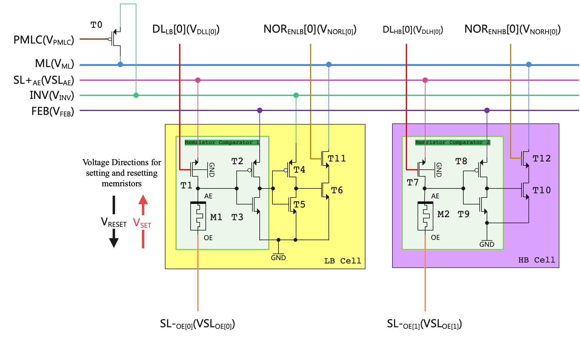
To enhance the programming capability of the 10T2M cell proposed in [6] and [9] using our proposed algorithm, we implemented a series of modifications as shown in Fig. 1, including:
-
1.
The original aCAM design utilizes 1T1R structures with memristors connected to the OE electrode, and the CAM search is performed in the reset direction. Our design features an interchanged position between the memristor and transistor T1, with the Memristor AE now connected to the transistor. This configuration results in improved performance during set operations by eliminating the body effect, when applying a set voltage. [10]
- 2.
-
3.
T11 and T12 are added in the LB cell and the HB cell respectively. These transistors add a "don’t care" option in CAM search to each cell. They also ensure in during a search operation that the CAM cell is disconnected from the ML. These transistors are used to disconnect the CAM cell from the match line (ML) during a search operation, which prevents false matches caused by the internal capacitance charging at the beginning of each search pulse. In the program mode, when these transistors are off, any input at the data line (DL) won’t affect the voltage at the match line (ML), which enables the use of the ML voltage in the programming circuit to write to an individual memristor.
2.2 The LUT-based memristor programming algorithm
Traditionally, the Program-Verify Algorithm is the state-of-the-art algorithm used to program memristors[11][12]. However, while utilizing this algorithm, frequent switching between searching and programming is necessary, which leads to high programming accuracy but also results in high dynamic power consumption and lower programming speed. Besides, it requires stricter timing in peripheral circuits. Here, we present a LUT-based algorithm that can perform programming and verification simultaneously.
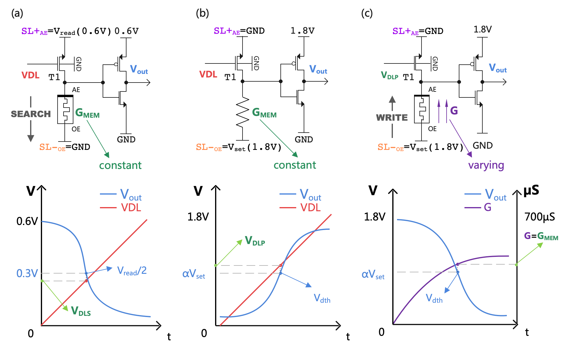
The demonstration of the proposed algorithm first starts with the analysis of the circuit in search mode shown in Fig. 2 (a). This circuit is called the "Memristor Comparator", which is present in the LB cell and the HB cell of the 10T2M aCAM cell. In circuit (a), the memristor is supplied with a low ( ), which means the conductance of the memristor remains is close to constant. To simplify the calculations, the inverter in this circuit is assumed as ideal (). First a linear voltage sweep is applied as transient simulation ranging from at the input of the aCAM cell. By increase of the output voltage will drop from a high voltage to a lower voltage, since the intermediate voltage between transistor and memristor will rise. If the resistor and the transistor reach the same conductance, ideally will drop from to 0. During the simulation, the value which leads drop or rise is the desired programming value since it represents the boundary voltage to which the input is compared. For schematic (a), this value is named . If the transistor body effects are neglected, the drain current of the transistor at the point can be calculated as below:
| (1) |
Then the relationship between and the memristor conductance () can be deducted from the above equations:
| (2) |
Equation. 2 demonstrates that the relation of the conductance of the memristor within the memristor comparator from Fig. 1 to the resulting boundary votlage is linear. This circumstance can be utilized to simplify programming by allowing for the programming of a boundary voltage instead of a conductance within the memristor comparator. Conclusion )
Secondly, schematic (b) is compared with schematic (a) to analyze the relationship between and , since in programming mode, when sweeping the a certain specific boundary voltage can be observed. Circuit (b) is a CMOS circuit that substitutes the memristor in (a) with a resistor of the same conductance to assume it as a constant device. and , which means that a set voltage is applied and the transistor T1 in circuit (b) can reach saturation region. Now a simulation is performed by inserting a linear voltage sweep ( ) at the transistor gate. With sweep of , the output voltage will rise from a low voltage to a high voltage. After this the is saved which makes the rise to a certain value (), and name this value as the boundary voltage in programming mode . Assuming that the inverter in this circuit is ideal () and neglecting the transistor body effects, then the boundary voltage in programming mode can be calculated as below:
| (3) |
The equation above demonstrates the relationship between and . This allows a specific boundary voltage to be programmed in set mode by retrieving the related boundary voltage in read mode, , from a lookup table.(Conclusion )
The schematic from Fig. 1 (c) the 1T1R is again realized with a memristor. In this case, the input voltage is not swept; instead, a constant DC voltage, , is applied to the T1 gate. As is set to , the memristor comparator operates in writing mode. Now start a simulation for both circuit (b) and circuit (c). In circuit (b), will sweep and the output voltage will start to rise as discussed before. In circuit (c), the memristor conductance will increase because the memristor will be programmed under a high and . Thus, the continuously rising conductance will pull down the output voltage. When the output voltage of circuit (c) is decreased to , it’s obvious that at this moment circuit (c) has the same working points as circuit (b) when the output voltage of (b) rises also to . Hence, when reaches in circuit (c), the memristor in this circuit has a conductance of , which is the same as the conductance of the resistor in circuit (b).
The above deductions prove that when the output voltages of these two circuits are the same, the memristor conductance in circuit (c) equals to the resistor conductance in circuit (b), and thus at this moment Equation. 4 originally calculated for circuit (b) is also valid for circuit (c) (Conclusion ).
Based on Conclusion , and , a deduction can made be that programming the memristor conductance within circuit (a) can be switched to using a as input in circuit (c), and wait until the output voltage drops to . (Conclusion ) It’s obvious that circuit (a) and circuit (c) can represent the working status of the search mode and the program mode of aCAM cells. Consequently, Conclusion provides an algorithm to program the memristors. Using this algorithm the memristor conductance can be calculated based on Equation. 2 and Equation. 4:
| (5) |
Equation. 5 demonstrates that for the same memristor comparator circuit, a LUT between programming voltage () and the programmed memristor conductance () can be built. An example LUT is shown in Table.1. In this table is set at . The equations above are calculated under the assumption that the transistor operates with a common long-channel quadratic function in the saturation region. In reality, the equation between and depends on the transistor technology. In this paper, the simulations use TSMC 28nm technology. The transistor follows a linear function in the saturation region, and thus the programmed memristor conductance shows a linear relationship with the programming voltage.
2.3 Programming circuit
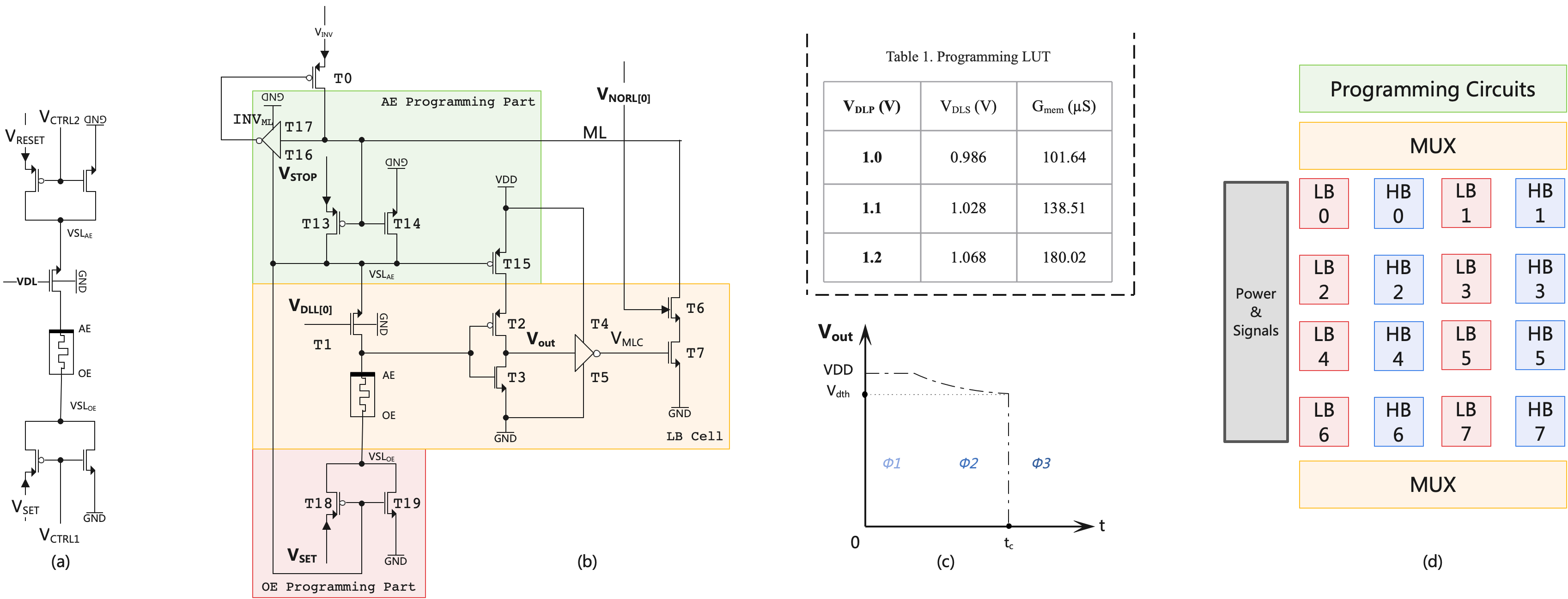
To achieve the LUT-based memristor programming algorithm proposed above, the programming circuits for 10T2M LB cell is designed in Fig. 3b. For all descriptions below, please refer to this diagram. Because the LB programming circuit and the HB programming circuit have similar circuit behaviors, only the programming operations in the LB cell will be demonstrated in this subsection. To set the memristor, the programming process can be roughly divided into 3 phases:
In the first phase (1:Prepare Phase), is charged to a high voltage level (HIGH), and must remain at a low voltage level (LOW). In this case, the ML voltage is locked at HIGH. This will make tend to connect the GND and tend to connect . Now the whole circuit is ready for setting the memristor.
At the beginning of 2 (Set Phase), , and should be charged with corresponding high voltage. also needs to receive the programming voltage. After these signals get stable the conductance of the memristor will gradually increase, making descend slowly until reaches its threshold (), as shown in Fig. 3c.
After reaches its threshold , then the circuit comes to 3 (Stop Phase). When tends to be pulled down, on the other hand, will continuously rise to HIGH, which will pull down . In the circuit, the trend of ML pull-down will be strengthened by the ML inverter () and the ML PMOS (T0). At the same time, because ML controls the set-reset peripheral circuit, a lower will lead to a higher and a lower , which will switch the set-reset peripheral circuit tile to the resetting state. Besides, a rising will reduce the source voltage of T15 and to a further extent reduce . With the above positive feedback, drops to LOW at an extremely fast speed.
To reset the memristor, a high voltage needs to apply at , then very high voltage needs to apply at and . After signals are set up, the memristor can be reset to the lowest possible conductance.
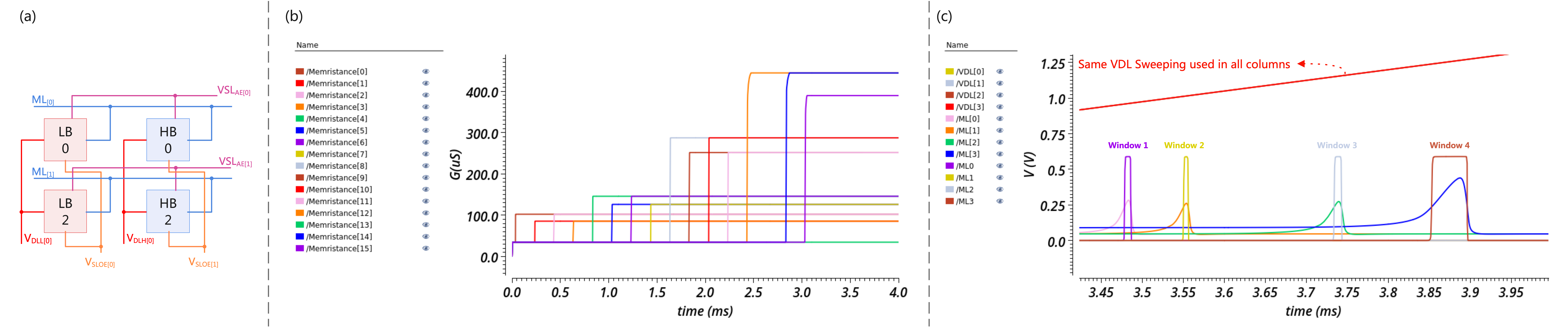
2.4 aCAM array design
For convenience, if the aCAM cell (Fig. 2) is drawn with LB and HB blocks, a simplified architecture of the proposed 8-Cell aCAM array design is shown in Fig. 3d. The array has four working modes: Writing Mode (WR), Resetting Mode (RST), Sweeping Mode (SW), and Verify Mode (VR). Besides, the array has 2 states: the programming state and the searching state. In the programming state, the array is programming the memristor in LB or HB cells to different conductance levels, followed by some checking and verification work. In the searching state, the parallel is input to the array and the array will check if there is a match in a row.
The functions of each working mode are listed below:
-
1.
In the WR, the conductance of the memristor in an LB cell or an HB cell is set to the desired value.
-
2.
In the RST, the memristor is reset to the lowest possible conductance.
-
3.
In the SW, a voltage sweep between to is used at . This mode is used to check whether the aCAM cell works normally.
-
4.
In the VR, is applied at . This mode is used to precisely measure the memristor conductance.
3 Simulation Results
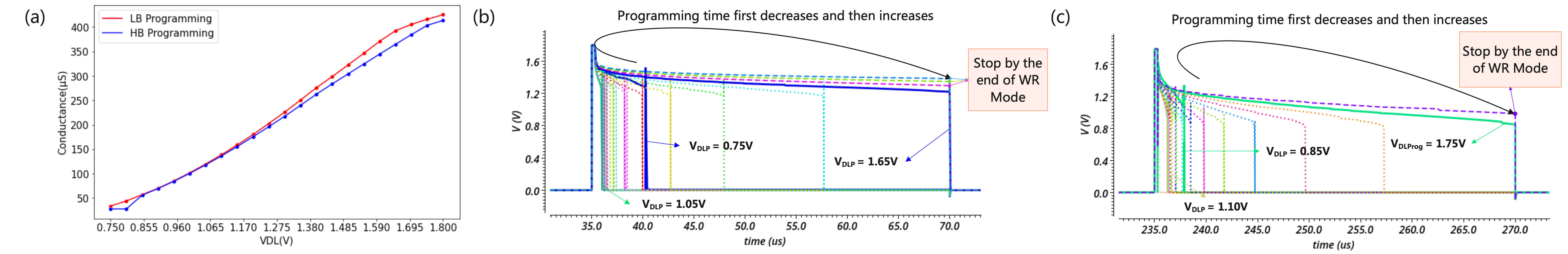
An attractive feature of the proposed analog feedback-controlled programming circuits is the possibility to program the memristor conductance only using the data line voltage as a input parameter. To test whether the proposed memristor programming circuits and the aCAM array can achieve the programming functions, simulations for both single-cell programming and array programming have been performed. In the single-cell programming, the results Fig. 5a shows that the programmed conductance shows a linear relationship within a certain range of programmable , which also corresponds to the memristor comparator’s dynamic range. Fig. 5b and Fig. 5c show that the programming process under high programming will be stopped earlier by the end of the WR Mode.
Fig. 4c shows the memristor conductance changes of all 8 aCAM cells. Because before setting an LB or HB cell the memristor in this cell is reset to the lowest conductance, the figure proves that setting or resetting a specific cell won’t affect other cells. Figure. 4d illustrates the function of aCAM. In the Programming State, aCAM cells in rows are programmed with different matching ranges (windows). Then in the Searching State, when a sweeping is used as input, it’s clear to see the shapes of these windows.
4 Conclusion
In this article, we implement an analog feedback-controlled memristor programming circuit, which leverages the natural relationship between memristor conductance and the programming data line boundary voltage in memristor CAMs. The simulation results show that the proposed programming circuits meet the expected transient response and could achieve the LUT-based memristor programming algorithm. In addition, we manage to integrate eight 10T2M aCAM cells with a single programming circuit. The simulations prove that the proposed array architecture can achieve the functions of an aCAM array.
Despite the benefits of the proposed hardware architectures, the memristor devices still have many non-ideal characteristics, such as device to device and cycle to cycle variability, read noise and conductance drifts, which are not considered in this article. In addition, the ML parasitics of the proposed array are not fully counted in the simulations, which may affect the final results of the read/write speed and memory density. The aforementioned non-idealities will be considered and analyzed in our future work.
References
- Suzuki [2005] Wendy A Suzuki. Associative learning and the hippocampus. 2005.
- Kour and Saabne [2014] George Kour and Raid Saabne. Fast classification of handwritten on-line arabic characters. In Soft Computing and Pattern Recognition (SoCPaR), 2014 6th International Conference of, pages 312–318. IEEE, 2014.
- Wang et al. [2016] Lidan Wang, Huifang Li, Shukai Duan, Tingwen Huang, and Huamin Wang. Pavlov associative memory in a memristive neural network and its circuit implementation. Neurocomputing, 171:23–29, 2016.
- Sun et al. [2022] Chenyang Sun, Chunhua Wang, and Cong Xu. A full-function memristive pavlov associative memory circuit with inter-stimulus interval effect. Neurocomputing, 506:68–83, 2022.
- Li et al. [2020] Can Li, Catherine E Graves, Xia Sheng, Darrin Miller, Martin Foltin, Giacomo Pedretti, and John Paul Strachan. Analog content-addressable memories with memristors. Nature communications, 11(1):1638, 2020.
- Pedretti et al. [2021] Giacomo Pedretti, Catherine E Graves, Sergey Serebryakov, Ruibin Mao, Xia Sheng, Martin Foltin, Can Li, and John Paul Strachan. Tree-based machine learning performed in-memory with memristive analog cam. Nature communications, 12(1):5806, 2021.
- Graves et al. [2020] Catherine E Graves, Can Li, Xia Sheng, Darrin Miller, Jim Ignowski, Lennie Kiyama, and John Paul Strachan. In-memory computing with memristor content addressable memories for pattern matching. Advanced Materials, 32(37):2003437, 2020.
- Pedretti et al. [2022] Giacomo Pedretti, Catherine E Graves, Thomas Van Vaerenbergh, Sergey Serebryakov, Martin Foltin, Xia Sheng, Ruibin Mao, Can Li, and John Paul Strachan. Differentiable content addressable memory with memristors. Advanced Electronic Materials, 8(8):2101198, 2022.
- Bazzi et al. [2022] Jinane Bazzi, Jana Sweidan, Mohammed E Fouda, Rouwaida Kanj, and Ahmed M Eltawil. Efficient analog cam design. arXiv preprint arXiv:2203.02500, 2022.
- Bengel et al. [2023] Christopher Bengel, Kaihua Zhang, Johannes Mohr, Tobias Ziegler, Stefan Wiefels, Rainer Waser, Dirk Wouters, and Stephan Menzel. Tailor-made synaptic dynamics based on memristive devices. Frontiers in electronic materials, 3(FZJ-2023-01070):1061269, 2023.
- Merced-Grafals et al. [2016] Emmanuelle J Merced-Grafals, Noraica Dávila, Ning Ge, R Stanley Williams, and John Paul Strachan. Repeatable, accurate, and high speed multi-level programming of memristor 1t1r arrays for power efficient analog computing applications. Nanotechnology, 27(36):365202, 2016.
- Yan et al. [2019] Bonan Yan, Bing Li, Ximing Qiao, Cheng-Xin Xue, Meng-Fan Chang, Yiran Chen, and Hai Li. Resistive memory-based in-memory computing: From device and large-scale integration system perspectives. Advanced Intelligent Systems, 1(7):1900068, 2019.