Mapping twist-tuned multi-band topology in bilayer WSe2
Abstract
Semiconductor moiré superlattices have been shown to host a wide array of interaction-driven ground states. However, twisted homobilayers have been difficult to study in the limit of large moiré wavelength, where interactions are most dominant, and despite numerous predictions of nontrivial topology in these homobilayers, experimental evidence has remained elusive. Here, we conduct local electronic compressibility measurements of twisted bilayer WSe2 at small twist angles. We demonstrate multiple topological bands which host a series of Chern insulators at zero magnetic field near a ‘magic angle’ around . Using a locally applied electric field, we induce a topological quantum phase transition at one hole per moiré unit cell. Furthermore, by measuring at a variety of local twist angles, we characterize how the interacting ground states of the underlying honeycomb superlattice depend on the size of the moiré unit cell. Our work establishes the topological phase diagram of a generalized Kane-Mele-Hubbard model in tWSe2, demonstrating a tunable platform for strongly correlated topological phases.
I Introduction
The richness of interacting condensed matter systems motivates the development of experimental platforms with tunable Hamiltonians, which can admit systematic study over a wide range of phase space bloch_quantum_2012 ; kennes_moire_2021 . Recently, moiré heterostructures have emerged as a venue to engineer flat electronic bands and realize emergent correlated states. In twisted graphene structures, interacting phases generally only form near certain ‘magic’ angles andrei_graphene_2020 ; balents_superconductivity_2020 ; cao_correlated_2018 ; cao_unconventional_2018 . In contrast, moiré transition metal dichalcogenide (TMD) heterostructures exhibit strong correlations across a wide range of twist angles (and corresponding moiré wavelengths) mak_semiconductor_2022 . Because the underlying electronic structure can often be captured by extended Hubbard models, these systems are promising for quantum simulation with effective parameters tunable by moiré wavelength, choice of TMD, and applied electromagnetic fields kennes_moire_2021 ; wu_hubbard_2018 ; zhang_moire_2020 ; tang_simulation_2020 . In practice, the ability to meaningfully adjust parameters has been limited by the experimental challenges of poor electrical contact and local disorder mak_semiconductor_2022 ; lau_reproducibility_2022 . As a result, study of correlated states in these systems to date has focused mostly on heterobilayers, where lattice mismatch provides a nearly constant moiré wavelength tang_simulation_2020 ; xu_correlated_2020 ; regan_mott_2020 ; li_continuous_2021 ; li_quantum_2021 ; li_charge-order-enhanced_2021 , or on homobilayers with large interlayer twist, where angular variations have a muted effect wang_correlated_2020 ; ghiotto_quantum_2021 ; xu_tunable_2022 . While this has resulted in the discovery of many exotic ground states, the ability to vary parameters while maintaining strong interactions relative to electronic bandwidth in a single system has remained limited.
Of particular interest is the ability to engineer tunable topological flat-band structures, in which interactions can lead to nontrivial insulating states. In graphene-based moiré superlattices, quantum anomalous Hall (QAH) insulators have been observed, but this typically requires fine-tuning of external parameters (in addition to twist angle) serlin_intrinsic_2020 ; chen_tunable_2020 ; pierce_unconventional_2021 ; polshyn_electrical_2020 ; stepanov_competing_2021 , and the topological bands do not allow a local tight-binding description andrei_graphene_2020 ; mak_semiconductor_2022 ; kane_quantum_2005 . Theoretical calculations have predicted that certain TMD moiré homobilayers realize a generalized version of the Kane-Mele model in which the lowest energy pair of bands have nonzero Chern number, and that these bands could support QAH states at odd filling due to interactions wu_topological_2019 . However, there has been disagreement in the literature about the exact parameters for which topological bands are expected devakul_magic_2021 ; pan_band_2020 . While there has been no experimental evidence of topology in TMD homobilayers to date, recent experiments in AB-stacked MoTe2/WSe2 heterobilayers were able to mimic similar physics using a large out of plane electric field to hybridize the electronic states on the two layers, and realize QAH and quantum spin hall insulating states at moiré filling factors and , respectively li_quantum_2021 ; tschirhart_intrinsic_2023 ; zhao_realization_2022 . The precise symmetry-breaking which underlies these insulating phases is a subject of ongoing experimental and theoretical studies tao_valley-coherent_2022 ; zhang_spin-textured_2021 ; xie_valley-polarized_2022 ; pan_topological_2022 ; devakul_quantum_2022 ; rademaker_spin-orbit_2022 ; dong_excitonic_2023 ; mai_interaction-driven_2023 ; mai_14_2023 .
In this work, we use scanning single electron transistor (SET) microscopy to investigate twisted bilayer WSe2 (tWSe2) at much lower relative twist angle than previously studied. By measuring at different twist angles, we map how the system depends on local moiré wavelength. In addition to widespread correlated insulating states, we find ‘magic-angle’ topology in the vicinity of . Around that twist angle, we observe a series of QAH insulators, indicating multiple moiré bands with nonzero Chern numbers. Using an applied displacement field, we drive a topological phase transition of the insulator between a QAH state and a topologically trivial layer-polarized state. Together, our results represent systematic quantum simulation of generalized Kane-Mele-Hubbard physics on a tunable real-space lattice.
II Series of Chern insulators in tWSe2
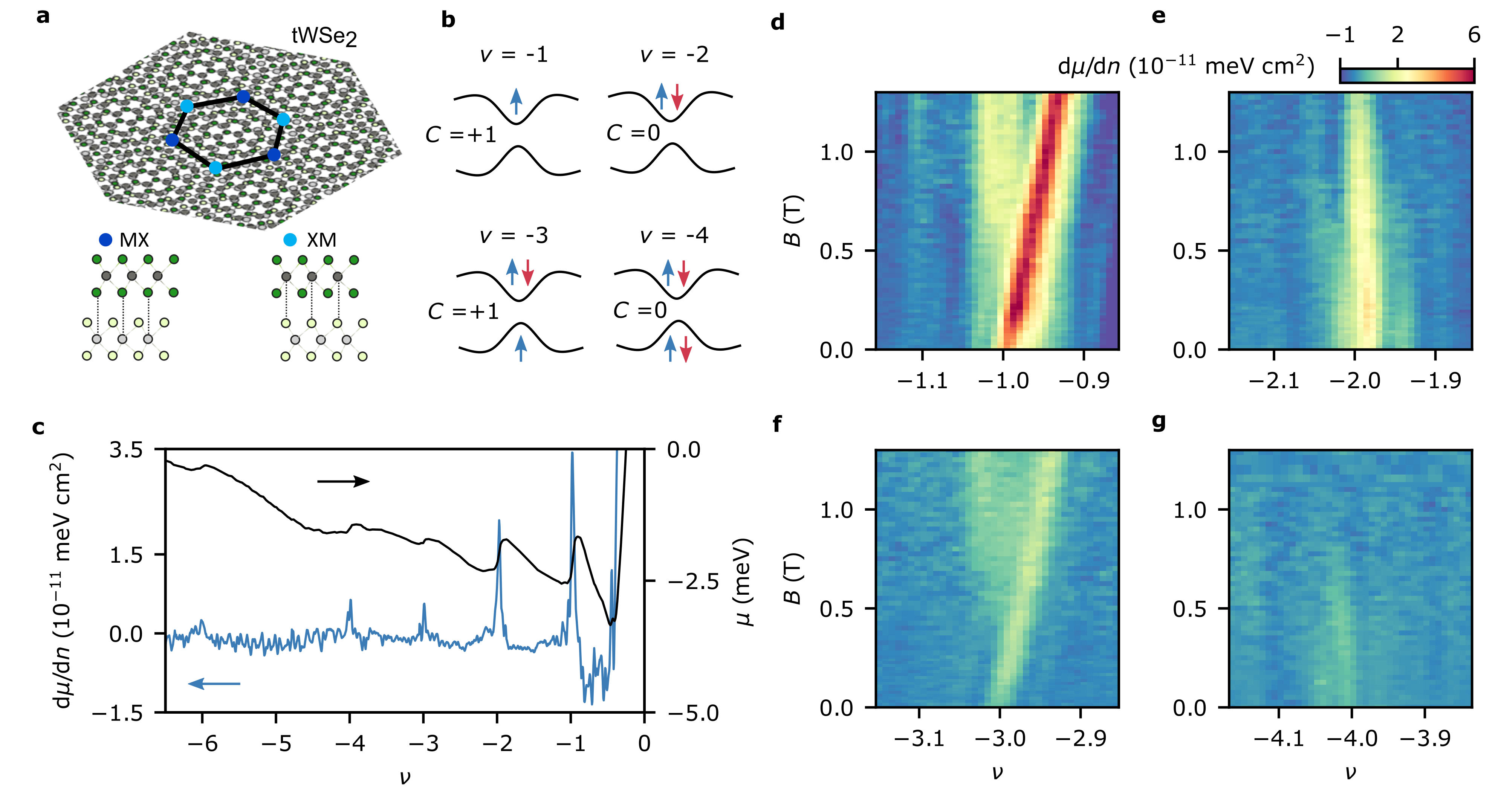
We study a twisted WSe2 bilayer with a small relative angle . At these twist angles, the lowest two moiré valence bands are well-described by a tight-binding model on a honeycomb lattice consisting of states localized at the XM and MX sites, shown schematically in Fig. 1a devakul_magic_2021 . We first focus on an area of the sample with . Figure 1c shows the chemical potential and the inverse electronic compressibility dd as a function of moiré filling factor , where signifies one hole per moiré unit cell. Gapped states occur at , and , superimposed on an overall downslope in , which reflects long-range electronic interactions near the valence band edge eisenstein_negative_1992 ; foutty_tunable_2023 .
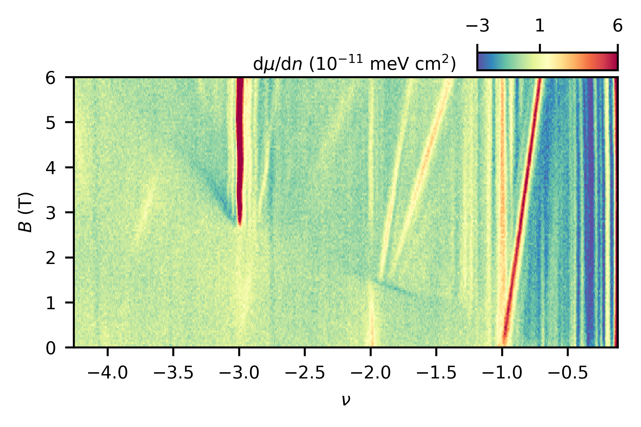
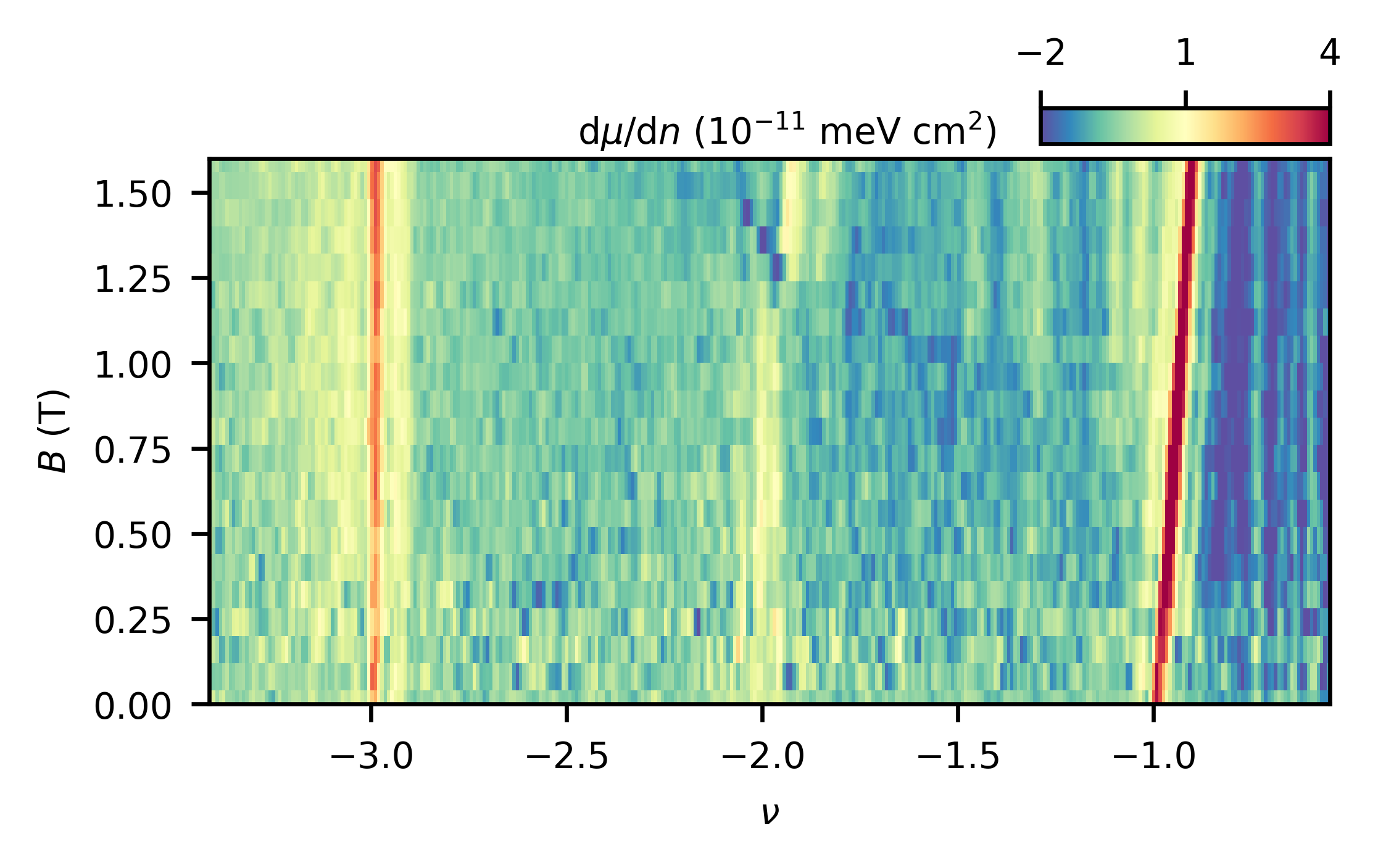
To determine the nature of the insulating states, we probe the behavior near integer fillings at low magnetic field and temperature mK (Fig. 1d-g). The slopes of the gaps encode their topological character (and Hall conductance) via the Streda formula streda_theory_1982 . At and , the gaps have slopes corresponding to Chern number all the way down to zero magnetic field, indicating that both are QAH states (Supplementary Sec. 1). At the even integers and , we measure gaps with total Chern number . Based on the observed nontrivial topology at odd integer fillings, these gaps are likely to be quantum spin Hall insulators with either two or four copies of fully filled bands (Fig. 1b). We measure broadly similar behavior at K (Extended Data Fig. 1) and across a wide spatial region (roughly 600 nm 1 m) in our sample with uniform twist angle between and (Extended Data Figs. 2,3).
To the best of our knowledge, this is the only moiré system reported to have multiple topological bands that are not related by degenerate quantum degrees of freedom. Our experiment is most consistent with the pair of lowest energy moiré bands having identical Chern number in a single spin-valley sector (see Supplementary Sec. 2 for further discussion). This is beyond any two-band tight binding model (which must have zero total Chern number), highlighting that the topological structure in tWSe2 extends beyond the Kane-Mele model.
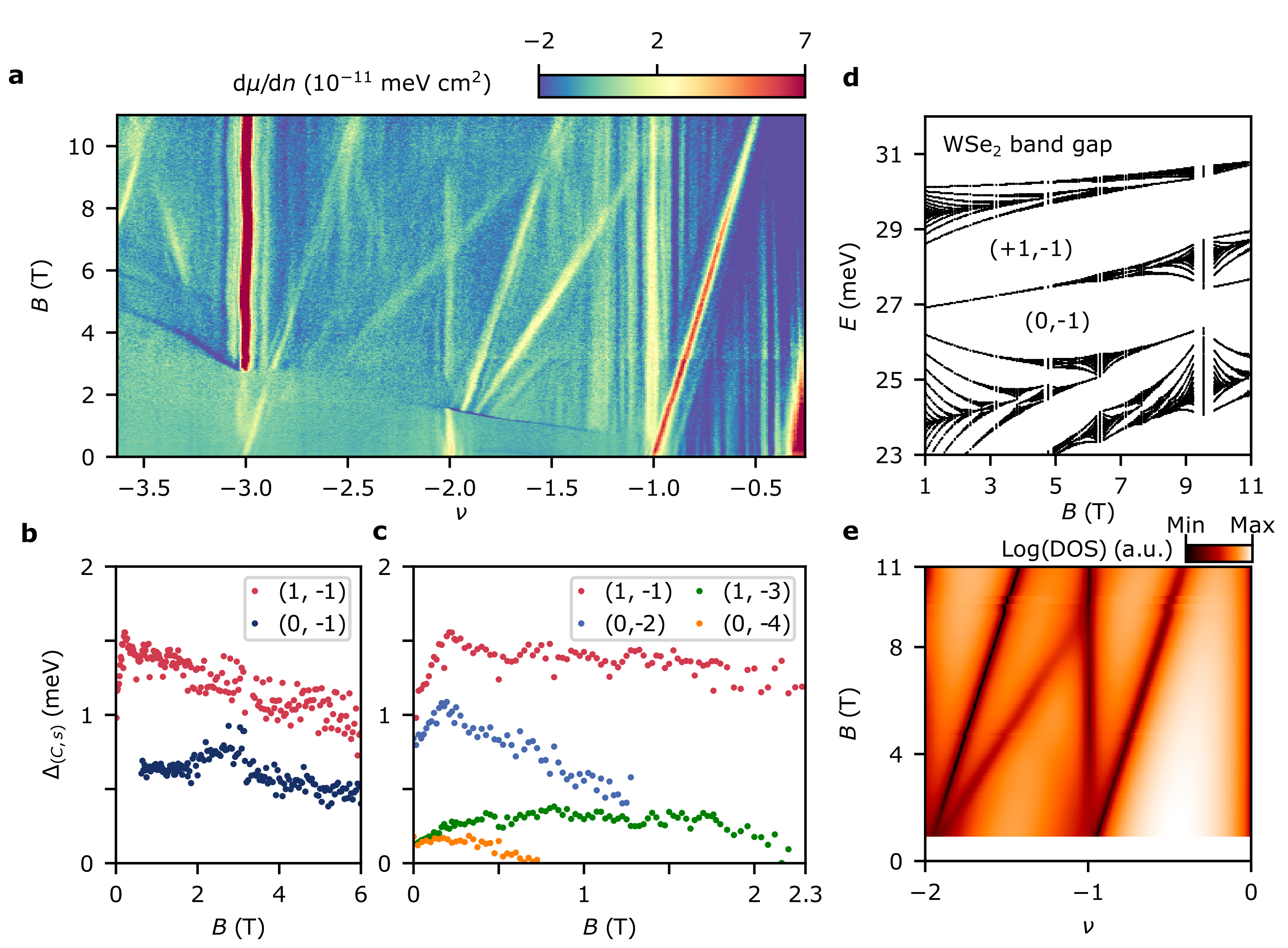
In Fig. 2a, we present the full magnetic field dependence at this twist angle up to T. A feature of both Chern insulating states at and is the coexistence of topologically trivial states emerging at relatively low magnetic fields T, where no other Landau levels (Hofstadter states) are seen. The thermodynamic charge gap (Methods) of the trivial state is smaller, and both gaps shrink in moderate magnetic fields (Fig. 2b). This behavior is consistent with theoretical expectations for Chern bands close to a topological band inversion (Fig. 2d-e), for which a Landau level is pinned to the top of the second moiré band, leading to two dominant Hofstadter gaps originating from .
At moderate magnetic fields, multiple additional Hofstadter states emerge. Each of these can be described by the Diophantine equation , where is the Chern number of the gap, is the flux quantum, and is the intercept. Some features of the observed Hofstadter pattern are not readily understood from the expected degeneracies of the bands. For example, the state is comparatively weak and is not resolved at high fields, inconsistent with a series of singly degenerate Hofstadter states emanating from an interaction-driven spin/valley polarized gap at . In addition to the Hofstadter states, we observe phase transitions as a function of magnetic field (and density), signified by sharp negative compressibility and changes in the pattern and/or strength of gaps such as that near at T. This likely reflects changing energetics between distinct moiré bands in a magnetic field cao_correlated_2018 ; kometter_hofstadter_2022 .
The magnitudes of the dominant gaps emanating from integer fillings exhibit nontrivial dependence at low magnetic fields (Fig. 2c). All of these gaps are non-monotonic below T. This is particularly stark at and , where the gaps sharply increase up to T, before decreasing beyond that field. One explanation for this gap dependence might be changes in the spin ordering of the ground states at very low magnetic fields. However, given the topology of the gap and the theoretically predicted spin-valley polarization of the QAH state, this is unlikely. Another possibility is a change in the nature of the lowest energy excitations, such as their spin configuration, as a field is applied. We note that the non-monotonic dependence of the gaps at and persists to angles where all states are topologically trivial (Extended Data Fig. 4).
III Twist angle dependence
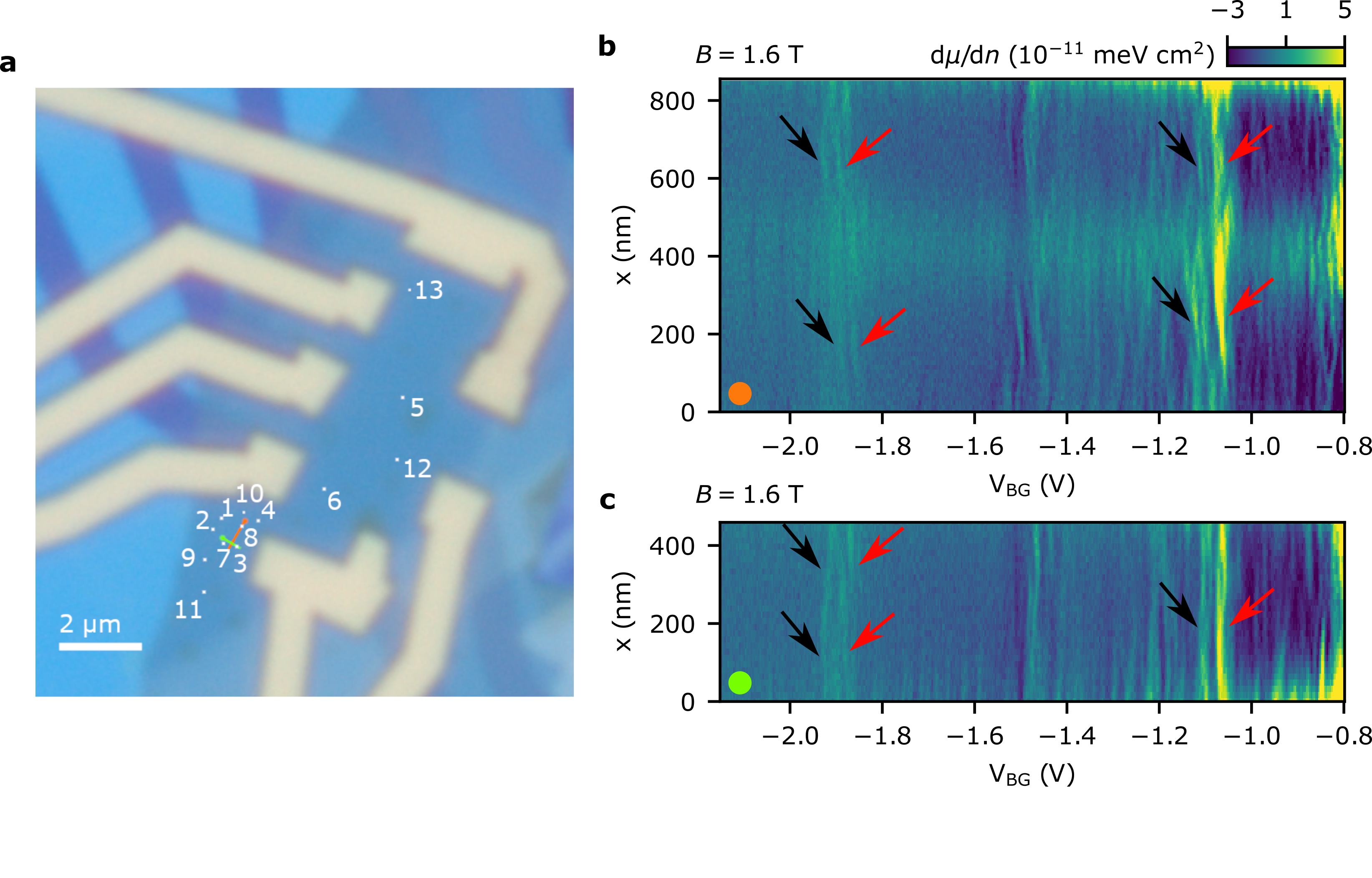
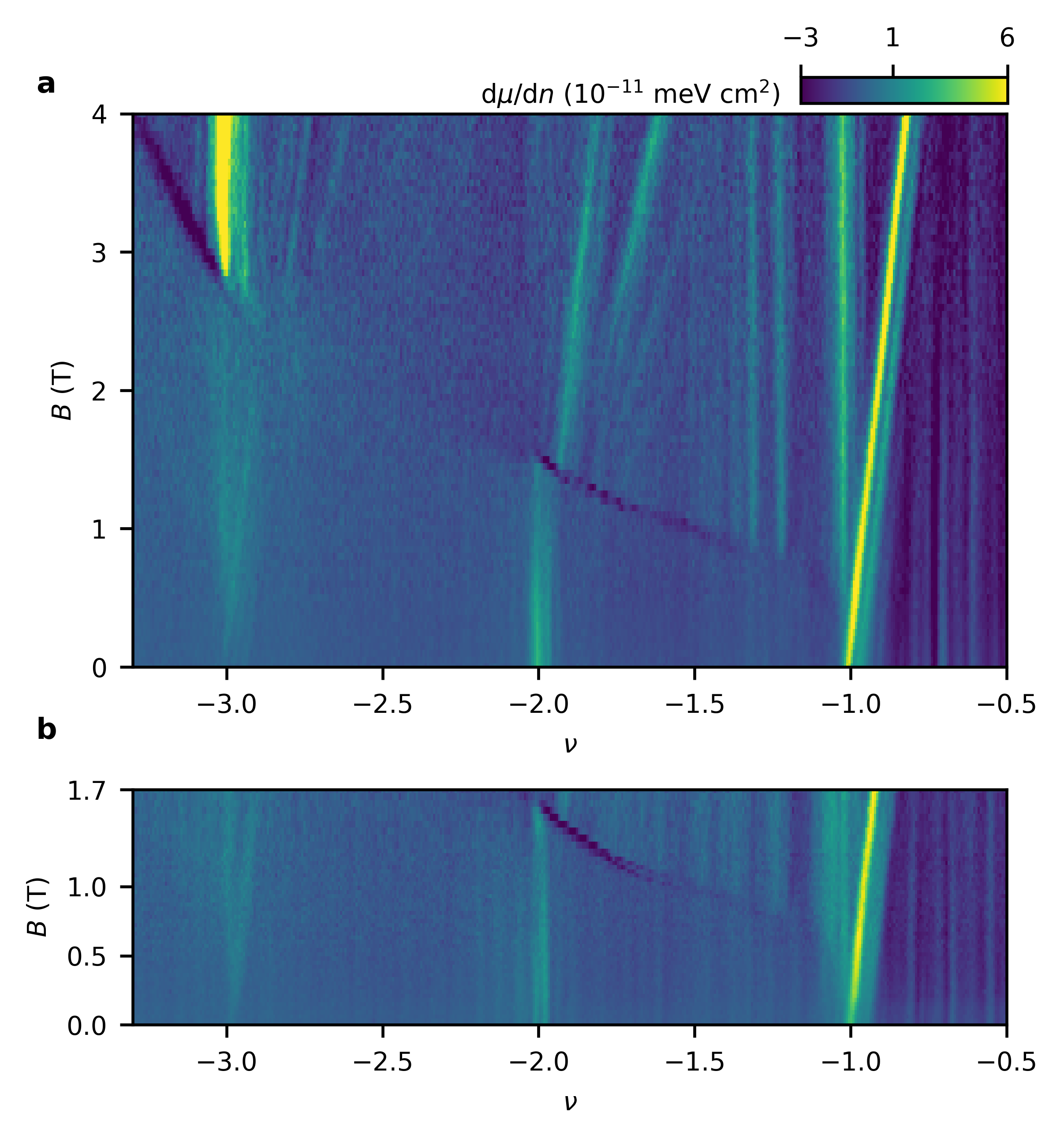
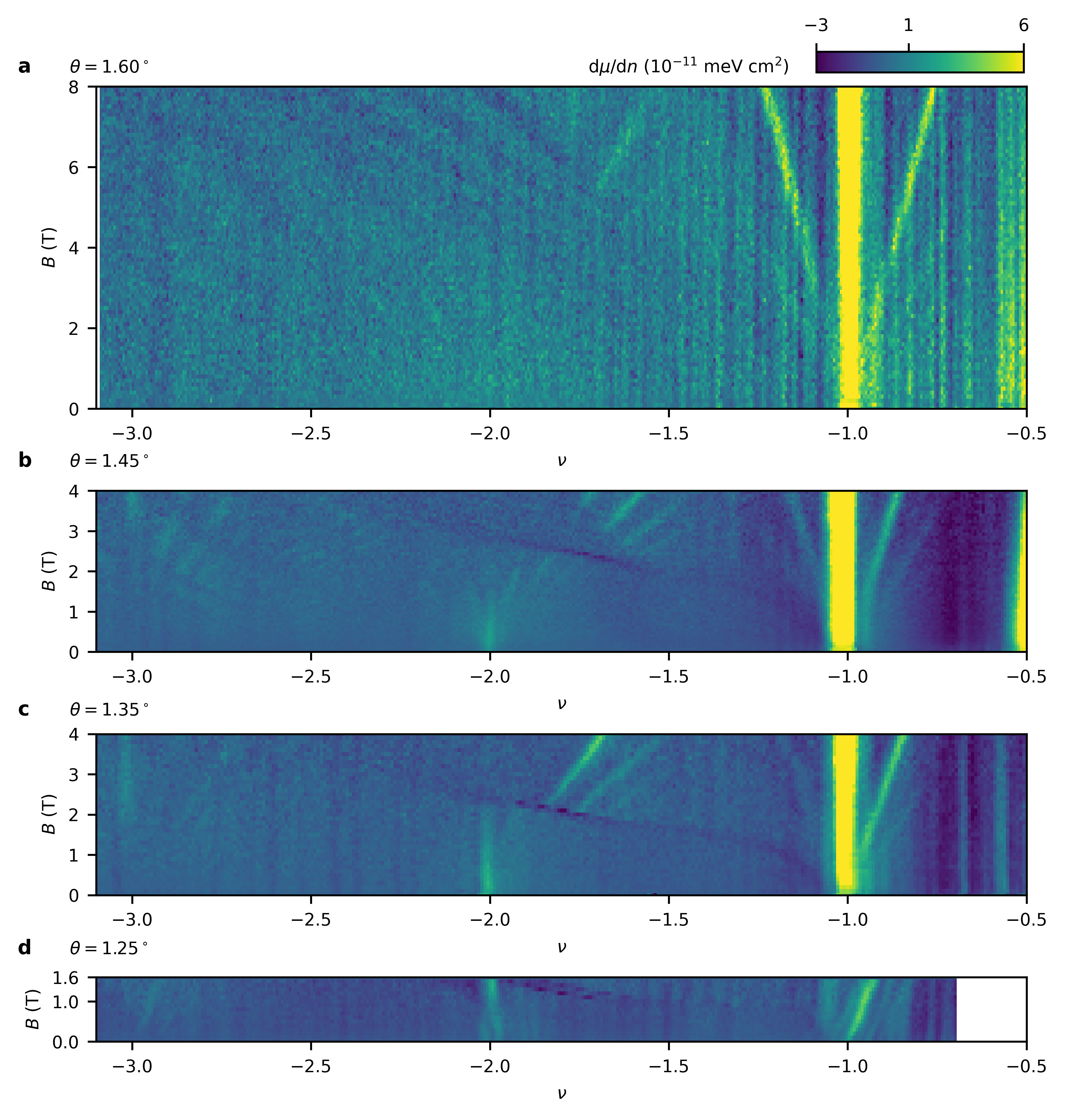
Measurements at other locations with local angles ranging from enable us to systematically investigate how these states depend on moiré wavelength. We present d/d as a function of up to T at a selection of different twist angles in Fig. 3a, with the observed incompressible states schematically depicted in the adjacent Wannier diagrams. Outside of a small range of angles () we do not observe any zero-field Chern insulators. At , we find that a QAH state is favored at , but not , indicating a slight difference in the twist angle dependence of these two states (Extended Data Fig. 5). Qualitatively, below this range, the integer gaps become much stronger, and fewer Hofstadter states are observed. Additionally there is a reversal of the relative gap strengths: at low twist angle, becomes larger than the , likely due to details of the interaction strength relative to the single-particle gap between moiré bands. The overall level of disorder also consistently appears worse, which may reflect an enhanced susceptibility to local atomic reconstruction at low angles. For , no zero-field gaps are observed at , and the gap vanishes at lower magnetic fields with increasing angle. Additionally, we observe a larger number of (weaker) Hofstadter states tracing back to all integers.
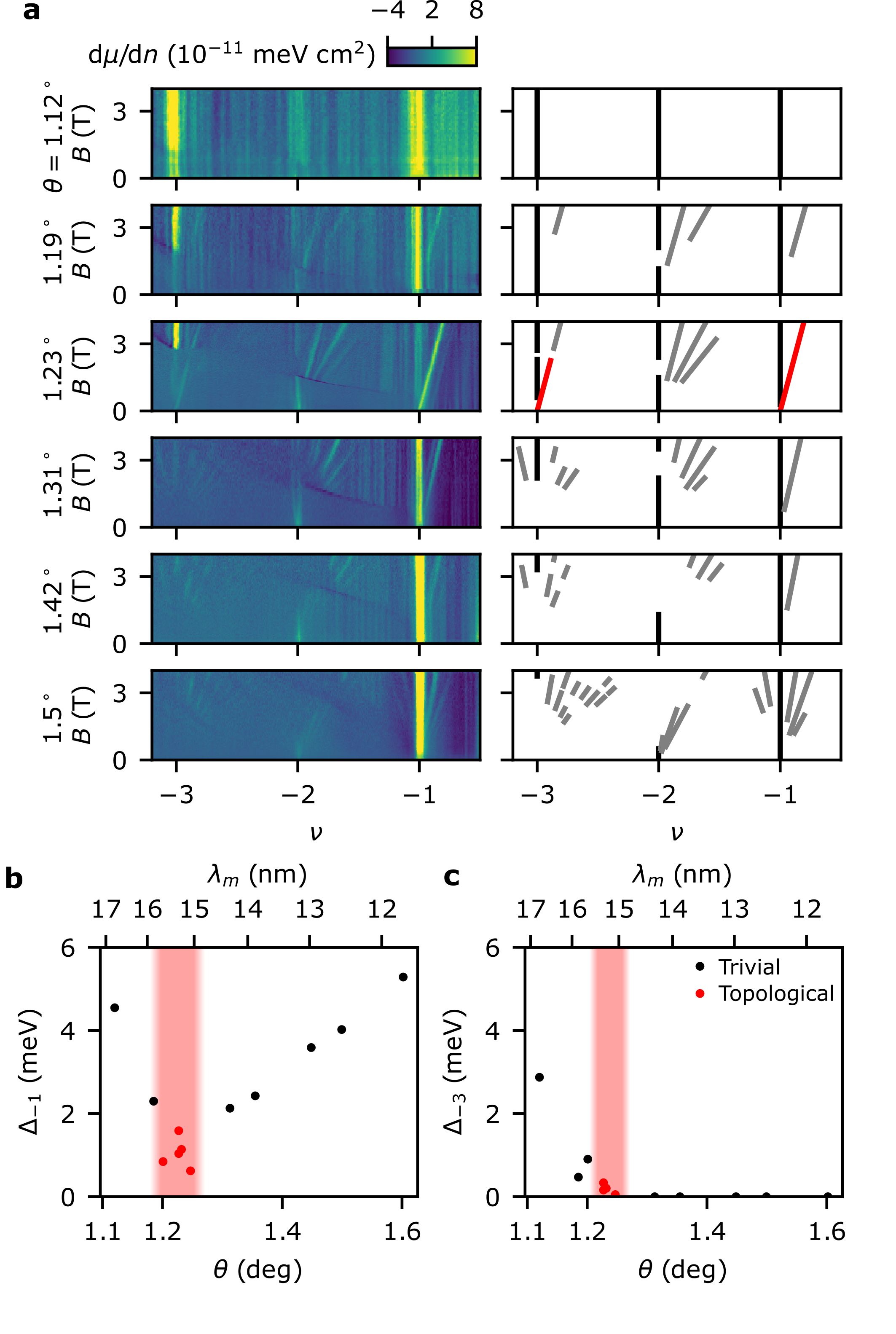
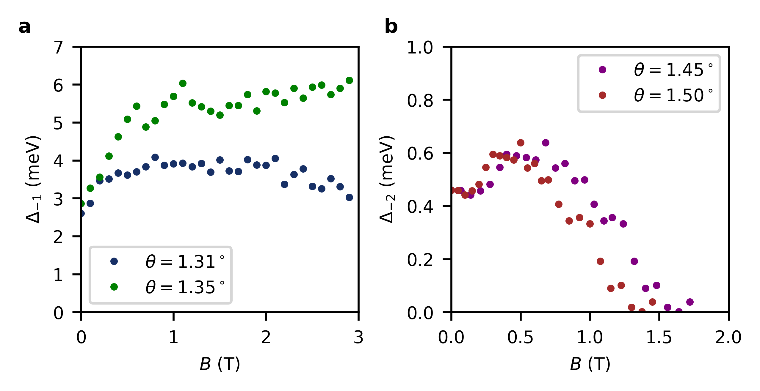
These data, along with more measurements at intermediate twists (Extended Data Figs. 3,6), allow us to quantify gap size dependence on twist angle at zero magnetic field, and to correlate it with the nature of the ground states that we observe. At , topological gaps appear at an overall minimum of a non-monotonic dependence of as a function of twist angle (Fig. 3b). This is consistent with a pair of twist-tuned band inversions. In contrast, the trend is generally monotonic as a function of angle at , and the gap only becomes topological just as it closes (Fig. 3c). At higher twist angles, interactions are likely not strong enough to induce an insulating state, so we realize a (trivial) insulator to QAH insulator to metal transition as a function of increasing twist angle at .
IV Topological phase transition at
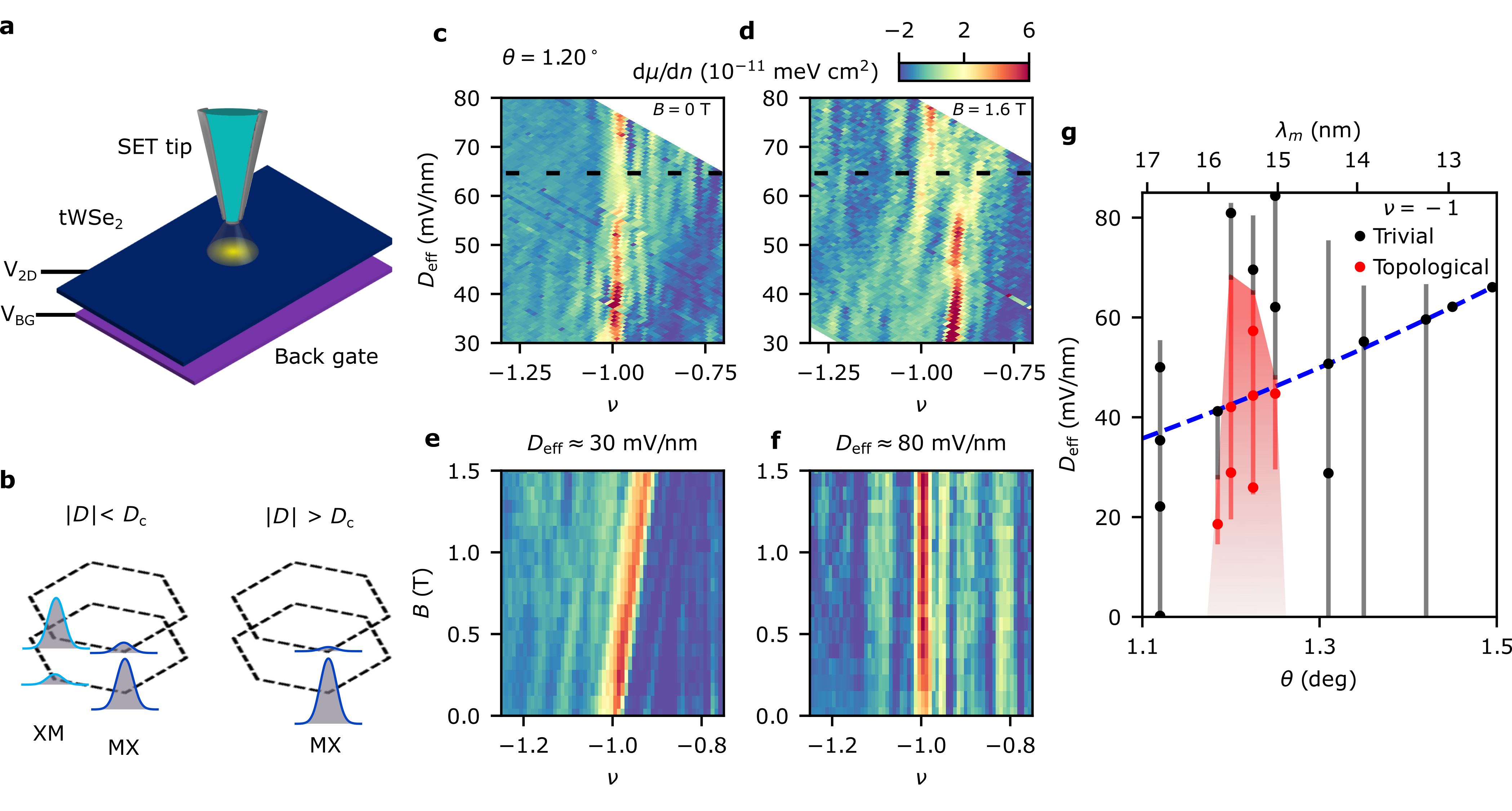
Theoretical predictions assert that the topological phase at is highly sensitive to an applied electric field, which favors polarization onto one of the layers and breaks the honeycomb sublattice symmetry of the emergent generalized Kane-Mele bands (Fig. 4b) devakul_magic_2021 . Though the scanning SET tip is generally noninvasive, if the d.c. sample voltage is adjusted, the tip can locally dope the region underneath it. We find that within certain bounds of , the tip acts as an effective gate that tunes the local displacement field applied to the sample (Fig. 4a, Methods). Remarkably, we observe a transition at as a function of at certain twist angles.
We focus on a location with . At , the gap at first decreases before re-emerging and strengthening as is increased (Fig. 4c). At T, states with different occur at different density. At lower , the state is dominant, while the state strengthens at high (Fig. 4d). At both magnetic fields, the change in behavior occurs at a similar critical displacement field around mV/nm (Fig. 4c-d, black dashed line). This suggests a phase transition from a topological state below to a trivial gap at higher displacement fields. The observations at both magnetic fields are consistent with the thermodynamic gap closing and reopening across , as expected from a topological quantum phase transition hasan_colloquium_2010 ; li_quantum_2021 .
To confirm this interpretation, we measure d/d as a function of magnetic field at different effective displacement fields. In Fig. 4e, we present a measurement at the same location with a small displacement field mV/nm. The resulting state is topological, with the gap continuing down to . However, when the displacement field is increased to mV/nm, a field sweep in the same location shows a topologically trivial gap (Fig. 4f).
By repeating similar measurements at other locations, we build up a phase diagram of the topological behavior at as a function of twist angle and applied displacement field (Fig. 4g). In this plot, vertical lines signify measurements as a function of , while points signify field sweeps to confirm the topological character of each state. In addition to being able to tune the topological gaps to trivial at , we are also able to induce topological states where trivial states had been favored (at ) by decreasing the applied displacement field (Supplementary Sec. 3). The range of twist angles over which we observe topological behavior is quite sharp, likely due to other competitive states at .
We perform Hartree-Fock calculations for the continuum model (Supplementary Sec. 2) which indicate a rich landscape of correlated ground states at integer . Within a certain range of twist angles at , a spin-valley polarized Chern insulator is expected to be favored, with transitions to a topologically trivial layer-polarized state at sufficiently high or low . At higher twist angle, our calculations predict that the Chern state will give way to an intervalley-coherent trivial state. Additionally, we find a quantum spin Hall insulator at , and a Chern insulator at with the same sign as at , as observed in experiment.
V Outlook
In conclusion, we have established twisted WSe2 as a platform to realize multiple topologically nontrivial bands which support symmetry-broken QAH gaps at half-filling. Comparing data across a range of moiré wavelengths from approximately 12 to 17 nm, we reveal widely varying correlated ground states of the honeycomb lattice model in twisted WSe2, both in magnitudes of the gaps and their topological character. This highlights the importance of moiré wavelength as a tuning parameter, which is only accessible in low-twist lattice-matched systems. Our work motivates further studies to confirm the specific spin-valley symmetry breaking of the odd-integer gaps, as well as transport studies to confirm that quantum spin Hall insulating states are realized at even integers, including a potential double quantum spin Hall insulator at mai_14_2023 . More generally, this work opens a new platform for studying tunable topological bands in the limit of larger moiré wavelengths where interacting phases such as fractional Chern insulators may be more readily stabilized crepel_anomalous_2022 ; morales-duran_pressure–enhanced_2023 .
Note added: While finalizing this manuscript, we became aware of a preprint that reports a topological moiré band and evidence of (fractional) quantum anomalous Hall states in twisted homobilayer MoTe2 cai_signatures_2023 .
References
- (1) Bloch, I., Dalibard, J. & Nascimbène, S. Quantum simulations with ultracold quantum gases. Nature Physics 8, 267–276 (2012). URL https://www.nature.com/articles/nphys2259. Number: 4 Publisher: Nature Publishing Group.
- (2) Kennes, D. M. et al. Moiré heterostructures as a condensed-matter quantum simulator. Nature Physics 17, 155–163 (2021). URL https://www.nature.com/articles/s41567-020-01154-3. Number: 2 Publisher: Nature Publishing Group.
- (3) Andrei, E. Y. & MacDonald, A. H. Graphene bilayers with a twist. Nature Materials 19, 1265–1275 (2020). URL https://www.nature.com/articles/s41563-020-00840-0. Number: 12 Publisher: Nature Publishing Group.
- (4) Balents, L., Dean, C. R., Efetov, D. K. & Young, A. F. Superconductivity and strong correlations in moiré flat bands. Nature Physics 16, 725–733 (2020). URL https://www.nature.com/articles/s41567-020-0906-9. Number: 7 Publisher: Nature Publishing Group.
- (5) Cao, Y. et al. Correlated insulator behaviour at half-filling in magic-angle graphene superlattices. Nature 556, 80–84 (2018). URL https://www.nature.com/articles/nature26154. Number: 7699 Publisher: Nature Publishing Group.
- (6) Cao, Y. et al. Unconventional superconductivity in magic-angle graphene superlattices. Nature 556, 43–50 (2018). URL https://www.nature.com/articles/nature26160%3C. Number: 7699 Publisher: Nature Publishing Group.
- (7) Mak, K. F. & Shan, J. Semiconductor moiré materials. Nature Nanotechnology 17, 686–695 (2022). URL https://www.nature.com/articles/s41565-022-01165-6. Number: 7 Publisher: Nature Publishing Group.
- (8) Wu, F., Lovorn, T., Tutuc, E. & MacDonald, A. Hubbard Model Physics in Transition Metal Dichalcogenide Moiré Bands. Physical Review Letters 121, 026402 (2018). URL https://link.aps.org/doi/10.1103/PhysRevLett.121.026402.
- (9) Zhang, Y., Yuan, N. F. Q. & Fu, L. Moir\’e quantum chemistry: Charge transfer in transition metal dichalcogenide superlattices. Physical Review B 102, 201115 (2020). URL https://link.aps.org/doi/10.1103/PhysRevB.102.201115. Publisher: American Physical Society.
- (10) Tang, Y. et al. Simulation of Hubbard model physics in WSe2/WS2 moiré superlattices. Nature 579, 353–358 (2020). URL https://www.nature.com/articles/s41586-020-2085-3. Number: 7799 Publisher: Nature Publishing Group.
- (11) Lau, C. N., Bockrath, M. W., Mak, K. F. & Zhang, F. Reproducibility in the fabrication and physics of moiré materials. Nature 602, 41–50 (2022). URL https://www.nature.com/articles/s41586-021-04173-z. Number: 7895 Publisher: Nature Publishing Group.
- (12) Xu, Y. et al. Correlated insulating states at fractional fillings of moiré superlattices. Nature 587, 214–218 (2020). URL https://www.nature.com/articles/s41586-020-2868-6.
- (13) Regan, E. C. et al. Mott and generalized Wigner crystal states in WSe2/WS2 moiré superlattices. Nature 579, 359–363 (2020). URL https://www.nature.com/articles/s41586-020-2092-4. Number: 7799 Publisher: Nature Publishing Group.
- (14) Li, T. et al. Continuous Mott transition in semiconductor moiré superlattices. Nature 597, 350–354 (2021). URL https://www.nature.com/articles/s41586-021-03853-0.
- (15) Li, T. et al. Quantum anomalous Hall effect from intertwined moiré bands. Nature 600, 641–646 (2021). URL https://www.nature.com/articles/s41586-021-04171-1. Number: 7890 Publisher: Nature Publishing Group.
- (16) Li, T. et al. Charge-order-enhanced capacitance in semiconductor moiré superlattices. Nature Nanotechnology 16, 1068–1072 (2021). URL http://www.nature.com/articles/s41565-021-00955-8.
- (17) Wang, L. et al. Correlated electronic phases in twisted bilayer transition metal dichalcogenides. Nature Materials 19, 861–866 (2020). URL https://www.nature.com/articles/s41563-020-0708-6. Number: 8 Publisher: Nature Publishing Group.
- (18) Ghiotto, A. et al. Quantum criticality in twisted transition metal dichalcogenides. Nature 597, 345–349 (2021). URL https://www.nature.com/articles/s41586-021-03815-6.
- (19) Xu, Y. et al. A tunable bilayer Hubbard model in twisted WSe2. Nature Nanotechnology 17, 934–939 (2022). URL https://www.nature.com/articles/s41565-022-01180-7. Number: 9 Publisher: Nature Publishing Group.
- (20) Serlin, M. et al. Intrinsic quantized anomalous Hall effect in a moiré heterostructure. Science 367, 900–903 (2020). URL https://www.science.org/doi/abs/10.1126/science.aay5533. Publisher: American Association for the Advancement of Science.
- (21) Chen, G. et al. Tunable correlated Chern insulator and ferromagnetism in a moiré superlattice. Nature 579, 56–61 (2020). URL https://www.nature.com/articles/s41586-020-2049-7. Number: 7797 Publisher: Nature Publishing Group.
- (22) Pierce, A. T. et al. Unconventional sequence of correlated Chern insulators in magic-angle twisted bilayer graphene. Nature Physics 17, 1210–1215 (2021). URL https://www.nature.com/articles/s41567-021-01347-4. Number: 11 Publisher: Nature Publishing Group.
- (23) Polshyn, H. et al. Electrical switching of magnetic order in an orbital Chern insulator. Nature 588, 66–70 (2020). URL https://www.nature.com/articles/s41586-020-2963-8. Number: 7836 Publisher: Nature Publishing Group.
- (24) Stepanov, P. et al. Competing Zero-Field Chern Insulators in Superconducting Twisted Bilayer Graphene. Physical Review Letters 127, 197701 (2021). URL https://link.aps.org/doi/10.1103/PhysRevLett.127.197701.
- (25) Kane, C. L. & Mele, E. J. Quantum Spin Hall Effect in Graphene. Physical Review Letters 95, 226801 (2005). URL https://link.aps.org/doi/10.1103/PhysRevLett.95.226801. Publisher: American Physical Society.
- (26) Wu, F., Lovorn, T., Tutuc, E., Martin, I. & MacDonald, A. Topological Insulators in Twisted Transition Metal Dichalcogenide Homobilayers. Physical Review Letters 122, 086402 (2019). URL https://link.aps.org/doi/10.1103/PhysRevLett.122.086402. Publisher: American Physical Society.
- (27) Devakul, T., Crépel, V., Zhang, Y. & Fu, L. Magic in twisted transition metal dichalcogenide bilayers. Nature Communications 12, 6730 (2021). URL https://www.nature.com/articles/s41467-021-27042-9. Number: 1 Publisher: Nature Publishing Group.
- (28) Pan, H., Wu, F. & Das Sarma, S. Band topology, Hubbard model, Heisenberg model, and Dzyaloshinskii-Moriya interaction in twisted bilayer ${\mathrm{WSe}}_{2}$. Physical Review Research 2, 033087 (2020). URL https://link.aps.org/doi/10.1103/PhysRevResearch.2.033087. Publisher: American Physical Society.
- (29) Tschirhart, C. L. et al. Intrinsic spin Hall torque in a moiré Chern magnet. Nature Physics 1–7 (2023). URL https://www.nature.com/articles/s41567-023-01979-8. Publisher: Nature Publishing Group.
- (30) Zhao, W. et al. Realization of the Haldane Chern insulator in a moir\’e lattice (2022). URL http://arxiv.org/abs/2207.02312. ArXiv:2207.02312 [cond-mat].
- (31) Tao, Z. et al. Valley-coherent quantum anomalous Hall state in AB-stacked MoTe2/WSe2 bilayers (2022). URL http://arxiv.org/abs/2208.07452. ArXiv:2208.07452 [cond-mat].
- (32) Zhang, Y., Devakul, T. & Fu, L. Spin-textured Chern bands in AB-stacked transition metal dichalcogenide bilayers. Proceedings of the National Academy of Sciences 118, e2112673118 (2021). URL https://www.pnas.org/doi/full/10.1073/pnas.2112673118. Publisher: Proceedings of the National Academy of Sciences.
- (33) Xie, Y.-M., Zhang, C.-P., Hu, J.-X., Mak, K. F. & Law, K. Valley-Polarized Quantum Anomalous Hall State in Moir\’e ${\mathrm{MoTe}}_{2}/{\mathrm{WSe}}_{2}$ Heterobilayers. Physical Review Letters 128, 026402 (2022). URL https://link.aps.org/doi/10.1103/PhysRevLett.128.026402. Publisher: American Physical Society.
- (34) Pan, H., Xie, M., Wu, F. & Das Sarma, S. Topological Phases in AB-Stacked ${\mathrm{MoTe}}_{2}/{\mathrm{WSe}}_{2}$: ${\mathbb{Z}}_{2}$ Topological Insulators, Chern Insulators, and Topological Charge Density Waves. Physical Review Letters 129, 056804 (2022). URL https://link.aps.org/doi/10.1103/PhysRevLett.129.056804. Publisher: American Physical Society.
- (35) Devakul, T. & Fu, L. Quantum Anomalous Hall Effect from Inverted Charge Transfer Gap. Physical Review X 12, 021031 (2022). URL https://link.aps.org/doi/10.1103/PhysRevX.12.021031. Publisher: American Physical Society.
- (36) Rademaker, L. Spin-orbit coupling in transition metal dichalcogenide heterobilayer flat bands. Physical Review B 105, 195428 (2022). URL https://link.aps.org/doi/10.1103/PhysRevB.105.195428. Publisher: American Physical Society.
- (37) Dong, Z. & Zhang, Y.-H. Excitonic Chern insulator and kinetic ferromagnetism in a ${\mathrm{MoTe}}_{2}/{\mathrm{WSe}}_{2}$ moir\’e bilayer. Physical Review B 107, L081101 (2023). URL https://link.aps.org/doi/10.1103/PhysRevB.107.L081101. Publisher: American Physical Society.
- (38) Mai, P., Huang, E. W., Yu, J., Feldman, B. E. & Phillips, P. W. Interaction-driven spontaneous ferromagnetic insulating states with odd Chern numbers. npj Quantum Materials 8, 1–7 (2023). URL https://www.nature.com/articles/s41535-023-00544-z. Number: 1 Publisher: Nature Publishing Group.
- (39) Mai, P., Zhao, J., Feldman, B. E. & Phillips, P. W. 1/4 is the new 1/2: Interaction-induced Unification of Quantum Anomalous and Spin Hall Effects (2023). URL http://arxiv.org/abs/2210.11486. ArXiv:2210.11486 [cond-mat].
- (40) Eisenstein, J. P., Pfeiffer, L. N. & West, K. W. Negative compressibility of interacting two-dimensional electron and quasiparticle gases. Physical Review Letters 68, 674–677 (1992). URL https://link.aps.org/doi/10.1103/PhysRevLett.68.674.
- (41) Foutty, B. A. et al. Tunable spin and valley excitations of correlated insulators in -valley moiré bands. Nature Materials 1–6 (2023). URL https://www.nature.com/articles/s41563-023-01534-z. Publisher: Nature Publishing Group.
- (42) Streda, P. Theory of quantised Hall conductivity in two dimensions. Journal of Physics C: Solid State Physics 15, L717 (1982). URL https://dx.doi.org/10.1088/0022-3719/15/22/005.
- (43) Kometter, C. R. et al. Hofstadter states and reentrant charge order in a semiconductor moir\’e lattice (2022). URL http://arxiv.org/abs/2212.05068. ArXiv:2212.05068 [cond-mat].
- (44) Hasan, M. Z. & Kane, C. L. Colloquium: Topological insulators. Reviews of Modern Physics 82, 3045–3067 (2010). URL https://link.aps.org/doi/10.1103/RevModPhys.82.3045. Publisher: American Physical Society.
- (45) Crépel, V. & Fu, L. Anomalous Hall metal and fractional Chern insulator in twisted transition metal dichalcogenides (2022). URL http://arxiv.org/abs/2207.08895. ArXiv:2207.08895 [cond-mat].
- (46) Morales-Durán, N. et al. Pressure–enhanced fractional Chern insulators in moir\’e transition metal dichalcogenides along a magic line (2023). URL http://arxiv.org/abs/2304.06669. ArXiv:2304.06669 [cond-mat].
- (47) Cai, J. et al. Signatures of Fractional Quantum Anomalous Hall States in Twisted MoTe2 Bilayer (2023). URL http://arxiv.org/abs/2304.08470. ArXiv:2304.08470 [cond-mat].
- (48) Movva, H. C. P. et al. High-Mobility Holes in Dual-Gated WSe2 Field-Effect Transistors. ACS Nano 9, 10402–10410 (2015). URL https://doi.org/10.1021/acsnano.5b04611. Publisher: American Chemical Society.
- (49) Yu, J. et al. Correlated Hofstadter spectrum and flavour phase diagram in magic-angle twisted bilayer graphene. Nature Physics 18, 825–831 (2022). URL https://www.nature.com/articles/s41567-022-01589-w. Number: 7 Publisher: Nature Publishing Group.
- (50) McGilly, L. J. et al. Visualization of moiré superlattices. Nature Nanotechnology 15, 580–584 (2020). URL https://www.nature.com/articles/s41565-020-0708-3. Number: 7 Publisher: Nature Publishing Group.
- (51) Bai, Y. et al. Excitons in strain-induced one-dimensional moiré potentials at transition metal dichalcogenide heterojunctions. Nature Materials 19, 1068–1073 (2020). URL https://www.nature.com/articles/s41563-020-0730-8. Number: 10 Publisher: Nature Publishing Group.
- (52) Zondiner, U. et al. Cascade of phase transitions and Dirac revivals in magic-angle graphene. Nature 582, 203–208 (2020). URL https://www.nature.com/articles/s41586-020-2373-y.
- (53) Uri, A. et al. Mapping the twist-angle disorder and Landau levels in magic-angle graphene. Nature 581, 47–52 (2020). URL https://www.nature.com/articles/s41586-020-2255-3. Number: 7806 Publisher: Nature Publishing Group.
- (54) Eisenstein, J. P., Pfeiffer, L. N. & West, K. W. Compressibility of the two-dimensional electron gas: Measurements of the zero-field exchange energy and fractional quantum Hall gap. Physical Review B 50, 1760–1778 (1994). URL https://link.aps.org/doi/10.1103/PhysRevB.50.1760.
VI Methods
VI.1 Sample fabrication
The tWSe2 device was fabricated using standard dry transfer techniques. Using a poly(bisphenol A carbonate) (PC)/polydimethylsiloxane (PDMS) stamp, we pick up a thin (15 nm thick) hexagonal boron nitride (hBN) flake, followed by the first half of the monolayer WSe2 flake (exfoliated from HQ Graphene source), using the hBN to tear the flake in two, and then the second half rotated to a controlled angle of . Separately, we prepare a stack with a bottom hBN (13 nm) and a graphite (5 nm) back gate, on which we deposit pre-patterned Cr/Pt contacts (2 nm / 8 nm). This is annealed at C for 8 hours to clean polymer and resist residues both before and after pre-patterning of contacts. The tWSe2 stack is then dropped onto the pre-patterned contacts. We used standard e-beam lithography techniques to fabricate metallic contacts, as well as local “contact-gates” over the Pt contacts, while leaving the rest of the sample ungated on top for access to the SET movva_high-mobility_2015 ; foutty_tunable_2023 .
VI.2 SET Measurements
The SET sensor was fabricated by evaporating aluminum onto a pulled quartz rod, with an estimated diameter at the apex of nm. The SET “tip” is brought to about nm above the sample surface. Scanning SET measurements were performed in a Unisoku USM 1300 scanning probe microscope with a customized microscope head. a.c. excitations (2-5 mV peak-to-peak amplitude) were applied to both sample and back gate at distinct frequencies between 200 and 400 Hz. We then measure inverse compressibility where and are measurements of the SET current demodulated at respective frequencies of the back gate and sample excitations yu_correlated_2022 . Except where otherwise noted (Fig. 4), a d.c. offset voltage is applied to the sample to maintain the working point of the SET at its maximum sensitivity point within a Coulomb blockade oscillation fringe chosen to be near the “flat-band” condition where the tip does not gate the sample. This minimizes tip-induced doping and provides a direct measurement of at d.c. timescales. Depending on measurement location, we measure a small ( meV cm2) difference in d/d between a.c. and d.c. measurements, which we subtract from the a.c. in all data presented in the main text (see Supplementary Sec. 4 for further discussion). The contact gates are held at a large, negative voltage throughout the measurement to maintain good electrical contact across variable hole doping. All SET measurements are taken at mK unless otherwise noted.
VI.3 Density and twist angle determination
The approximate twist angle of the sample () is determined by the control over rotation in the stackng process. To ensure that the tWSe2 is not overly strained or relaxed after picking it up, we perform piezoelectric force microscopy (PFM) using a Bruker Icon atomic force microscope during the fabrication process on the PC slide before setting the stack onto the prepatterned Pt contacts mcgilly_visualization_2020 ; bai_excitons_2020 . We present this in Supplementary Sec. 5. We find a relatively low-strain triangular moiré superlattice with lattice constant around nm, consistent with what we extract from SET measurements.
As described in the main text, there is some variation in local twist angle across the device. We use SET measurements to precisely determine local angle in a similar manner to standard techniques in magic-angle twisted bilayer graphene zondiner_cascade_2020 ; uri_mapping_2020 . From the slopes of the Hofstadter states, we can accurately measure the sample capacitance and convert between back gate voltage and carrier density . We then use the integer gaps we measure (e.g. at , and ) and/or the corresponding Hofstadter intercepts (in cases where there is no zero-field gap) to determine the density corresponding to filling one hole per moiré unit cell. From this density , we convert to twist angle via and subsequently moiré wavelength via , where nm.
VI.4 Extraction of gap sizes
The thermodynamic gap sizes shown in the main text are given by the size of the step in the chemical potential . Practically, this is extracted by numerically integrating across the gap. To accurately measure the gap on top of the widespread negative compressibility coming from long-range interactions at low density, we subtract a small background before integrating, analogous to Refs. eisenstein_compressibility_1994 ; kometter_hofstadter_2022 . Generally, this background is taken from averaging the value of on either side of the gap. This background is measured sufficiently far (in density) from the gap so that chemical potential behavior immediately adjacent to the gap, for example enhanced negative compressibility, is not included in the background. In a few cases in which gaps are particularly close together (for example, gaps and gaps with between and T), the background is just taken from a single side of the gap, so that the behavior of one gap does not affect the extracted value of the other. In general, disorder can reduce the size of measured gaps. In the main text (Figs. 2-3), we present gaps from data measured at optimized locations that have low twist angle variability in order to minimize the effects of disorder in comparisons.
VI.5 Electric field tuning with SET
As mentioned in the main text, if the d.c. sample voltage is tuned away from the “flat-band” condition compensating for the work function difference between sample and tip, the tip will locally gate the sample. We can model this doping by treating the tip as one side of a parallel plate capacitor: , where is the back (top) gate capacitance, and are the d.c. voltages applied to sample and back gate, is the “flat-band” voltage at which the tip and sample are work-function-compensated, and is the voltage at which back gate and sample are work-function-compensated (equivalent to the voltage of the WSe2 band edge). While will depend on the height of the tip, we experimentally extract for the measurements shown in the main text based on the shifts of constant-density features in the plane. Data shown in Fig. 4c-d is taken by initially fixing and then sweeping , feeding back on the value of while data is taken to maintain the same position along the SET Coulomb blockade oscillation. From this data, we apply the transformation to convert to and from and .
VI.6 Hofstadter spectrum calculation
We compute the Hofstadter spectrum for the continuum model for TMD homobilayers wu_topological_2019 , with continuum model parameters extracted from ab initio calculations of Ref devakul_magic_2021 : . We use an effective mass , where is the electron mass, and a WSe2 lattice constant of Å. The calculation is performed at a twist angle and displacement field is modeled as an interlayer potential with meV. The continuum model is described in more detail in the Supplementary Sec. 2. The spectrum for the valley bands features a topological first band with that is close to a displacement field tuned band inversion with the second band.
The finite magnetic field is incorporated by minimal substitution with the symmetric gauge vector potential . At flux per unit cell , where is the moiré unit cell area, the Hamiltonian is diagonalized in the Landau level basis with a large cutoff , using the method described in detail in Ref kometter_hofstadter_2022 . The resulting Hofstadter spectrum shown in Fig. 2d is computed for the valley bands.
To compute the Wannier plot in Fig. 2e, we first apply a Gaussian broadening of width meV to the calculated density of states. The filling factor is obtained by integrating the broadened density of states from the charge neutrality point, assuming full valley polarization.
VII Data availability
The data that supports the findings of this study are available from the corresponding authors upon reasonable request.
VIII Code availability
The codes that support the findings of this study are available from the corresponding authors upon reasonable request.
IX Acknowledgements
Experimental work was primarily supported by the Department of Energy, Office of Basic Energy Sciences, award number DE-SC0023109. B.E.F. acknowledges an Alfred P. Sloan Foundation Fellowship and a Cottrell Scholar Award. The work at Massachusetts Institute of Technology was supported by the Air Force Office of Scientific Research (AFOSR) under award FA9550-22-1-0432. K.W. and T.T. acknowledge support from the JSPS KAKENHI (Grant Numbers 20H00354 and 23H02052) and World Premier International Research Center Initiative (WPI), MEXT, Japan. B.A.F. acknowledges a Stanford Graduate Fellowship. Part of this work was performed at the Stanford Nano Shared Facilities (SNSF), supported by the National Science Foundation under award ECCS-2026822.
X Author contribution
B.A.F. and C.R.K. conducted the scanning SET measurements. B.A.F. and B.E.F. designed the experiment. T.D., A.P.R., and L.F. conducted theoretical calculations. B.A.F. fabricated the sample. K.W. and T.T. provided the hBN crystals. B.E.F. and L.F. supervised the project. All authors participated in analysis of the data and writing of the manuscript.
XI Competing interests
The authors declare no competing interest.
XII Extended Data Figures