Correlative Imaging of Individual CsPbBr3 Nanocrystals: Role of Isolated Grains in Photoluminescence of Perovskite Polycrystalline Thin Films
Abstract
We report on the optical properties of CsPbBr3 polycrystalline thin film on a single grain level. A sample comprised of isolated nanocrystals (NCs) mimicking the properties of the polycrystalline thin film grains that can be individually probed by photoluminescence spectroscopy was prepared. These NCs were analyzed using correlative microscopy allowing the examination of structural, chemical, and optical properties from identical sites. Our results show that the stoichiometry of the CsPbBr3 NCs is uniform and independent of the NCs’ morphology. The photoluminescence (PL) peak emission wavelength is slightly dependent on the dimensions of NCs, with the blue shift up to 9 nm for the smallest analyzed NCs. The magnitude of the blueshift is smaller than the emission linewidth, thus detectable only by high-resolution PL mapping. By comparing the emission energies obtained from the experiment and a rigorous effective mass model we can fully attribute the observed variations to the size-dependent quantum confinement effect.
keywords:
lead halide perovskites, CsPbBr3, correlative high-resolution imaging, photoluminescence, polycrystalline thin film, isolated grainsCentral European Institute of Technology, Brno University of Technology, Purkyňova 123, 612 00 Brno, Czech Republic \alsoaffiliationCentral European Institute of Technology, Brno University of Technology, Purkyňova 123, 612 00 Brno, Czech Republic \altaffiliationTESCAN ORSAY HOLDING, a.s, Libušina tř. 21, Brno 623 00, Czech Republic \alsoaffiliationCentral European Institute of Technology, Brno University of Technology, Purkyňova 123, 612 00 Brno, Czech Republic \alsoaffiliationCentral European Institute of Technology, Brno University of Technology, Purkyňova 123, 612 00 Brno, Czech Republic \alsoaffiliationCentral European Institute of Technology, Brno University of Technology, Purkyňova 123, 612 00 Brno, Czech Republic \alsoaffiliationCentral European Institute of Technology, Brno University of Technology, Purkyňova 123, 612 00 Brno, Czech Republic \alsoaffiliationCentral European Institute of Technology, Brno University of Technology, Purkyňova 123, 612 00 Brno, Czech Republic \abbreviationsLHP, PL, NC
![[Uncaptioned image]](/html/2304.05114/assets/x1.png)
1 Introduction
Fully inorganic lead halide perovskite (LHP) CsPbBr3 is a semiconducting material with a direct band gap exhibiting unique optical properties, such as high internal and external quantum yields of both Stokes and anti-Stokes photoluminescence (PL), narrow PL linewidth, low non-radiative losses, remarkable photostability, and high PL emission wavelength tunability due to a strong quantum confinement effect (QCE) 1, 2, 3, 4, 5, 6, 7, 8, 9. For its unique optical properties, CsPbBr3 has emerged as a contemporary material that has fuelled further intensive development in the fields of optoelectronics, such as light-emitting devices 10, 11, single photon-emitters 12, photovoltaics 13, 14, 15, high-energy gamma radiation detectors 16, photocatalysis of chemical processes 17, high-resolution displays 18, non-linear optical wavelength converters 19, reconfigurable memristors 20, hyper-sensitive scintillators 21, 22, 23 or even functional metasurfaces 24. The exceptionality of CsPbBr3 originates from the unique electronic fine structure and high tolerance towards structural defects 25, 26. Moreover, due to the inherent ionic character of CsPbBr3, a cheap and facile fabrication of CsPbBr3 nanocrystals (NCs) is possible simply by mixing the corresponding precursor solutions without the need for elevated temperature or other, potentially challenging conditions 27. Hence, NCs and their thin films in general form the basis of halide perovskite-based optoelectronic devices with unique or improved optical and electronic properties 28. The optical and electronic properties of CsPbBr3 NCs are strongly dependent on their dimensions, morphology, size distribution and surface passivation 29, 30. Decreasing the size of CsPbBr3 crystals to the nanoscale or appropriate surface passivation can be utilized to tune or even enhance their optical properties 31, 32, 33, 34, 35, 36. A full control over the size of the colloidal lead halide perovskite nanocrystals (cn-LHP) and its distribution has been demonstrated by Protesescu et al., who presented a hot-injection method allowing the colloidal synthesis of well-defined, monodisperse and monocrystalline NCs with PL properties far exceeding the polycrystalline films (pf-LHP) 37.
However, cn-CsPbBr3 prepared by the hot-injection method suffer from a significant underperformance due to problems with electrical contacting which substantially limits their usage in optoelectronic devices in comparison to their polycrystalline film (pf-CsPbBr3) counterparts 38. Therefore, the prospect of long operational devices stability, high conversion efficiency (>25 %), and simple utilization in electroluminescent devices make pf-CsPbBr3 better candidates for today’s optoelectronic devices than cn-CsPbBr3, especially for solar cells technology 38, 39, 40, 41.
A suitable way to study the optical properties of pf-CsPbBr3 such as the emission wavelength, spectral broadening, recombination kinetics processes, and internal electrochemical potential of free charge carriers is through PL spectroscopy 1, 42, 43, 44, 45, 46. When correlated with the high-resolution imaging techniques of low-dimensional structures, PL spectroscopy provides a direct insight into the influence of local morphology effects 47 or the energy levels shift caused by QCE 48, 49, 50. However, due to the limited spatial resolution of optical microscopy, this approach cannot provide a response of individual grains of polycrystalline thin film, as there are usually several grains within the focus.
Here, we demonstrate a comprehensive analysis of the material properties of individual CsPbBr3 NCs prepared from a low-concentrated pf-LHPs solution while achieving considerable spacing between individual NCs. This system is representative for thin polycrystalline films, as it was grown under the conditions typically used for the growth of thin films. In contrast to the thin polycrystalline film with overlapping grains, the well-isolated NCs can be addressed individually by optical spectroscopy. A correlative approach based on focused ion beam (FIB) tagging of the examined area on the sample is used and the synergy of high-resolution experimental techniques is utilized: transmission electron microscopy (TEM), scanning electron microscopy (SEM), atomic force microscopy (AFM) and confocal optical spectroscopy (COS) together with anti-Stokes PL mapping. These techniques are capable of analysing CsPbBr3 NCs’ inner structure, determining their characteristic dimensions, morphology, and their PL response. We experimentally retrieve the dependence of the PL peak emission wavelength on the characteristic volume and aspect ratio of the NC at a single NC level. We demonstrate that the emission energy is governed by a size-dependent QCE predictable within a simple effective mass model. The understanding of the relation between the characteristic dimension of individual CsPbBr3 NCs and their emission energy is a crucial element in their implementation in advanced optoelectronic devices.
2 Methods
2.1 Fabrication of CsPbBr3 NCs
Transparent fused silica substrates covered by an indium-tin-oxide (ITO) layer with a thickness of 50 nm were subsequently cleaned by acetone (5 min.), isopropylalcohol (5 min.) and deionized water (5 min.) baths in ultrasound. After the deionized water treatment, the residues of water and dust particles were blown off with a nitrogen and by placing the substrates on a hot-plate (100 ∘C) for 10 minutes. For the synthesis of CsPbBr3 NCs, a saturated solution of CsBr and PbBr2 precursors dissolved in dimethylformamide (DMF) was dropcasted onto the substrates and left dry out at room temperature.
2.2 Correlative imaging of CsPbBr3 NCs
The FIB micro-markings for navigation across the sample and correlative imaging were fabricated using a focused ion beam/scanning electron microscope TESCAN LYRA3. The energy of Ga+ primary ions was 30 keV, ion beam current 2 nA, and the target depth of the micro-markings was an equivalent of 200 nm in a Si substrate.
The morphology of the CsPbBr3 NCs was obtained by subsequent analysis by SEM and AFM. The SEM measurements were performed using high-resolution SEM FEI Verios 460L at 3 kV and 13 pA. The AFM measurements were performed using a scanning probe microscope Bruker Dimension Icon with ScanAsyst-Air high-resolution imaging probes with triangular geometry and a tip radius of 12 nm.
The optical properties of individual CsPbBr3 NCs were measured by PL spectroscopy. The PL maps were obtained with Witec Alpha 300R confocal microscopy and optical spectroscopy system. The laser light with excitation wavelength of 532 nm and linewidth <1 nm was used. The observed PL spectra are of single-photon phonon-assisted anti-Stokes PL origin and nearly identical to the PL spectra with Stokes origin. As it has been demonstrated, both the Stokes and anti-Stokes excitation yield nearly identical PL spectra 51. The obtained PL maps have a resolution of 120120 pixels2 and they were obtained with an objective Zeiss EC Epiplan-Neofluar Dic with the 100 magnification and numerical aperture of 0.9 and 600 grating/mm diffraction grid. The spectra were collected by utilizing the laser light with optical power of 37 µW, and integration time of 0.1 s. The parameters – PL peak intensity, – PL peak emission wavelength, and – PL full width-at-half-maximum (FWHM) were obtained by fitting the Gaussian function to the background-subtracted PL spectra
| (1) |
The chemical imaging was done by time-of-flight secondary ion mass spectrometry (ToF-SIMS) and x-ray photoelectron spectroscopy (XPS) instrumentations. The ToF-SIMS measurements were performed using a TESCAN AMBER focused ion beam - scanning electron microscope (FIB-SEM) equipped with an orthogonal ToF-SIMS system (C-TOF module provided by TOFWERK). The energy of Ga+ primary ions was 30 keV, ion beam current 47 pA, and pixel dwell time 11 µs. The Br 3D chemical image was done in the negative ion mode and Ga, Cs and Pb maps were obtained in the positive ion mode. The XPS measurements were performed using an x-ray photoelectron spectroscopy axis supra (KRATOS-XPS). The XPS spectra were fitted using Lorenz curve and U2 Tougaard background subtraction. The orbitals used for determining the stoichiometry were: Cs 3d3/2, Cs 3d5/2, Pb 4f5/2, Pb 4f7/2, Br 3d3/2, and Br 3d5/2.
The structural analysis of CsPbBr3 NCs was carried out by high-resolution TEM analysis. TEM, STEM and electron energy loss spectroscopy (EELS) measurements were conducted by a (Scanning) Transmission Electron Microscope FEI Titan Themis. High-resolution imaging was performed in TEM mode at 300 keV. STEM imaging and EELS were performed in a monochromated scanning regime at 120 keV while the convergence semi-angle was set to 10 mrad and the collection semi-angle for EELS to 14.4 mrad.
2.3 Density functional and effective mass theory
As a starting point for the CsPbBr3 elementary cell volume relaxation, which enabled the theoretical computation of the CsPbBr3 electronic structure and further structural analysis, the experimentally obtained lattice parameter Å was used. The calculation at fixed volume utilized the lattice parameter which varied within %. By conducting volume relaxation of the elementary cell, it is possible to retrieve the dependence of the free energy per unit cell on the volume of the CsPbBr3 elementary cell . The minimum of the function corresponds to the equilibrium elementary cell volume and thus to the equilibrium lattice constant , obtained by fitting by the Murnaghan equation of state
| (2) |
where is the pressure acting on the unit cell acquired by the partial derivation at a constant temperature and with a constant number of particles in the enclosed system . The calculated lattice parameter was utilized in the density functional theory (DFT) calculations of the electronic structure of CsPbBr3.
All DFT calculations were performed with the Vienna ab initio Simulation Package (VASP) 52, 53, 54, 55, 56, 57, using the projector-augmented wave method 56 for treating core electrons. The Bloch functions for nine valence electrons of caesium (5s25p66s1), fourteen valence electrons of lead (6s25d106p2), and seven valence electrons of bromine (2s25p5), were expanded in a plane wave basis set with an energy cut-off 400 eV. The Brillouin zone was sampled with a Gamma-centered Monkhorst-Pack grid 58. The self-consistent electronic calculations converged to 10-5 eV. Spin-orbit coupling was taken into account in all calculations. We used the PBEsol functional 59 for geometry optimization of the cubic CsPbBr3. The electronic band structure of the cubic CsPbBr3 was calculated with a modified HSE06 functional 60 with Hartree-Fock mixing. The graph of the electron structure and the values of effective masses were retrieved with the help of the program Vaspkit 61. The effective masses were obtained by a third-order polynomial fit of the energy bands.
The electronic band gap of CsPbBr3 eV used in the effective mass theory calculations was determined by fitting the experimental data with the theoretical model (eq. 4). The binding energy of an exciton in CsPbBr3 was determined by the hydrogen atom model
| (3) |
where and is the experimental permittivity value for CsPbBr3 25.
3 Results and discussion
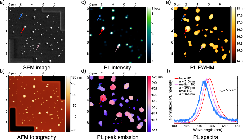
Figure 1a shows an SEM image of the sample with CsPbBr3 NCs and and FIB micro-markings used for the navigation across the sample and correlation of the obtained data. Here, we observe NCs of various shapes and sizes with the size distribution ranging from tens to hundreds of nm with the most frequent values peaking around 120 nm. The SEM image is accompanied by the AFM topography image (Figure 1b) of the identical sample area which displays the height distribution of the NCs ranging from 101 to 102 nm. Both SEM and AFM images are utilized to determine the aspect ratio and the volume of NCs, based on the characteristic width and height which are measured by SEM and AFM, respectively.
The morphology is correlated with PL maps in Figures 1c–e. The PL maps were obtained by COS – every pixel of the PL map has an assigned PL spectrum – and subsequent regression analysis of the PL spectra (see Methods). In Figure 1c we see the PL intensity map which matches the positions of the CsPbBr3 NCs visible in Figures 1a and b. By comparing these images, it is evident that bigger NCs exhibit brighter PL. Figure 1d displays the PL peak emission wavelength of the NCs ranging from 514 nm (2.41 eV) for the smaller NCs to 523 nm (2.37 eV) for the bigger NCs. The PL FWHM map (Figure 1e) shows the values ranging from 14 nm (68 meV) for smaller NCs to 18 nm (80 meV) for the bigger ones. Thanks to the correlation of structural Figure 1a,b and optical maps Figure 1c,d,e, we were able to assign particular PL spectra to individual CsPbBr3 NCs (Figure 1f).
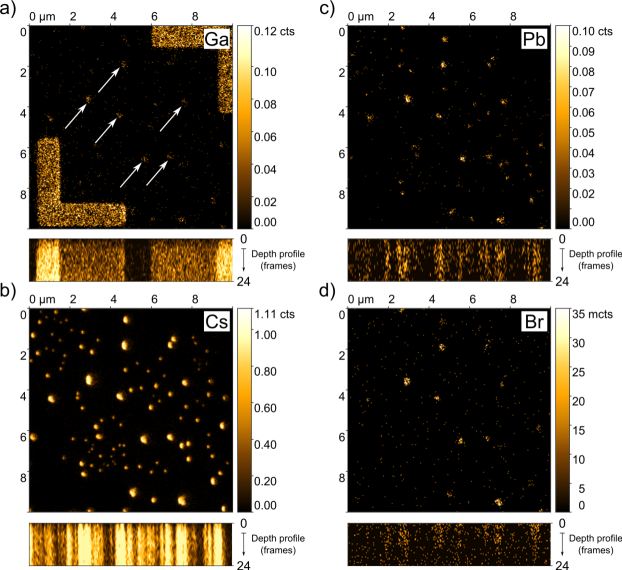
To exclude the role of local stoichiometry on the variance of PL properties of individual NCs, correlative elemental imaging by ToF-SIMS was performed. In Figure 2a–d, an analysed area is shown (the same as in Figure 1) to which are correlated the 3D spatial distributions of the detectable elements: Ga, Cs, Pb and Br ions acquired via ToF-SIMS analysis. Since Ga ion beam was used for both FIB micro-marking and ToF-SIMS elemental imaging, it is expected that the Ga ions will be present on the sample surface. From Figure 2a it seems, that some Ga ions were implanted also inside CsPbBr3 NCs (see the white arrows in Figure 2a). The fabrication of FIB micro-markings could in principle lead to the alteration of structural and optical properties of the examined samples. The influence of Ga ions implanted during the fabrication of FIB micro-markings on the optical properties of CsPbBr3 NCs was studied as follows. The PL response of several NCs was measured before and after their exposure to gallium ions used for the fabrication of the FIB markings. We discovered that the exposure to Ga ions of applied dose decreases the PL integral intensity by about 6 % but does not alter the PL peak emission wavelength or FWHM (see Supporting information, section S2). Figures 2b–d demonstrate the identical distribution of Cs, Pb, and Br elements throughout the whole volume of the sample. Further, integral XPS analysis points to high chemical purity of the NCs with stoichiometry Cs1.2Pb1Br2.8 (see Supporting information, section S3). These indicate that variations observed in the PL peak emission wavelength might be rather attributed to the morphology differences of the individual NCs and the related QCE.
To determine the dependency of the CsPbBr3 NCs’ PL response on their morphology, we have applied the quantum confinement effect (QCE) model based on the effective mass theory and parameters obtained by density functional theory (DFT) (see Methods and Supporting information, section S1). For the purpose of the simulations, we have proposed a model shape of NCs as a spheroid with only two parameters: the volume and the aspect ratio. Even though this shape does not fully correspond to the real image of the CsPbBr3 NCs, it respects the real aspect ratios. We were able to obtain the aspect ratio , where is the length of the NCs (Figure 1a) and is the height of the NCs (Figure 1b) from the CsPbBr3 NCs’ morphology. In Figure 3a, the histogram of the aspect ratios of individual NCs with values ranging from 1 to 4 is shown, with the values being the most common. This means that the lateral dimensions of the CsPbBr3 NCs tend to be larger than the vertical dimensions. The total volume of a such spheroid is then calculated as .
Let us consider an infinite potential well with the shape of a spheroid representing a single CsPbBr3 NC. The energy level distribution for an exciton confined within this system can be expressed as
| (4) |
where eV is the band gap of CsPbBr3, is the reduced effective exciton mass (see Supporting information, section S1 for values of the parameters), meV is the binding energy of an exciton accounting for the Coulomb interaction between an electron and a hole (see Methods), is the root of the Bessel function of the first kind where , , and as described in Ref. 62. The experimentally and theoretically retrieved values for the PL peak emission energy of individual NCs are plotted and compared as a function of a spheroid volume with a varying aspect ratio in Figure 3b. The theoretical values are systematically somewhat larger then the experimental ones. A plausible explanation is that the effective dimensions of NCs are smaller than the dimensions determined from the SEM and AFM images. Indeed, the wave function needs to vary smoothly in space. In the realistic NCs of irregular shape, the wave function cannot exploit the full volume of the particle. Instead, it approximately takes a spheroidal shape inscribed to the NC (see e.g. Fig. 4 in Ref. 63). Consequently, the effective dimensions of NCs are smaller. By analysis of the realistic particle shapes we estimate the difference of the effective and real dimension to be up to 25 % (see Supporting information S4). We show the corresponding theoretical dependences assuming the effective dimensions of NCs by the dashed lines in Figure 3b. Now, most of the experimental points agree well with this corrected theoretical prediction. It is also notable, that the amplitude of the PL peak emission energy shift (meV nm) being smaller than the average PL FWHM ( meV/ nm) results in a uniform macroscopic optical response of the hereby presented statistical ensemble of CsPbBr3 NCs across the sample with the PL peak emission energy shift detected only by high-resolution optical imaging.
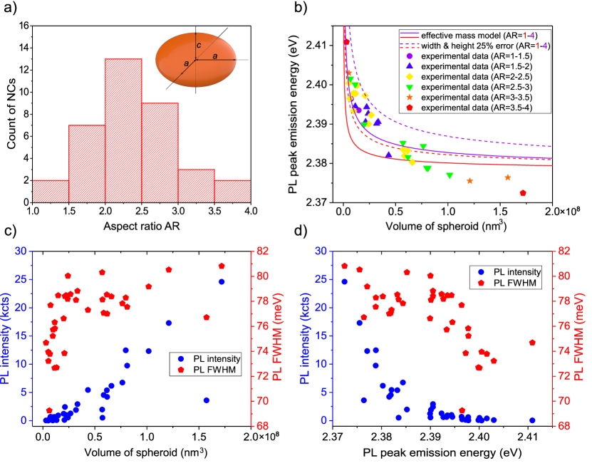
In Figure 3c a comparison is made between the experimentally determined PL intensity, PL FWHM, and NCs’ volume. Importantly, the PL intensity exhibits a linear dependence on the particle volume with 75 % of NCs having a deviation from the linear relationship bellow 20 % (blue points in Figure 3c). The effect of non-radiative processes, which could have significantly decreased the intensity of small particles on the surface, is insignificant. Notably, only 11 % of the particles show a considerably lower PL intensity, which can be attributed to structural defects, lattice strain, presence of the trap states or other non-radiative recombination channels 64, 65. Consequently, the total emission intensity is primarily linked to the volume of the material, indicating that the grain size does not have a significant impact. In Figure 3d, a comparison is made between experimentally determined PL intensity, PL FWHM, and PL peak emission energy. The PL intensity significantly decreases with the increasing PL peak emission energy. The FWHM of the emission exhibits a slight but systematic increase for larger particles. At present, the origin of this effect is unknown to us. We note that for very small particles (several units of nm) the opposite trend has been observed previously and attributed to the size dependence of the phonon-exciton coupling strength 35.
4 Conclusions
In conclusion, we have performed a comprehensive analysis of CsPbBr3 NCs at an individual NC level. It consisted of correlative high-resolution morphological and optical analysis which has been used to determine the relation between the shape and dimensions of NCs and their PL peak emission energy. These experimental results have been used as input to a simplified QCE model based on the effective mass approach. We have been able to successfully predict the PL peak emission energy for CsPbBr3 NCs based on the model of an exciton confined within the infinite spheroidal potential well. Our correlative analysis of a large statistical ensemble of individual CsPbBr3 NCs has the following implications for their utilization in various optoelectronic applications: (i) CsPbBr3 NCs produced by the simple drop-casting method are of high quality, exhibiting bright and size-tunable PL emission. (ii) The simplified and aspect ratio-based QCE model with effective masses obtained from DFT calculations qualitatively agrees with observed PL peak emission energies of CsPbBr3 NCs without the need for complex numerical simulations. Despite relatively big variations in the shape and size of individual NCs, the observed QCE is moderate, up to 9 nm in the wavelength. This is considerably smaller than their average PL FWHM, thus being detectable only by high-resolution PL mapping. (iii) The PL intensity exhibits a linear dependence on the particle volume and thus the total PL emission intensity of the NCs is primarily linked to the volume of the material, indicating that the grain size does not have a significant impact. (iv) CsPbBr3 NCs are compatible with the FIB processing with Ga ions, which poses an opportunity for precise nanoprocessing of individual NCs, as well as their integration into more complex devices including optical cavities or waveguides.
The authors acknowledge support by Czech Science Foundation, grant No. 19-06621S, Ministry of Education, Youth, and Sports of the Czech Republic (projects CzechNanoLab, No. LM2018110, Quality Internal Grants of BUT, No. CZ.02.2.69/0.0/0.0/19 073/0016948, sub-grant CEITEC VUT-K-22-7680), and Specific Research of BUT FCH/FSI-J-21-7396. The authors acknowledge Prof. Maksym Kovalenko’s laboratory for providing some perovskite mixtures used in this work.
The Supporting information is available.
References
- Morozov et al. 2017 Morozov, Y. V.; Zhang, S.; Brennan, M. C.; Janko, B.; Kuno, M. Photoluminescence Up-Conversion in CsPbBr3 Nanocrystals. ACS Energy Letters 2017, 2, 2514–2515
- Kovalenko et al. 2017 Kovalenko, M. V.; Protesescu, L.; Bodnarchuk, M. I. Properties and potential optoelectronic applications of lead halide perovskite nanocrystals. Science 2017, 358, 745–750
- Liu et al. 2017 Liu, F.; Zhang, Y.; Ding, C.; Kobayashi, S.; Izuishi, T.; Nakazawa, N.; Toyoda, T.; Ohta, T.; Hayase, S.; Minemoto, T. et al. Highly Luminescent Phase-Stable CsPbI 3 Perovskite Quantum Dots Achieving Near 100% Absolute Photoluminescence Quantum Yield. ACS Nano 2017, 11, 10373–10383
- Tong et al. 2016 Tong, Y.; Bladt, E.; Aygüler, M. F.; Manzi, A.; Milowska, K. Z.; Hintermayr, V. A.; Docampo, P.; Bals, S.; Urban, A. S.; Polavarapu, L. et al. Highly Luminescent Cesium Lead Halide Perovskite Nanocrystals with Tunable Composition and Thickness by Ultrasonication. Angewandte Chemie International Edition 2016, 55, 13887–13892
- Le et al. 2018 Le, Q. V.; Jang, H. W.; Kim, S. Y. Recent Advances toward High-Efficiency Halide Perovskite Light-Emitting Diodes. Small Methods 2018, 2
- Rainò et al. 2022 Rainò, G.; Yazdani, N.; Boehme, S. C.; Kober-Czerny, M.; Zhu, C.; Krieg, F.; Rossell, M. D.; Erni, R.; Wood, V.; Infante, I. et al. Ultra-narrow room-temperature emission from single CsPbBr3 perovskite quantum dots. Nature Communications 2022, 13, 2587
- Pan et al. 2015 Pan, J.; Sarmah, S. P.; Murali, B.; Dursun, I.; Peng, W.; Parida, M. R.; Liu, J.; Sinatra, L.; Alyami, N.; Zhao, C. et al. Air-Stable Surface-Passivated Perovskite Quantum Dots for Ultra-Robust, Single- and Two-Photon-Induced Amplified Spontaneous Emission. The Journal of Physical Chemistry Letters 2015, 6, 5027–5033
- Akkerman et al. 2018 Akkerman, Q. A.; Rainò, G.; Kovalenko, M. V.; Manna, L. Genesis, challenges and opportunities for colloidal lead halide perovskite nanocrystals. Nature Materials 2018, 17, 394–405
- Wang et al. 2016 Wang, Y.; Li, X.; Zhao, X.; Xiao, L.; Zeng, H.; Sun, H. Nonlinear Absorption and Low-Threshold Multiphoton Pumped Stimulated Emission from All-Inorganic Perovskite Nanocrystals. Nano Letters 2016, 16, 448–453
- Cheng et al. 2019 Cheng, L.-P.; Huang, J.-S.; Shen, Y.; Li, G.-P.; Liu, X.-K.; Li, W.; Wang, Y.-H.; Li, Y.-Q.; Jiang, Y.; Gao, F. et al. Efficient CsPbBr3 Perovskite Light-Emitting Diodes Enabled by Synergetic Morphology Control. Advanced Optical Materials 2019, 7
- Liu et al. 2021 Liu, M.; Wan, Q.; Wang, H.; Carulli, F.; Sun, X.; Zheng, W.; Kong, L.; Zhang, Q.; Zhang, C.; Zhang, Q. et al. Suppression of temperature quenching in perovskite nanocrystals for efficient and thermally stable light-emitting diodes. Nature Photonics 2021,
- Zhu et al. 2022 Zhu, C.; Marczak, M.; Feld, L.; Boehme, S. C.; Bernasconi, C.; Moskalenko, A.; Cherniukh, I.; Dirin, D.; Bodnarchuk, M. I.; Kovalenko, M. V. et al. Room-Temperature, Highly Pure Single-Photon Sources from All-Inorganic Lead Halide Perovskite Quantum Dots. Nano Letters 2022, 22, 3751–3760
- Jena et al. 2019 Jena, A. K.; Kulkarni, A.; Miyasaka, T. Halide Perovskite Photovoltaics. Chemical Reviews 2019, 119, 3036–3103
- Tong et al. 2020 Tong, G.; Ono, L. K.; Qi, Y. Recent Progress of All-Bromide Inorganic Perovskite Solar Cells. Energy Technology 2020, 8
- Duan et al. 2021 Duan, J.; Wang, M.; Wang, Y.; Zhang, J.; Guo, Q.; Zhang, Q.; Duan, Y.; Tang, Q. Effect of Side-Group-Regulated Dipolar Passivating Molecules on CsPbBr3 Perovskite Solar Cells. ACS Energy Letters 2021, 6, 2336–2342
- He et al. 2021 He, Y.; Petryk, M.; Liu, Z.; Chica, D. G.; Hadar, I.; Leak, C.; Ke, W.; Spanopoulos, I.; Lin, W.; Chung, D. Y. et al. CsPbBr3 perovskite detectors with 1.4% energy resolution for high-energy -rays. Nature Photonics 2021, 15, 36–42
- Xu et al. 2017 Xu, Y.-F.; Yang, M.-Z.; Chen, B.-X.; Wang, X.-D.; Chen, H.-Y.; Kuang, D.-B.; Su, C.-Y. A CsPbBr3 Perovskite Quantum Dot/Graphene Oxide Composite for Photocatalytic CO 2 Reduction. Journal of the American Chemical Society 2017, 139, 5660–5663
- Ko et al. 2021 Ko, J.; Ma, K.; Joung, J. F.; Park, S.; Bang, J. Ligand-Assisted Direct Photolithography of Perovskite Nanocrystals Encapsulated with Multifunctional Polymer Ligands for Stable, Full-Colored, High-Resolution Displays. Nano Letters 2021, 21, 2288–2295
- Qiu et al. 2018 Qiu, W.; Xiao, Z.; Roh, K.; Noel, N. K.; Shapiro, A.; Heremans, P.; Rand, B. P. Mixed Lead–Tin Halide Perovskites for Efficient and Wavelength-Tunable Near-Infrared Light-Emitting Diodes. Advanced Materials 2018, 31
- John et al. 2022 John, R. A.; Demirağ, Y.; Shynkarenko, Y.; Berezovska, Y.; Ohannessian, N.; Payvand, M.; Zeng, P.; Bodnarchuk, M. I.; Krumeich, F.; Kara, G. et al. Reconfigurable halide perovskite nanocrystal memristors for neuromorphic computing. Nature Communications 2022, 13, 2074
- Ma et al. 2021 Ma, W.; Jiang, T.; Yang, Z.; Zhang, H.; Su, Y.; Chen, Z.; Chen, X.; Ma, Y.; Zhu, W.; Yu, X. et al. Highly Resolved and Robust Dynamic X-Ray Imaging Using Perovskite Glass-Ceramic Scintillator with Reduced Light Scattering. Advanced Science 2021, 8, 2003728
- Xu et al. 2020 Xu, Q.; Wang, J.; Shao, W.; Ouyang, X.; Wang, X.; Zhang, X.; Guo, Y.; Ouyang, X. A solution-processed zero-dimensional all-inorganic perovskite scintillator for high resolution gamma-ray spectroscopy detection. Nanoscale 2020, 12, 9727–9732
- Heo et al. 2018 Heo, J. H.; Shin, D. H.; Park, J. K.; Kim, D. H.; Lee, S. J.; Im, S. H. High-Performance Next-Generation Perovskite Nanocrystal Scintillator for Nondestructive X-Ray Imaging. Advanced Materials 2018, 30, 2003728
- Fan et al. 2021 Fan, Y.; Tonkaev, P.; Wang, Y.; Song, Q.; Han, J.; Makarov, S. V.; Kivshar, Y.; Xiao, S. Enhanced Multiphoton Processes in Perovskite Metasurfaces. Nano Letters 2021, 21, 7191–7197
- Becker et al. 2018 Becker, M. A.; Vaxenburg, R.; Nedelcu, G.; Sercel, P. C.; Shabaev, A.; Mehl, M. J.; Michopoulos, J. G.; Lambrakos, S. G.; Bernstein, N.; Lyons, J. L. et al. Bright triplet excitons in caesium lead halide perovskites. Nature 2018, 553, 189–193
- Tamarat et al. 2023 Tamarat, P.; Prin, E.; Berezovska, Y.; Moskalenko, A.; Nguyen, T. P. T.; Xia, C.; Hou, L.; Trebbia, J.-B.; Zacharias, M.; Pedesseau, L. et al. Universal scaling laws for charge-carrier interactions with quantum confinement in lead-halide perovskites. Nature Communications 2023, 14, 229
- Zhang et al. 2015 Zhang, F.; Zhong, H.; Chen, C.; gang Wu, X.; Hu, X.; Huang, H.; Han, J.; Zou, B.; Dong, Y. Brightly Luminescent and Color-Tunable Colloidal CH 3 NH 3 PbX 3 (X = Br, I, Cl) Quantum Dots. ACS Nano 2015, 9, 4533–4542
- Xue et al. 2020 Xue, J.; Wang, R.; Yang, Y. The surface of halide perovskites from nano to bulk. Nature Reviews Materials 2020, 5, 809–827
- Luo et al. 2019 Luo, X.; Lai, R.; Li, Y.; Han, Y.; Liang, G.; Liu, X.; Ding, T.; Wang, J.; Wu, K. Triplet Energy Transfer from CsPbBr3 Nanocrystals Enabled by Quantum Confinement. Journal of the American Chemical Society 2019, 141, 4186–4190
- Abdi-Jalebi et al. 2018 Abdi-Jalebi, M.; Andaji-Garmaroudi, Z.; Cacovich, S.; Stavrakas, C.; Philippe, B.; Richter, J. M.; Alsari, M.; Booker, E. P.; Hutter, E. M.; Pearson, A. J. et al. Maximizing and stabilizing luminescence from halide perovskites with potassium passivation. Nature 2018, 555, 497–501
- Wei and Huang 2019 Wei, H.; Huang, J. Halide lead perovskites for ionizing radiation detection. Nature Communications 2019, 10
- Sichert et al. 2015 Sichert, J. A.; Tong, Y.; Mutz, N.; Vollmer, M.; Fischer, S.; Milowska, K. Z.; Cortadella, R. G.; Nickel, B.; Cardenas-Daw, C.; Stolarczyk, J. K. et al. Quantum Size Effect in Organometal Halide Perovskite Nanoplatelets. Nano Letters 2015, 15, 6521–6527
- Li et al. 2018 Li, H.; Qian, Y.; Xing, X.; Zhu, J.; Huang, X.; Jing, Q.; Zhang, W.; Zhang, C.; Lu, Z. Enhancing Luminescence and Photostability of CsPbBr3 Nanocrystals via Surface Passivation with Silver Complex. The Journal of Physical Chemistry C 2018, 122, 12994–13000
- Lin et al. 2021 Lin, H.; Wei, Q.; Ng, K. W.; Dong, J.; Li, J.; Liu, W.; Yan, S.; Chen, S.; Xing, G.; Tang, X. et al. Stable and Efficient Blue-Emitting CsPbBr3 Nanoplatelets with Potassium Bromide Surface Passivation. Small 2021, 17, 2101359
- Cheng et al. 2020 Cheng, O. H.-C.; Qiao, T.; Sheldon, M.; Son, D. H. Size- and temperature-dependent photoluminescence spectra of strongly confined CsPbBr3 quantum dots. Nanoscale 2020, 12, 13113–13118
- Imran et al. 2016 Imran, M.; Stasio, F. D.; Dang, Z.; Canale, C.; Khan, A. H.; Shamsi, J.; Brescia, R.; Prato, M.; Manna, L. Colloidal Synthesis of Strongly Fluorescent CsPbBr 3 Nanowires with Width Tunable down to the Quantum Confinement Regime. Chemistry of Materials 2016, 28, 6450–6454
- Protesescu et al. 2015 Protesescu, L.; Yakunin, S.; Bodnarchuk, M. I.; Krieg, F.; Caputo, R.; Hendon, C. H.; Yang, R. X.; Walsh, A.; Kovalenko, M. V. Nanocrystals of Cesium Lead Halide Perovskites (CsPbX3 , X = Cl, Br, and I). Nano Letters 2015, 15, 3692–3696
- Shamsi et al. 2021 Shamsi, J.; Rainò, G.; Kovalenko, M. V.; Stranks, S. D. To nano or not to nano for bright halide perovskite emitters. Nature Nanotechnology 2021, 16, 1164–1168
- Steele et al. 2021 Steele, J. A.; Solano, E.; Jin, H.; Prakasam, V.; Braeckevelt, T.; Yuan, H.; Lin, Z.; Kloe, R.; Wang, Q.; Rogge, S. M. J. et al. Texture Formation in Polycrystalline Thin Films of All-Inorganic Lead Halide Perovskite. Advanced Materials 2021, 33
- Jiang et al. 2019 Jiang, Q.; Zhao, Y.; Zhang, X.; Yang, X.; Chen, Y.; Chu, Z.; Ye, Q.; Li, X.; Yin, Z.; You, J. Surface passivation of perovskite film for efficient solar cells. Nature Photonics 2019, 13, 460–466
- Yoshikawa et al. 2017 Yoshikawa, K.; Kawasaki, H.; Yoshida, W.; Irie, T.; Konishi, K.; Nakano, K.; Uto, T.; Adachi, D.; Kanematsu, M.; Uzu, H. et al. Silicon heterojunction solar cell with interdigitated back contacts for a photoconversion efficiency over 26%. Nature Energy 2017, 2
- Kirchartz et al. 2020 Kirchartz, T.; Márquez, J. A.; Stolterfoht, M.; Unold, T. Photoluminescence-Based Characterization of Halide Perovskites for Photovoltaics. Advanced Energy Materials 2020, 10
- Stasio et al. 2017-09-26 Stasio, F. D.; Christodoulou, S.; Huo, N.; Konstantatos, G. Near-Unity Photoluminescence Quantum Yield in CsPbBr3 Nanocrystal Solid-State Films via Postsynthesis Treatment with Lead Bromide. Chemistry of Materials 2017-09-26, 29, 7663–7667
- Zhou et al. 2021 Zhou, Y.; Yu, Y.; Zhang, Y.; Liu, X.; Yang, H.; Liang, X.; Xia, W.; Xiang, W. Highly Photoluminescent CsPbBr3 /CsPb2Br5 NCs@TEOS Nanocomposite in Light-Emitting Diodes. Inorganic Chemistry 2021, 60, 3814–3822
- Dey et al. 2018 Dey, A.; Rathod, P.; Kabra, D. Role of Localized States in Photoluminescence Dynamics of High Optical Gain CsPbBr 3 Nanocrystals. Advanced Optical Materials 2018, 6
- Zhang et al. 2015 Zhang, D.; Eaton, S. W.; Yu, Y.; Dou, L.; Yang, P. Solution-Phase Synthesis of Cesium Lead Halide Perovskite Nanowires. Journal of the American Chemical Society 2015, 137, 9230–9233
- Anni et al. 2021 Anni, M.; Cretí, A.; Giorgi, M. L. D.; Lomascolo, M. Local Morphology Effects on the Photoluminescence Properties of Thin CsPbBr3 Nanocrystal Films. Nanomaterials 2021, 11
- Butkus et al. 2017 Butkus, J.; Vashishtha, P.; Chen, K.; Gallaher, J. K.; Prasad, S. K. K.; Metin, D. Z.; Laufersky, G.; Gaston, N.; Halpert, J. E.; Hodgkiss, J. M. The Evolution of Quantum Confinement in CsPbBr3 Perovskite Nanocrystals. Chemistry of Materials 2017, 29, 3644–3652
- Luo et al. 2019 Luo, X.; Lai, R.; Li, Y.; Han, Y.; Liang, G.; Liu, X.; Ding, T.; Wang, J.; Wu, K. Triplet Energy Transfer from CsPbBr3 Nanocrystals Enabled by Quantum Confinement. Journal of the American Chemical Society 2019, 141, 4186–4190
- Cheng et al. 2020 Cheng, O. H.-C.; Qiao, T.; Sheldon, M.; Son, D. H. Size- and temperature-dependent photoluminescence spectra of strongly confined CsPbBr3 quantum dots. Nanoscale 2020, 12, 13113–13118
- Morozov et al. 2017 Morozov, Y. V.; Zhang, S.; Brennan, M. C.; Janko, B.; Kuno, M. Photoluminescence Up-Conversion in CsPbBr 3 Nanocrystals. ACS Energy Letters 2017, 2, 2514–2515
- Kresse and Hafner 1993 Kresse, G.; Hafner, J. Ab initio molecular dynamics for liquid metals. Physical Review B 1993, 47, 558–561
- Kresse et al. 1994 Kresse, G.; Furthmüller, J.; Hafner, J. Theory of the crystal structures of selenium and tellurium. Physical Review B 1994, 50, 13181–13185
- Kresse and Furthmüller 1996 Kresse, G.; Furthmüller, J. Efficiency of ab-initio total energy calculations for metals and semiconductors using a plane-wave basis set. Computational Materials Science 1996, 6, 15–50
- Kresse and Furthmüller 1996 Kresse, G.; Furthmüller, J. Efficient iterative schemes for ab initio total-energy calculations using a plane-wave basis set. Physical Review B 1996, 54, 11169–11186
- Kresse and Joubert 1999 Kresse, G.; Joubert, D. From ultrasoft pseudopotentials to the projector augmented-wave method. Physical Review B 1999, 59, 1758–1775
- Becke 1993 Becke, A. D. A new mixing of Hartree–Fock and local density-functional theories. The Journal of Chemical Physics 1993, 98, 1372–1377
- Pack and Monkhorst 1977 Pack, J. D.; Monkhorst, H. J. "Special points for Brillouin-zone integrations"—a reply. Physical Review B 1977, 16, 1748–1749
- Perdew et al. 2008 Perdew, J. P.; Ruzsinszky, A.; Csonka, G. I.; Vydrov, O. A.; Scuseria, G. E.; Constantin, L. A.; Zhou, X.; Burke, K. Restoring the Density-Gradient Expansion for Exchange in Solids and Surfaces. Physical Review Letters 2008, 100
- Krukau et al. 2006 Krukau, A. V.; Vydrov, O. A.; Izmaylov, A. F.; Scuseria, G. E. Influence of the exchange screening parameter on the performance of screened hybrid functionals. The Journal of Chemical Physics 2006, 125
- Wang et al. 2021 Wang, V.; Xu, N.; Liu, J.-C.; Tang, G.; Geng, W.-T. VASPKIT: A user-friendly interface facilitating high-throughput computing and analysis using VASP code. Computer Physics Communications 2021, 267, 108033
- Kereselidze et al. 2016 Kereselidze, T.; Tchelidze, T.; Nadareishvili, T.; Kezerashvili, R. Y. Energy spectra of a particle confined in a finite ellipsoidal shaped potential well. Physica E: Low-dimensional Systems and Nanostructures 2016, 81, 196–204
- Huo et al. 2014 Huo, Y. H.; Křápek, V.; Rastelli, A.; Schmidt, O. G. Volume dependence of excitonic fine structure splitting in geometrically similar quantum dots. Physical Review B 2014, 90
- Jones et al. 2019 Jones, T. W.; Osherov, A.; Alsari, M.; Sponseller, M.; Duck, B. C.; Jung, Y.-K.; Settens, C.; Niroui, F.; Brenes, R.; Stan, C. V. et al. Lattice strain causes non-radiative losses in halide perovskites. Energy & Environmental Science 2019, 12, 596–606
- Wang et al. 2020 Wang, J.; Zhang, J.; Zhou, Y.; Liu, H.; Xue, Q.; Li, X.; Chueh, C.-C.; Yip, H.-L.; Zhu, Z.; Jen, A. K. Y. Highly efficient all-inorganic perovskite solar cells with suppressed non-radiative recombination by a Lewis base. Nature Communications 2020, 11