Current address: ]Department of Physics, Lancaster University, Lancaster LA1 4YB, United Kingdom
Optomechanical coupling and damping of a carbon nanotube quantum dot
Abstract
Carbon nanotubes are excellent nano-electromechanical systems, combining high resonance frequency, low mass, and large zero-point motion. At cryogenic temperatures they display high mechanical quality factors. Equally they are outstanding single electron devices with well-known quantum levels and have been proposed for the implementation of charge or spin qubits. The integration of these devices into microwave optomechanical circuits is however hindered by a mismatch of scales, between typical microwave wavelengths, nanotube segment lengths, and nanotube deflections. As experimentally demonstrated recently in [Blien et al., Nat. Comm. 11, 1363 (2020)], coupling enhancement via the quantum capacitance allows to circumvent this restriction. Here we extend the discussion of this experiment. We present the subsystems of the device and their interactions in detail. An alternative approach to the optomechanical coupling is presented, allowing to estimate the mechanical zero point motion scale. Further, the mechanical damping is discussed, hinting at hitherto unknown interaction mechanisms.
I Introduction
Optomechanics Aspelmeyer et al. (2014) and its manifold branches allow the characterization and manipulation of both macroscopic and nanoscale mechanical systems. By now readily available techniques include, e. g., ground state cooling Chan et al. (2011); Teufel et al. (2011) and squeezing Lecocq et al. (2015) of nanomechanical states, displacement sensing at and beyond the standard quantum limit Teufel et al. (2009), or on chip optical data processing Metcalfe (2014). Optomechanical techniques and formalisms have been applied to a wide range of material systems, from single atoms in traps to macroscopic interferometer mirrors Aspelmeyer et al. (2014).
Suspended single-wall carbon nanotubes (SW-CNTs) as mechanical resonators have been shown to reach high quality factors of up to Hüttel et al. (2009a); Moser et al. (2014) in a cryogenic environment. At the same time, they are excellent quantum dots and clean electronic quantum mechanical model systems, and transport spectroscopy at millikelvin temperatures has led to a large number of topical publications Laird et al. (2015); Margańska et al. (2019); Schmid et al. (2020). The observation of strong coupling between single electron tunneling and the motion of the macromolecule Steele et al. (2009); Lassagne et al. (2009) has inititated a further field of research Hüttel et al. (2010); Häkkinen et al. (2015); Götz et al. (2018), as has the integration of carbon nanotubes into circuit cavity quantum electrodynamics experiments Viennot et al. (2015); Desjardins et al. (2017).
Regarding the combination of the two fields, experimental approaches for optomechanics with carbon nanotubes at optical / visible frequencies exist Stapfner et al. (2013); Zhang et al. (2014); Tavernarakis et al. (2018); Barnard et al. (2019). However, since the photon energy exceeds the typical energy range of trapped electronic quantum states at low temperature, excitonic states, or even the electronic band gap, they are fundamentally incompatible with Coulomb blockade experiments. Consequently, this frequency range needs to be excluded from consideration in all experiments where the electronic confinement within the nanotube plays a role.
The small dimensions of typical single electron devices prevent effective integration into microwave optomechanical systems via conventional mechanisms relying only on radiation pressure Aspelmeyer et al. (2014); Regal et al. (2008). This mismatch of scales, critical for quasi one-dimensional objects as compared to, e.g., nanomechanical drum resonators Teufel et al. (2011); Das et al. (2023), becomes immediately obvious when comparing the typical microwave wavelength and thereby resonator size, for , the typical length of a suspended carbon nanotube quantum dot , and the typical deflection of such a suspended nanotube .
Recently, we have shown that the large variation in quantum capacitance of a CNT in the Coulomb blockade regime enhances the optomechanical coupling by several orders of magnitude at suitable choice of a working point Blien et al. (2020). Using optomechanically induced (in)transparency Agarwal and Huang (2010); Weis et al. (2010), a single photon coupling of up to was measured. Here, we expand upon the data evaluation and discussion of Blien et al. (2020) and characterize a wide range of interactions in the device already partly presented there — between the mechanical resonator, the microwave resonator, and the quantum dot in the Coulomb blockade regime. Combining different types of measurements, we provide an extended model, which allows us to estimate, e.g., the zero point motion amplitude of the carbon nanotube, further discuss consistency of the resulting device parameters, and characterize the mechanical damping mechanisms.
II Device and measurement setup
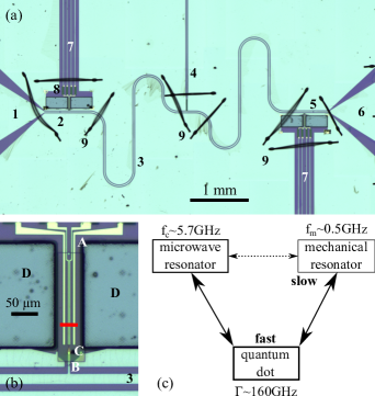
Our device, shown in Fig. 1(a), combines a superconducting coplanar microwave cavity with a suspended CNT quantum dot, this way acting as optomechanical hybrid structure. Coupling between the two subsystems is mediated via a gate electrode. This gate electrode, buried below the nanotube, is connected to the center conductor of the microwave resonator close to its input coupling capacitance, i.e., at one of the electric field and voltage antinodes.
Carbon nanotube and coplanar waveguide resonator form separate circuits, coupling to each other only capacitively. The CNT displays Coulomb blockade oscillations of conductance as function of gate voltage, but also acts as a high- mechanical oscillator. Initially, the CNT is characterized via standard low-frequency quantum dot transport spectroscopy Kouwenhoven et al. (1997); Laird et al. (2015), and the resonator via a GHz transmission measurement.
II.1 Niobium coplanar resonator
The microwave-optical subsystem of our device is given by a coplanar half-wavelength resonator Pozar (2012); Simons (2001); Gevorgian et al. (1995). On a high-resistivity () float-zone silicon substrate with a 500 nm thermally grown surface oxide, a uniform niobium layer is sputter-deposited. Using standard optical lithography followed by reactive ion etching, an impedance-matched coplanar waveguide (CPW) with in/out couple bond pads at both ends for transmission measurement is defined, see Fig. 1(a). Its center conductor 3 is interrupted by gaps twice, see 2 and 5 in Fig. 1(a), forming a type resonant cavity for transmission measurement. The gap width determines the coupling capacitances and across which the resonator is driven and read out; the distance between the gaps defines the resonator length and with it on first order the fundamental resonance frequency.
Close to the coupling capacitances, i.e., at the voltage antinodes, a stub-like extension of the center conductor connects to the gate electrode for the carbon nanotube, see B in Fig. 1(b) and the discussion below. Additionally, at its midpoint, i.e., the voltage node of the fundamental electromagnetic resonance mode, the center conductor is connected to a dc feed, 4 in Fig. 1(a), for the application of a gate bias Petersson et al. (2012). This dc feed, similar to the connections to the carbon nanotube discussed below, contains a thin, resistive gold meander with an approximate length of 3 mm acting as radio-frequency block.
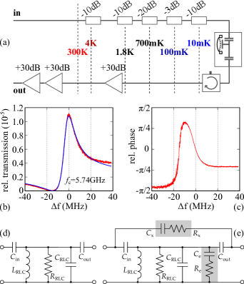
Figure 2(a) schematically shows the cryogenic measurement setup, Fig. 2(b) an example transmission measurement of the resonator at base temperature of the dilution refrigerator, and Fig. 2(c) the corresponding transmission phase. The measured value includes cable damping of approximately , the attenuators of distributed over the stages of the dilution refrigerator for input cable thermalization, a low temperature HEMT amplifier at the 1.8 K stage with amplification of , and a room temperature amplifier chain with a total amplification of approximately .
| Microwave cavity | |||
|---|---|---|---|
| Cavity resonance frequency | (1) | ||
| Cavity line width | (1) | ||
| Cavity quality factor | |||
| Cavity total capacitance | (2) | ||
| Replacement capacitance | |||
| Replacement inductance |
Any coplanar waveguide resonator can be translated into a lumped element RLC replacement circuit with identical resonant frequency Göppl et al. (2008). Fig. 2(d) displays the simplest such variant for a resonator measured in transmission Göppl et al. (2008). The relationship (for the fundamental resonance only) effectively expresses that fields are not distributed equally along the CPW cavity, with an electric field node of this mode at its center.
Our measurement displays a clear Fano shape instead of the Lorentzian naively expected from the circuit of Fig. 2(d), indicating the presence of additional non-resonant transmission channels parallel to the coplanar resonator. In terms of a circuit model, such a Fano shape can be taken into account by introducing a parallel channel Hornibrook et al. (2012), see Fig. 2(e) and in particular and there. In addition, the figure introduces the impact of a coupled carbon nanotube and its electrodes, via and .
Comparisons have however shown that it makes no significant difference for our evaluation whether we calculate the parameter for Fig. 2(e) analytically or work with a conceptually much simpler Fano model that absorbs and into and and takes and into account via a complex constant offset of . In this model one obtains for the transmission Khalil et al. (2012); Petersan and Anlage (1998)
| (1) |
where and describe transmission amplitude and phase of the parallel, parasitic channel. Using a fit of Eq. (1), we obtain from the measurement a resonance frequency and a resonance width of , corresponding to a quality factor . Table 1 collects these device parameters as an overview.
In comparison with similar experiments from literature Regal et al. (2008); Singh et al. (2014), the observed quality factor of our device is surprisingly low. Given that we have already fabricated coplanar waveguide resonators with intrinsic quality factors of Blien et al. (2016), the limitation is likely not given by resonator or substrate material or the resonator patterning process per se. Two factors contribute here. On the one hand, the multiple lithographic steps required for device fabrication lead to an increased chance of defects and contamination. Examples can be seen in Fig. 1(a) near the center of the coplanar waveguide resonator, with veil-like structures from fluorinated resist residues. Testing of multiple resonator devices has shown that such structures on top of the center conductor lead to a significant decrease of the quality factor.
On the other hand, the dc electrodes of the carbon nanotube deposition areas couple out part of the GHz signal from the coplanar resonator. While the gold meanders in the dc connections are intended as inductive high-frequency blocks, they are also resistive, leading to signal dissipation. Future device design shall replace them with reflective low-pass filters Hao et al. (2014) to avoid signal loss near the cavity resonance.
II.2 Carbon nanotube quantum dot
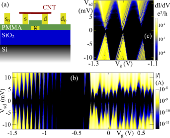
The device includes two regions where a carbon nanotube can be deposited onto contacts next to the coplanar waveguide resonator, see Fig. 1(b). For the measurements presented here, only one of these was used. The detailed carbon nanotube growth and transfer procedure, adapted from works of other research groups in the field, has already been discussed in detail elsewhere Wu et al. (2010); Blien et al. (2018, 2020). After deposition, the nanotube freely crosses a trench of width between two gold electrodes acting as source and drain. A finger gate at the bottom of the trench, below an isolating PMMA layer, is connected to the coplanar waveguide resonator for coupling, and can also be used to apply a dc gate voltage, see Fig. 3(a).
When varying the applied gate voltage, we observe the typical Coulomb blockade oscillations of a quantum dot Kouwenhoven et al. (1997); Tans et al. (1997); Laird et al. (2015), see Fig. 3(b). In this overview plot of the dc current, , an apparent electronic band gap around is flanked on both sides by Coulomb blockade oscillations. A detail measurement of the differential conductance in the parameter region later used for the optomechanical measurements, Fig. 3(c), displays multiple differential conductance lines in single electron tunneling, possibly related to longitudinal vibration Braig and Flensberg (2003); Koch and von Oppen (2005); Sapmaz et al. (2006); Hüttel et al. (2009b); Stiller et al. (2020), electronic excitations, or trap states in the contacts. No clear fourfold shell pattern of the Coulomb oscillations can be observed, possibly due to small-scale defects or disorder of the CNT.
| Nanotube quantum dot | |||
|---|---|---|---|
| Gate capacitance | (1) | 2.6 aF | |
| Total capacitance | (1) | 9.8 aF | |
| Gate lever arm | 0.27 | ||
| Total tunnel rate | (1) | 160 GHz | |
| Effective electronic length | |||
| Nanotube mechan. resonator | |||
| Mode 1 curvature | (2) | ||
| Mode 1 center voltage | (2) | ||
| Mode 1 center frequency | (2) | ||
| Mode 2 curvature | (2) | ||
| Mode 2 center voltage | (2) | ||
| Mode 2 center frequency | (2) | ||
| Normal mode splitting 1-2 | (2) | ||
| Suspended length of nanotube | (3) | ||
| Radius of nanotube | (4) | ||
| Effective mass | (4) | ||
| Imprinted tension | (5) | ||
| Mech. line width | |||
| Quality factor |
In the parameter region discussed in detail below we obtain via evaluation of the Coulomb blockade data of Fig. 3(b,c) Kouwenhoven et al. (1997) for the quantum dot capacitances of and , and with these the gate conversion factor , see also Table 2. In addition, we can estimate the total tunnel rate of quantum dot–lead coupling from the zero-bias conductance peak broadening. A value of , corresponding to , is consistent both with conductance and (as discussed later) optomechanical coupling Blien et al. (2020). This makes electronic tunneling the fastest relevant time scale in our coupled system, cf. Fig. 1(c), clearly exceeding the cavity and mechanical resonance frequencies.
An estimation of the gate capacitance via a simple wire-over-plane model Blien et al. (2020); Wunnicke (2006), using an averaged relative dielectric constant and a gate distance , coincides with the gate capacitance from Coulomb blockade for a reduced length of the nanotube; we call this the effective electronic length of our carbon nanotube quantum dot. This models, e.g., the reduction caused by depletion regions in pn-barriers, or more generally corrects for geometry deviations.
II.3 Driven vibrational motion of the nanotube
The behavior of a carbon nanotube quantum dot as high- nanomechanical resonator at cryogenic temperatures has been discussed in many recent works Hüttel et al. (2009a); Steele et al. (2009); Moser et al. (2014); Häkkinen et al. (2015); Schmid et al. (2015); Götz et al. (2018); Rechnitz et al. (2022). The dominant external force acting on the nanotube as a suspended beam is given by the electrostatic force of the gate charge acting on the quantum dot charge; the restoring force stems from the tension, either built-in or deflection induced, and the bending rigidity of the macromolecule. Overall deflection leads to an elongation, increase of the tension, and thereby an increase of its mechanical resonance frequency Sazonova et al. (2004); Witkamp et al. (2006).
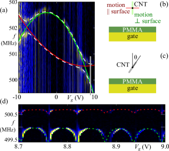
The fundamental bending mode resonance frequency of a suspended nanotube scales with the segment length as ; from literature we typically expect it in the range of for a long nanotube Sazonova et al. (2004); Witkamp et al. (2006); Hüttel et al. (2009a); Schmid et al. (2012); Götz et al. (2019). The device presented here shows two resonances around , see Fig. 4(a). In the plot, a lock-in amplifier is used to amplitude-modulate the applied rf driving signal at and pick up the corresponding modulation of the low-frequency current through the nanotube; while slightly less sensitive than the so-called frequency modulation technique Gouttenoire et al. (2010), this method retains a more natural resonance shape.
A thorough search at lower drive frequencies led to no additional results. In combination with the weak gate voltage dependence, this indicates a high built-in tension imprinted onto the carbon nanotube during fabrication. Its origin likely lies in the transfer of carbon nanotubes into the resonator circuit Wu et al. (2010); Blien et al. (2018, 2020). The nanotubes are grown on a quartz fork and lowered onto the contact electrodes until a finite current is measured. Then, they are locally cut by resistive heating with a large current through it. The heating only affects the nanotube and its immediate surroundings, with the macromolecule slightly melting the gold contacts and attaching there; traces of this have been observed in microscope images of test structures. The force pulling the nanotube over the contacts leads to an eventual imprinted tension in the device.
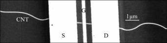
This effect is also illustrated by the SEM image of Fig. 5. It shows a different, subsequently produced device, where however similar fabrication steps and lithographic geometries have been used. Between source (S) and drain (D) electrode, the visible nanotube (CNT) is stretched straight, while it is clearly non-tensioned outside these electrodes.
Cooling of the device from room temperature to base temperature of the dilution refrigerator leads to a thermal contraction of the silicon substrate. Even though a negative axial coefficient of expansion for carbon nanotubes has been theoretically predicted for a long time Kwon et al. (2004); Mounet and Marzari (2005); Balandin (2011), surprisingly few experiments exist Chi et al. (2018). What data there is confirms a negative thermal expansion, hinting that the cooling of the nanotube and the expansion coefficient mismatch with the substrate should not introduce tension (but rather counteract tension or induce buckling).
Our observed modes in the tensioned case correspond in first approximation to the fundamental transversal vibration parallel to the device surface and towards the gate Kozinsky et al. (2006), see Fig. 4(b): only for the latter, electrodynamic softening of the vibration mode Kozinsky et al. (2006); Wu and Zhong (2011); Stiller et al. (2013) contributes to the large-scale gate voltage dependence of the resonance frequency, inverting the dispersion at low gate voltage. The negative curvature term is absent for motion parallel to the chip surface, where only the tension-induced frequency increase is observed. Note that this model, treating the nanotube as a two-dimensional oscillator, still simplifies away many physically relevant details, from the deflection envelope along the nanotube all the way to screw-like motions or buckling Rechnitz et al. (2022).
As fit functions in Fig. 4(a), two coupled classical harmonic oscillator modes with general parabolic dispersion
| (2) |
are chosen (; solid lines in the figure), leading to fit functions
| (3) |
(dashed lines in the figure). Here, parametrizes the coupling between the two modes. In the evaluated voltage range, this model describes the large-scale gate voltage dependence of the resonance frequencies very well; the resulting fit parameters can be found in Table 2. The coupling of the vibration modes via the tension of the nanotube induces a sizeable mode splitting of , similar in magnitude to previous observations Eichler et al. (2012).
With the effective mass , , and the suspended length , we obtain using the relation
| (4) |
the remarkably large fabrication-imprinted tension (i.e., the axial tension of the nanotube in absence of electrostatic forces) .
Assuming now that the contributions to the spring constant add up linearly, we can use the difference in curvature of the two modes to isolate the electrostatic softening effects alone. With , following Eichler et al. (2011); Stiller et al. (2013)
| (5) |
we obtain . The wire-over-plane model, with the length of the wire rescaled as discussed above to the effective electronic length , leads to , approximately a factor 4 smaller.
While one may typically expect symmetric behaviour around Solanki et al. (2010), static charges e.g. at the substrate surface can explain a common offset of the extrema of both modes. This however provides no straightforward explanation for the relative shift of the two modes in , with the frequency maximum of the electrostatically softened mode at and the minimum of the non-softened mode at .
III Interaction of the subsystems
III.1 Microwave resonance shift due to Coulomb blockade
As already mentioned above, the effective replacement circuit capacitance (see Fig. 2(d)) is directly related to the geometric capacitance of the coplanar waveguide resonator, taking into account the spatial distribution of electric fields. For our resonator, we calculate a geometric capacitance of , neglecting the small and constant coupling capacitances. In the case of the fundamental mode of our resonator and its field distribution, this translates to Simons (2001). With the resonance frequency, we obtain a corresponding replacement circuit inductance , which is in the following assumed constant.
The gate voltage dependent contribution of the quantum dot to the total replacement circuit capacitance can be written as quantum capacitance
| (6) |
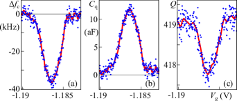
with the gate conversion factor of the quantum dot as introduced above. It describes the response of the gate charge to a gate voltage fluctuation Delbecq et al. (2011); Desjardins et al. (2017); Roschier et al. (2005). In Coulomb blockade, is effectively zero since the charge on the quantum dot is constant for small voltage variations. In contrast, a maximum of is reached at the position of a conductance peak where the charge on the quantum dot varies. This becomes directly visible as a reduction of the cavity resonance frequency .
A corresponding measurement is shown in Fig. 6(a). For each value of the gate voltage across a Coulomb oscillation, a trace of the coplanar waveguide resonator transmission has been recorded. Fitting the transmission data with Eq. (1), we obtain the resonance frequency and its change induced by the quantum capacitance, Fig. 6(a), and the resonator quality factor , Fig. 6(c). Assuming constant , we then translate into a change in replacement circuit capacitance , see Fig. 6(b). Remarkably, this effective value is larger than the bare geometric gate capacitance of the CNT to the gate finger .
The quality factor of the microwave resonator is clearly reduced when the nanotube quantum dot is in single electron conduction, see Figure 6(c). This effect is not covered by the circuit model, but can be explained as follows. As discussed below in Section III.3 in detail, we can estimate the voltage amplitude of the driven cavity and with it the energy stored in the cavity. Using the data of Fig. 9(b), we obtain for the parameters of Fig. 6 and . This ac voltage amplitude is consistent with the width of the Coulomb oscillation in Fig. 9(a), Section III.3, at a nominal generator drive power of .
The dip in the cavity -factor indicates an additional energy loss per microwave period induced by single electron tunneling. The loss can be estimated as
| (7) |
Applying a model initially developed for nanoelectromechanical systems Meerwaldt et al. (2012), we assume that due to the finite tunnel rate connecting the quantum dot to its leads the quantum dot occupation only follows the potential oscillation with a delay. This way, electrons are pumped from lower to higher energy states, resulting in an energy loss for the microwave resonator.
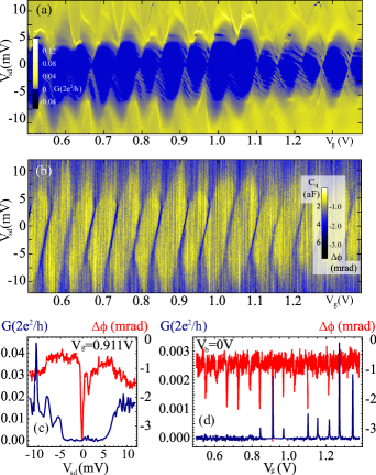
Figure 7 illustrates the mechanism as well as the expected average energy lost during one microwave period: an electron tunnels from the quantum dot to the electrodes on average after the time , extracting from the microwave resonator. The same amount of energy is extracted after the gate potential is below the SD energy. Coulomb blockade ensures that during one microwave cycle at most one electron undergoes this process. The combined tunnel rate of the contacts thus relates to as
| (8) |
For and the parameters given in the measurement of Fig. 6(c), we obtain a tunnel rate , in reasonable agreement with the previous estimate from Coulomb blockade for this parameter.
III.2 Transmission phase based quantum capacitance detection
At or close to the microwave cavity resonance , the transmission phase of the microwave resonator is highly sensitive to the drive frequency deviation , see Fig. 2(b). A slight shift of the resonance frequency, e.g., due to changes of the resonator environment, becomes equally visible as a transmission phase shift, with an approximate linear relation. This allows to efficiently probe the resonator and with it the quantum capacitance of the adjunct nanotube system, a technique that has already been applied successfully to carbon nanotubes, see Delbecq et al. (2011); Desjardins et al. (2017). Both the resonance shift (max. ) and the change in resonance width from (max. ) identified in Fig. 6 cannot move our working point significantly relative to the wide cavity resonance nor significantly change the slope of the linear relation. With and we obtain a phase shift of .
A corresponding measurement is shown in Fig. 8. Fig. 8(a) and Fig. 8(b) plot the simultaneously measured dc conductance and microwave transmission phase, as function of applied gate voltage and bias voltage , over a range of several Coulomb oscillations. Fig. 8(c) and Fig. 8(d) are trace cuts from the measurement, for (c) constant gate voltage and (d) constant bias voltage .
The Coulomb oscillations and with them the oscillatory behaviour of the quantum capacitance in are immediately visible. In Fig. 8 we use an input filter bandwidth of the VNA of , corresponding to an integration time per point on the order of . From the phase noise of the trace cut of Fig. 8(c) we can estimate a measurement sensitivity of or better, see also Desjardins et al. (2017). While this does not reach the resolution of Fig. 6(b), it is recorded significantly faster.
In Fig. 8(b), the phase shift highlights a preferred edge of the single electron tunneling regions as the parameter region where the time-averaged charge of the quantum dot changes by one electron. This indicates that the tunneling rates from the quantum dot to source and drain differ significantly; in single electron tunneling the time-averaged charge is close to one of the neighbouring Coulomb blockade regions. Charging of the quantum dot predominantly happens when the quantum dot potential crosses the Fermi edge of the contact with the higher tunneling rate. Similar observations have already been made on quantum dots with asymmetrically coupled reservoirs Schleser et al. (2005); Desjardins et al. (2017); for an in detail analysis of charging and tunnel rates see Schleser et al. (2005), where a quantum point contact charge detector is used to obtain an equivalent signal.
III.3 Impact of GHz signals on the quantum dot
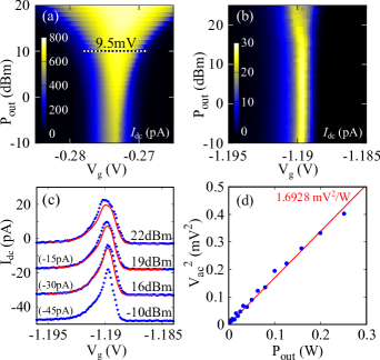
The impact of a microwave signal in the resonator on dc (or, more precisely, time-averaged / rectified) transport through the quantum dot, i.e., the reverse effect compared to above discussion, is shown in Fig. 9. Since the electronic tunnel rates and thus the Coulomb oscillation width GHz Blien et al. (2020) clearly exceed the drive frequency , we can treat the microwave signal as a classical oscillating gate voltage. In a first approximation, this signal, too fast for our low-frequency circuit to follow, thus effectively widens the observed Coulomb oscillations.
This is demonstrated in Fig. 9(a) for a resonant and in Fig. 9(b) for an off-resonant cavity drive. In Fig. 9(a), increasing additionally leads to a peak current increase, indicating that at the resulting large photon numbers in the cavity the approximation of broadening of the peak only breaks down. For the off-resonant case in Fig. 9(b), the peak current decreases with applied power, and we can model the impact of the ac signal numerically by averaging a (near) zero-drive gate trace over a sinusoidal gate voltage of given amplitude.
In detail, we extract a trace at small or zero drive amplitude (here, at ) and then numerically find the ac gate voltage amplitude such that the average
| (9) |
best fits to a measured trace at finite drive amplitude. Example results are shown in Fig. 9(c), for data measured at and the resulting best ac voltages for the broadening . The lowermost set of points shows the reference trace at . Fig. 9(d) plots the square of the ac voltage as function of generator power , demonstrating that these values are proportional as expected.
We approximate that due to the proximity of the nanotube transfer regions to the coupling capacitors of the coplanar waveguide resonator the ac gate voltage amplitude is equal to the voltage amplitude at the resonator antinode (i.e., at the coupling capacitor). This allows an estimate of the photon number in the resonator as function of applied drive power. Using the linear fit of Fig. 9(d) (red sideband drive) and the replacement circuit capacitance as discussed above, a generator drive power of translates to a voltage amplitude of and to resonator photons. A more detailed discussion of error sources for the estimation can be found in Appendix A.
Note that the measurements of Fig. 9(b-d) have been performed with an off-resonant drive of the cavity. In the case of a resonant drive, the increased photon occupation (larger by a factor of ) leads to a correspondingly stronger ac signal and thereby broadening, see Fig. 9(a). Calculating the expected peak width for at resonance gives , which is in good agreement with the observation in Fig. 9(a), see the scale bar in the figure. Additionally, the maximum current increases at large power, which is in clear disagreement with our simple broadening model. For tunneling through a single, discrete level in the quantum dot, heating of the electron gas in the contacts leads to a decrease of the current Beenakker (1991). This leaves as explanation for the increase either accessing excited states as additional transport channels via the broadened Fermi distribution of the contacts or more complex processes such as (multi-)photon-assisted tunneling.
III.4 Interaction of vibration and Coulomb blockade
Figure 4(d) shows a detail measurement of the driven mechanical resonances, corresponding to a zoom of the region marked in Fig. 4(a) with a gray bar. Here, the impact of the Coulomb oscillations on the two mechanical modes becomes clearly visible Steele et al. (2009). Comparison with Fig. 4(a) lets us conclude that the lower mode with is predominantly the globally softening (perpendicular to the device surface) mode and the upper mode with is predominantly the globally hardening (parallel to the device surface) mode. The measurement is still near the mode anticrossing at , however, such that a finite mode mixing cannot be excluded.
The dashed lines in Fig. 4(c) correspond to fits to the extracted resonance positions. We simplify the Coulomb oscillations as a sequence of 6 equidistant Lorentzians in conductance, with the corresponding increase of the time-averaged number of electrons in the quantum dot from the resonant tunneling picture. Since the oscillation at does not fit in to this equidistant peak scheme (which is not particularly surprising for a carbon nanotube quantum dot with significant quantum mechanical contributions to the addition energy), we ignore the data points around this one Coulomb oscillation. The overall fit function used for each of the two mechanical modes () is
| (10) |
where in particular captures the local electrostatic softening through the Coulomb blockade oscillation, expressed in Steele et al. (2009) for the spring constant as
| (11) |
(Eqn. (S5) there, with other control parameters such as constant).
For a vibration mode whose motion does not change the gate capacitance, no local capacitive softening is expected, and indeed the higher frequency mode in Fig. 4(c) shows a much smaller coupling to the Coulomb oscillations. From the fits, we obtain a ratio , leading to a ratio of the capacitance sensitivities , which would be fulfilled for two relatively perpendicular vibration modes both rotated by to the device surface normal. For future measurements it would be interesting to trace a mode anticrossing as in Fig. 4(a) in more detail and extract the evolution of the couplings and their ratio as function of gate voltage in this nano-electromechanical model system.
IV Quantum capacitance enhanced optomechanics
IV.1 Introduction
Dispersive coupling is both experimentally and theoretically the most widely researched mechanism for obtaining an optomechanical system Aspelmeyer et al. (2014). Here, mechanical displacement causes a change in resonance frequency of an electromagnetic / optical resonator. In a microwave optomechanical system, this typically happens via a modification of the capacitance of a -circuit; one of the capacitor electrodes is the mechanically active element.
While optomechanical effects in a combined nanotube–microwave resonator system as shown in Fig. 10(a) can in principle occur due to geometrical capacitance changes alone, a quick estimate already shows that the resulting coupling parameters are tiny Blien et al. (2020). Essentially, this is a manifestation of a mismatch of scales. Working frequencies for coplanar waveguide resonators are typically in the range . With this one obtains wavelengths and resonator sizes on the order of . A carbon nanotube segment with ballistic conduction, where electrons can be confined to single, well-separated and unperturbed quantum levels, has typically a length of . Mechanical deflections of such a segment as vibrational resonator are in the range of (at strong driving) Schmid et al. (2012) and (zero point motion) Blien et al. (2020). Obviously, a deflection will barely affect the geometric properties of a resonator of size .
In the following, the nonlinear charging characteristic of the quantum dot embedded in the nanotube is used for amplification of the coupling. As demonstrated above, it leads to a gate voltage dependent, locally strong quantum capacitance contribution, which can dominate geometric effects. The mechanical oscillation is slow compared to both tunnel rates and microwave resonance frequency, allowing us to treat this quantum capacitance as a replacement parameter which again depends on the deflection. At proper choice of the gate voltage working point, optomechanical experiments become possible Blien et al. (2020).
| Input signals | |||
|---|---|---|---|
| Drive generator power | |||
| Probe (VNA) power | |||
| estimated cable damping | |||
| Subsystems | |||
| Cavity resonance frequency | |||
| Cavity line width | |||
| Cavity quality factor | |||
| Mech. resonance frequency | |||
| Mech. line width | |||
| Mech. quality factor | |||
|
Coupling parameters
() |
|||
| Side band resolution | 43.5 | ||
| Single photon coupling | |||
| Optomechanical coupling | |||
| Cavity pull-in parameter | |||
| Dispersive coupling | |||
| Max. sideband cooling rate | |||
| Cooperativity | |||
| Cooling power |
IV.2 Optomechanically induced (in)transparency OMIT
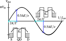
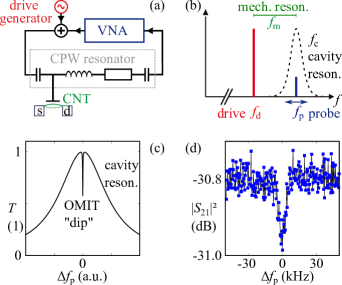
Our experiment for detecting and determining the optomechanical coupling is a so-called optomechanically induced transparency (“OMIT”) measurement, introduced first by Weis et al. Weis et al. (2010) and based on earlier work on electromagnetically induced transparency of resonator media Boller et al. (1991). Fig. 10(a) displays the simplified high frequency circuit, Fig. 10(b) schematically sketches the involved frequencies. A strong drive signal is applied at a constant frequency red-detuned from the cavity resonance by the mechanical resonance frequency, . Additionally a probe signal is swept across the cavity resonance and its transmission measured.
Extending Eq. (1), the transmission of the probe signal, proportional to the intracavity photon number, now follows the broad peak of the electromagnetic resonance everywhere except near , where a dip in transmission emerges, see also Fig. 10(c):
| (12) |
Here, is the optomechanical coupling for the total number of cavity photons , which is at fixed drive frequency proportional to the drive power. Microscopically Eq. (12) can be motivated such that mechanical phonons of frequency pair up with photons of , upconverting to the cavity frequency , and then interfere destructively with the probe signal at Weis et al. (2010), suppressing the population of the cavity.
The width of the optomechanically induced transmission dip in Eq. (12) is given by the effective mechanical damping rate Aspelmeyer et al. (2014),
| (13) |
where the latter term in the sum, see also Table 3,
| (14) |
is exactly the dispersive optomechanical damping (or cooling) rate induced by the red sideband detuned drive signal in absence of the weak probe signal.
IV.3 Quantum capacitance amplified coupling
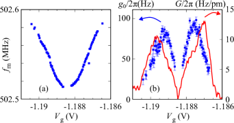
As visible from Eq. (12), the multi-photon optomechanical coupling as well as several other parameters can be extracted directly from OMIT measurements as curve fit parameters. This becomes particularly interesting when stepping the dc gate voltage across a Coulomb oscillation and plotting the parameters as function of gate voltage. Already well-known behaviour can be seen in Fig. 11(a), with the gate voltage dependence of the mechanical resonance frequency , now extracted from fits of Eq. (12) to OMIT data. The decrease of corresponds to the local electrostatic softening (or the “Coulomb oscillations of mechanical resonance frequency”) as also already demonstrated in Fig. 4(d) and in earlier publications Steele et al. (2009); Hüttel et al. (2010); Götz et al. (2018).
Using the cavity photon number as determined previously, see Fig. 9, the single photon optomechanical coupling can be calculated; it is plotted in Fig. 11(b) (blue points, left axis). The data clearly shows maxima on the flanks of the Coulomb oscillation, while the coupling both vanishes at its center and in Coulomb blockade. This behaviour has already been discussed in detail in Blien et al. (2020). There it was shown that is connected to the time-averaged number of electrons on the quantum dot , increasing by one over a Coulomb oscillation, via
| (15) |
Assuming a lifetime-broadened level in the quantum dot and thus a Lorentzian shape of , Eq. (15) allows to approximate the functional dependence of the data in Fig. 11(b) (points) very well. In quantitative terms, theory and experiment differ by approximately a factor 5, still an excellent agreement given the amount of approximations that enter the calculation Blien et al. (2020).
An alternative way to characterize the optomechanical coupling is directly via the cavity pull-in parameter , i.e., the cavity resonance frequency shift per mechanical displacement,
| (16) |
We can extract this parameter from the gate voltage dependence of the resonance frequency , Fig. 6(a), which directly provides us the quantum capacitance , Fig. 6(b). The details are given in Appendix B and lead to
| (17) |
where again is the geometric capacitance between resonator (gate) and nanotube (quantum dot), which can be extracted rather precisely from Coulomb blockade measurements, and is the quantum capacitance as plotted in Fig. 6(b).
The result for is plotted in Fig. 11(b) as a solid red line. An offset in gate voltage has been corrected here; it most likely was caused by charging effects over the course of the lengthy measurement cool-down. The functional dependence agrees well with the OMIT result. The Coulomb oscillation structure appears to be slightly wider in gate voltage for . Comparing the applied powers of the resonant probe signal in the OMIT case and the repeated cavity resonance sweeps of Fig. 6, , this effect is however well within the possible broadening of the Coulomb oscillation by the GHz signal.
Since the two parameters and are proportional and their proportionality factor is exactly the zero point fluctuation scale of the mechanical system, this provides us a way to estimate . Bringing the two curves in Fig. 11(b) to best agreement leads to . Using the harmonic oscillator expression with the effective mass as given in Table 2 and used otherwise in the calculations, we obtain ; again the values agree better than one order of magnitude.
Regarding error sources, for the cavity pull-in parameter , Eq. (17), all values can be directly read out from the measurement, with the exception of . The latter is calculated by scaling the wire-over-plane model for a gated carbon nanotube Blien et al. (2020); Wunnicke (2006) down to the effective electronic length of the nanotube quantum dot: we calculate the theoretical capacitance between suspended nanotube and gate from the device geometry, compare it with the Coulomb blockade derived gate capacitance to obtain an effective electronic length, and scale the theoretical derivative accordingly.
Conversely, the main error source for the single photon optomechanical coupling from Blien et al. (2020) is the cavity photon number , derived with the assumption that the gate electrode shows the same GHz voltage amplitude as the end of the coplanar waveguide resonator at its coupling capacitance (and voltage antinode). This error could be reduced by, e.g., more detailed finite element modeling of the device. However, since the exact position and orientation of the deposited carbon nanotube is unknown in the experiment, it is unclear whether the additional effort would be of much help.
IV.4 Damping of the motion in OMIT
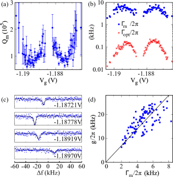
Figure 12(a) plots the mechanical quality factor extracted from OMIT via Eq. (12). displays two distinct minima on the Coulomb oscillation flanks, and on the whole a behaviour inverse to the optomechanical coupling . This is clearly different from damping induced by electronic tunneling alone, see, e.g., Meerwaldt et al. Meerwaldt et al. (2012), where for only a single minimum of the quality factor is observed.
The total, effective damping rate of the mechanical system taking into account optomechanical coupling is given by Eq. (13), combining mechanical behaviour and the damping via upconversion of the red-detuned drive signal. For comparison of scales, the extracted damping rate , inversely proportional to , varies in the range . At the same time, we find . This indicates that even at our enhanced optomechanical coupling the damping via upconversion from Eq. (13) is small in the experiment. Figure 12(b) plots both values as function of , confiming this conclusion with a nearly two orders of magnitude smaller optomechanical damping for any gate voltage.
An apparent variation in and the width of the OMIT dip can be caused by mechanically nonlinear behaviour. Equation (12) assumes a harmonic oscillator; if strong driving leads to a distortion of the mechanical resonance shape towards a Duffing curve, the fit will return artificially smaller values. Fig. 12(c) plots several raw data curves of the frequency-dependent power transmission as examples. While occasionally asymmetric curve shapes can be observed in the raw data with its scatter, no systematic gate voltage dependence of this nonlinear behaviour emerges. Thus, no conclusion about the impact of nonlinearity on the fit results can be made.
In Fig. 12(d), the data behind Fig. 12(a) are plotted showing , i.e., the optomechanical coupling as function of the mechanical damping (extracted from the fits); the plot indicates a possible linear relation between the two parameters. The cause of this linear relation is so far unknown; it may be due to a more complex interaction of Coulomb blockade, mechanics, and the microwave fields. A large body of theoretical literature and also experiments on the interaction of coherent superconducting qubit systems and optomechanical systems exists, see also below. However, the detailed properties differ from our single electron tunneling case, such that e.g. results from Pirkkalainen et al. (2015) on the damping cannot be directly transferred.
V Conclusions and outlook
A piece-by-piece characterization of a novel optomechanical device has been presented, combining a suspended carbon nanotube as quantum dot and mechanical resonator with a superconducting coplanar microwave resonator Blien et al. (2020). The properties of the separate three subsystems have been discussed in detail, as also their pairwise interactions. This includes the dispersion of the observed mechanical modes and their interaction with single electron tunneling, as well as the direct impact of the nanotube quantum dot on the coplanar resonator transmission phase and damping. Subsequently, the combined device has been introduced as a quantum capacitance enhanced optomechanical system. Its properties as already shown in Blien et al. (2020) are presented and the discussion is extended significantly.
An alternative evaluation based on measuring the full cavity transmission curve allows to estimate the zero point motion scale of the nanotube, with the result well within expected range. Further, the gate voltage dependence of the damping of the mechanical system during an OMIT experiment is extracted. We find that the observed functional dependence cannot be explained by Coulomb blockade, nanoelectromechanical interaction, or optomechanics alone, indicating a more complex mechanism. Different evaluation paths of the measurements on device and subsystems lead to near-equivalent results, indicating a high degree of consistency of our total data set.
Starting from the initial experiment combining transmon qubit and a cavity with a nanomechanical resonator Pirkkalainen et al. (2013), much theoretical Pflanzer et al. (2013); Heikkilä et al. (2014); Rimberg et al. (2014); Abdi et al. (2015); Gramich et al. (2013); Khan et al. (2015) and experimental work Pirkkalainen et al. (2015); Schmidt et al. (2020) has been invested worldwide in similar superconducting systems. This includes generic qubit treatment, but also specifically the importance of the Josephson inductance Heikkilä et al. (2014); Rimberg et al. (2014) and the Josephson capacitance Manninen et al. (2022). Damping mechanisms are experimentally analyzed in Pirkkalainen et al. (2015). However, given the sequential electronic tunneling in our normal-conducting carbon nanotube quantum dot, it is not a priori clear inhowfar these discussions apply to our work. They are certainly closer to the situation of a double quantum dot as charge qubit, see, e.g., also Pistolesi et al. (2021), and would for sure be relevant for a carbon nanotube as weak link modulating an optomechanical system via the Josephson inductance Heikkilä et al. (2014); Rimberg et al. (2014); Kaikkonen et al. (2020).
Given that the nanotube motion affects both the cavity resonance frequency and the cavity linewidth, see Fig. 6, a remaining open question is whether additional dissipative optomechanical coupling Elste et al. (2009a, b); Li et al. (2009); Weiss et al. (2013) plays a role here. From a theoretical viewpoint, the central advantage of dissipative optomechanical coupling is that it does not require the “good cavity limit” for eventual ground state cooling of the mechanical system Elste et al. (2009a); in the present experiment with however this limitation of dispersive coupling is not relevant. In addition, the prototypical dissipative system of Elste et al. (2009a, b) assumes an overdamped cavity where coupling to the drive port limits , an assumption far from the device parameters of our strongly underdamped resonator with maximum transmission below . This is a topic which can be addressed in future better suited devices.
Regarding further future research, the obvious path is to improve the coupling and subsystem parameters; given the already surprising results of Table 3 (updated with respect to Blien et al. (2020) to reflect the more precise evaluation of the mechanical resonance), reaching strong optomechanical coupling is likely within realistic technological reach. Sharper Coulomb oscillations via a lower electronic tunnel rate (and possibly lower electronic temperature and better filtering of voltage fluctuations) can compress the charge increase into a smaller potential range. This will increase the quantum capacitance-mediated coupling , as long as the separation of time scales via holds. Ongoing work targets the circuit geometry Kellner et al. (2023), adding on-chip filters to avoid GHz leakage through the dc contacts and thus achieve larger resonator quality factors . Further options which may be considered in the future include an entirely changed circuit layout and the use of high kinetic inductance materials to maximize the impact of a changing capacitance at constant resonance frequency .
Physically, the time-dependent evolution of the coupled system is certainly a worthwhile object of investigation, as are coherence effects comparing single- and multi-quantum dot systems, and implications of more complex optomechanical coupling mechanisms Khan et al. (2015); Xiong et al. (2016); Hu et al. (2015).
Acknowledgments
The authors acknowledge funding by the Deutsche Forschungsgemeinschaft via grants Hu 1808/1 (project id 163841188), Hu 1808/4 (project id 438638106), Hu 1808/5 (project id 438640202), SFB 631 (project id 5485864), SFB 689 (project id 14086190), SFB 1277 (project id 314695032), and GRK 1570 (project id 89249669). A. K. H. acknowledges support from the Visiting Professor program of the Aalto University School of Science. We would like to thank O. Vavra, F. Stadler, and F. Özyigit for experimental help, P. Hakonen for insightful discussions, and Ch. Strunk and D. Weiss for the use of experimental facilities. The data has been recorded using Lab::Measurement Reinhardt et al. (2019).
Author contributions
A. K. H. and S. B. conceived and designed the experiment. P. S. and R. G. developed and performed nanotube growth and transfer; N. H. and S. B. developed and fabricated the coplanar waveguide device. The low temperature measurements were performed jointly by all authors. Data evaluation was done jointly by S. B., N. H., and A. K. H. The manuscript was written by N. H. and A. K. H. with help from A. N. L.; the project was supervised by A. K. H.
Appendix A Photon number
The estimation of the resonator photon number in Section III.3 has two limitations. On the one hand, it assumes that the ac gate voltage acting on the quantum dot is equal to the ac voltage at the voltage antinode (i.e., the coupling capacitor) of the microwave resonator. In reality, the ac gate voltage is likely smaller: the gate finger is attached close but not at the end of the resonator, and along its length the voltage amplitude can vary as well. Note that the gate electrode is a 100 nm wide gold strip, and accordingly has finite Ohmic resistance as well as a geometry not adapted to . This leads to an underestimation of .
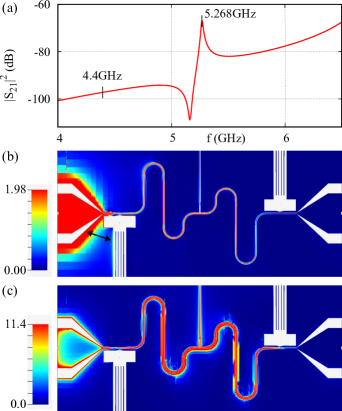
On the other hand, the coplanar waveguide resonator is strongly undercoupled. This leads to an asymmetry of signal level between input (drive) and output (detection) port, for both the resonant case and for the off-resonant case. Fig. 13 illustrates this with a numerical calculation of our bare resonator geometry (i.e., only the niobium layer and no further fabrication) using Sonnet Professional Sonnet Software, Inc. (2022); Rautio and Harrington (1987); Harrington (1993). Modeling the full chip is significantly more difficult because of the large differences in scale between meander filters and electrodes on one hand and the full coplanar waveguide resonator on the other hand Kellner et al. (2023). The signal transmission , plotted as function of frequency in Fig. 13(a), reaches in the calculation a maximum of at resonance .
The current distribution of the Sonnet calculation is plotted in Fig. 13(b) for , i.e., a strongly detuned red sideband drive as in our measurement. A closer look shows that in particular for such an off-resonant drive signal, direct crosstalk between the input port and the closeby nanotube contact electrodes (indicated by a black arrow) can cause additional ac signals on the nanotube. In the evaluation of Section III.3 this can lead to an overestimation of . Future device design will have to take this error mechanism into account.
An alternative estimate for the resonator photon number can be performed using the nominal attenuation and amplification values of the microwave setup. Following Sage et al. (2011) we calculate the photon number in the resonant case , , for a VNA output power of . With the attenuation in the input cable of excluding the cable loss, and a cable loss in both input and output each of , the resulting incoming power at the resonator input port is , see also the circut scheme of Fig. 2(a).
At resonance, we measure on the VNA a transmission attenuation of ; considering the amplification of low temperature and room temperature amplifiers and again the cable loss, we obtain as the power leaving the resonator.
This results in an insertion loss of
| (18) |
allowing us to calculate the circulating power
| (19) |
and finally the photon number in the resonator for the resonant driving case
| (20) |
To obtain the photon number for the case of red sideband drive we multiply with the ratio , resulting in , or at the drive power of the OMIT experiments , respectively.
The value of derived from the calibration in the main text is much larger. However, it is consistent with the broadening of the Coulomb oscillation in 9(a). Additionally, a much smaller photon number would result in an even much larger single photon coupling via the OMIT experiment than already found, at risk of an equally large overestimation of our already large Coulomb-blockade enhancement of the optomechanical coupling. While this naturally gives rise to optimism, it will have to be confirmed in future experiments.
Appendix B Cavity pull parameter
The frequency shift per displacement or cavity pull parameter is defined as
| (21) |
In a microwave optomechanical system with a deflection-dependent cavity (replacement) capacitance , using the relation it can be written as
| (22) |
Applying the same logic as in Blien et al. (2020), Supplement, Eqns. (26-29), we can translate a capacitance modulation into an effective gate volage modulation via and write out as
| (23) |
where is the geometric capacitance between resonator (gate) and nanotube (quantum dot).
References
- Aspelmeyer et al. (2014) M. Aspelmeyer, T. J. Kippenberg, and F. Marquardt, “Cavity optomechanics,” Rev. Mod. Phys. 86, 1391–1452 (2014).
- Chan et al. (2011) Jasper Chan, T. P. Mayer Alegre, Amir H. Safavi-Naeini, Jeff T. Hill, Alex Krause, Simon Groeblacher, Markus Aspelmeyer, and Oskar Painter, “Laser cooling of a nanomechanical oscillator into its quantum ground state,” Nature 478, 89–92 (2011).
- Teufel et al. (2011) J. D. Teufel, T. Donner, Dale Li, J. W. Harlow, M. S. Allman, K. Cicak, A. J. Sirois, J. D. Whittaker, K. W. Lehnert, and R. W. Simmonds, “Sideband cooling of micromechanical motion to the quantum ground state,” Nature 475, 359–363 (2011).
- Lecocq et al. (2015) F. Lecocq, J. B. Clark, R. W. Simmonds, J. Aumentado, and J. D. Teufel, “Quantum nondemolition measurement of a nonclassical state of a massive object,” Phys. Rev. X 5, 041037 (2015).
- Teufel et al. (2009) J. D. Teufel, T. Donner, M. A. Castellanos-Beltran, J. W. Harlow, and K. W. Lehnert, “Nanomechanical motion measured with an imprecision below that at the standard quantum limit,” Nature Nanotechnology 4, 820–823 (2009).
- Metcalfe (2014) Michael Metcalfe, “Applications of cavity optomechanics,” Applied Physics Reviews 1, 031105 (2014).
- Hüttel et al. (2009a) A. K. Hüttel, G. A. Steele, B. Witkamp, M. Poot, L. P. Kouwenhoven, and H. S. J. van der Zant, “Carbon nanotubes as ultrahigh quality factor mechanical resonators,” Nano Letters 9, 2547–2552 (2009a).
- Moser et al. (2014) J. Moser, A. Eichler, J. Güttinger, M. I. Dykman, and A. Bachtold, “Nanotube mechanical resonators with quality factors of up to 5 million,” Nature Nanotechnology 9, 1007–1011 (2014).
- Laird et al. (2015) E. A. Laird, F. Kuemmeth, G. A. Steele, K. Grove-Rasmussen, J. Nygård, K. Flensberg, and L. P. Kouwenhoven, “Quantum transport in carbon nanotubes,” Rev. Mod. Phys. 87, 703–764 (2015).
- Margańska et al. (2019) M. Margańska, D. R. Schmid, A. Dirnaichner, P. L. Stiller, Ch. Strunk, M. Grifoni, and A. K. Hüttel, “Shaping electron wave functions in a carbon nanotube with a parallel magnetic field,” Phys. Rev. Lett. 122, 086802 (2019).
- Schmid et al. (2020) Daniel R. Schmid, Peter L. Stiller, Alois Dirnaichner, and Andreas K. Hüttel, “From transparent conduction to Coulomb blockade at fixed hole number,” physica status solidi (b) 257, 2000253 (2020).
- Steele et al. (2009) G. A. Steele, A. K. Hüttel, B. Witkamp, M. Poot, H. B. Meerwaldt, L. P. Kouwenhoven, and H. S. J. van der Zant, “Strong coupling between single-electron tunneling and nanomechanical motion,” Science 325, 1103–1107 (2009).
- Lassagne et al. (2009) B. Lassagne, Y. Tarakanov, J. Kinaret, D. Garcia-Sanchez, and A. Bachtold, “Coupling mechanics to charge transport in carbon nanotube mechanical resonators,” Science 325, 1107–1110 (2009).
- Hüttel et al. (2010) A. K. Hüttel, H. B. Meerwaldt, G. A. Steele, M. Poot, B. Witkamp, L. P. Kouwenhoven, and H. S. J. van der Zant, “Single electron tunnelling through high-Q single-wall carbon nanotube NEMS resonators,” Phys. Stat. Sol. b 247, 2974 (2010).
- Häkkinen et al. (2015) P. Häkkinen, A. Isacsson, A. Savin, J. Sulkko, and P. Hakonen, “Charge sensitivity enhancement via mechanical oscillation in suspended carbon nanotube devices,” Nano Letters 15, 1667 (2015).
- Götz et al. (2018) K. J. G. Götz, D. R. Schmid, F. J. Schupp, P. L. Stiller, Ch. Strunk, and A. K. Hüttel, “Nanomechanical characterization of the Kondo charge dynamics in a carbon nanotube,” Phys. Rev. Lett. 120, 246802 (2018).
- Viennot et al. (2015) J. J. Viennot, M. C. Dartiailh, A. Cottet, and T. Kontos, “Coherent coupling of a single spin to microwave cavity photons,” Science 349, 408–411 (2015).
- Desjardins et al. (2017) M. M. Desjardins, J. J. Viennot, M. C. Dartiailh, L. E. Bruhat, M. R. Delbecq, M. Lee, M.-S. Choi, A. Cottet, and T. Kontos, “Observation of the frozen charge of a Kondo resonance,” Nature 545, 71 (2017).
- Stapfner et al. (2013) S. Stapfner, L. Ost, D. Hunger, J. Reichel, I. Favero, and E. M. Weig, “Cavity-enhanced optical detection of carbon nanotube Brownian motion,” Applied Physics Letters 102, 151910 (2013).
- Zhang et al. (2014) Mian Zhang, Arthur Barnard, Paul L. McEuen, and Michal Lipson, “Cavity Optomechanics with Suspended Carbon Nanotubes,” in CLEO: 2014 (2014), paper FTu2B.1 (Optica Publishing Group, 2014) p. FTu2B.1.
- Tavernarakis et al. (2018) A. Tavernarakis, A. Stavrinadis, A. Nowak, I. Tsioutsios, A. Bachtold, and P. Verlot, “Optomechanics with a hybrid carbon nanotube resonator,” Nature Communications 9, 662 (2018).
- Barnard et al. (2019) A. W. Barnard, M. Zhang, G. S. Wiederhecker, M. Lipson, and P. L. McEuen, “Real-time vibrations of a carbon nanotube,” Nature 566, 89–93 (2019).
- Regal et al. (2008) C. A. Regal, J. D. Teufel, and K. W. Lehnert, “Measuring nanomechanical motion with a microwave cavity interferometer,” Nature Physics 4, 555–560 (2008).
- Das et al. (2023) Soumya Ranjan Das, Sourav Majumder, Sudhir Kumar Sahu, Ujjawal Singhal, Tanmoy Bera, and Vibhor Singh, “Instabilities near ultrastrong coupling in a microwave optomechanical cavity,” Phys. Rev. Lett. 131, 067001 (2023).
- Blien et al. (2020) S. Blien, P. Steger, N. Hüttner, R. Graaf, and A. K. Hüttel, “Quantum capacitance mediated carbon nanotube optomechanics,” Nature Communications 11, 1363 (2020).
- Agarwal and Huang (2010) G. S. Agarwal and Sumei Huang, “Electromagnetically induced transparency in mechanical effects of light,” Physical Review A 81, 041803 (2010).
- Weis et al. (2010) S. Weis, R. Rivière, S. Deléglise, E. Gavartin, O. Arcizet, A. Schliesser, and T. J. Kippenberg, “Optomechanically induced transparency,” Science 330, 1520–1523 (2010).
- Kouwenhoven et al. (1997) L. P. Kouwenhoven, C. M. Marcus, P. L. McEuen, S. Tarucha, R. M. Westervelt, and N. S. Wingreen, “Electron transport in quantum dots,” in Mesoscopic Electron Transport, edited by L. L. Sohn, L. P. Kouwenhoven, and G. Schön (Kluwer, 1997).
- Pozar (2012) David M. Pozar, Microwave engineering, fourth edition ed. (Wiley, 2012).
- Simons (2001) R. N. Simons, Coplanar Waveguide Circuits, Components, and Systems (John Wiley & Sons, Inc., 2001).
- Gevorgian et al. (1995) S. Gevorgian, L. J. P. Linner, and E. L. Kollberg, “Cad models for shielded multilayered cpw,” IEEE Transactions on Microwave Theory and Techniques 43, 772–779 (1995).
- Petersson et al. (2012) K. D. Petersson, L. W. McFaul, M. D. Schroer, M. Jung, J. M. Taylor, A. A. Houck, and J. R. Petta, “Circuit quantum electrodynamics with a spin qubit,” Nature 490, 380–383 (2012).
- Göppl et al. (2008) M. Göppl, A. Fragner, M. Baur, R. Bianchetti, S. Filipp, J. M. Fink, P. J. Leek, G. Puebla, L. Steffen, and A. Wallraff, “Coplanar waveguide resonators for circuit quantum electrodynamics,” Journal of Applied Physics 104, 113904 (2008).
- Hornibrook et al. (2012) J. M. Hornibrook, E. E. Mitchell, and D. J. Reilly, “Superconducting resonators with parasitic electromagnetic environments,” (2012), arXiv:1203.4442 [cond-mat].
- Khalil et al. (2012) M. S. Khalil, M. J. A. Stoutimore, F. C. Wellstood, and K. D. Osborn, “An analysis method for asymmetric resonator transmission applied to superconducting devices,” Journal of Applied Physics 111, 054510 (2012).
- Petersan and Anlage (1998) P. J. Petersan and S. M. Anlage, “Measurement of resonant frequency and quality factor of microwave resonators: Comparison of methods,” Journal of Applied Physics 84, 3392–3402 (1998).
- Singh et al. (2014) V. Singh, S. J. Bosman, B. H. Schneider, Y. M. Blanter, A. Castellanos-Gomez, and G. A. Steele, “Optomechanical coupling between a multilayer graphene mechanical resonator and a superconducting microwave cavity,” Nature Nanotechnology 9, 820–824 (2014).
- Blien et al. (2016) S. Blien, K. J. G. Götz, P. L. Stiller, T. Mayer, T. Huber, O. Vavra, and A. K. Hüttel, “Towards carbon nanotube growth into superconducting microwave resonator geometries,” phys. stat. sol. (b) 253, 2385 (2016).
- Hao et al. (2014) Yu Hao, Francisco Rouxinol, and M. D. LaHaye, “Development of a broadband reflective T-filter for voltage biasing high-Q superconducting microwave cavities,” Applied Physics Letters 105, 222603 (2014).
- Wu et al. (2010) C. C. Wu, C. H. Liu, and Z. Zhong, “One-step direct transfer of pristine single-walled carbon nanotubes for functional nanoelectronics,” Nano Letters 10, 1032–1036 (2010).
- Blien et al. (2018) S. Blien, P. Steger, A. Albang, N. Paradiso, and A. K. Hüttel, “Quartz tuning-fork based carbon nanotube transfer into quantum device geometries,” Phys. Stat. Sol. B 255, 1800118 (2018).
- Tans et al. (1997) Sander J. Tans, Michel H. Devoret, Hongjie Dai, Andreas Thess, Richard E. Smalley, L. J. Geerligs, and Cees Dekker, “Individual single-wall carbon nanotubes as quantum wires,” Nature 386, 474 (1997).
- Braig and Flensberg (2003) S. Braig and K. Flensberg, “Vibrational sidebands and dissipative tunneling in molecular transistors,” Phys. Rev. B 68, 205324 (2003).
- Koch and von Oppen (2005) J. Koch and F. von Oppen, “Franck-Condon blockade and giant Fano factors in transport through single molecules,” Phys. Rev. Lett. 94, 206804 (2005).
- Sapmaz et al. (2006) S. Sapmaz, P. Jarillo-Herrero, Ya. M. Blanter, C. Dekker, and H. S. J. van der Zant, “Tunneling in suspended carbon nanotubes assisted by longitudinal phonons,” Phys. Rev. Lett. 96, 026801 (2006).
- Hüttel et al. (2009b) A. K. Hüttel, B. Witkamp, M. Leijnse, M. R. Wegewijs, and H. S. J. van der Zant, “Pumping of vibrational excitations in the Coulomb-blockade regime in a suspended carbon nanotube,” Phys. Rev. Lett. 102, 225501 (2009b).
- Stiller et al. (2020) P. L. Stiller, A. Dirnaichner, D. R. Schmid, and A. K. Hüttel, “Magnetic field control of the Franck-Condon coupling of few-electron quantum states,” Phys. Rev. B 102, 115408 (2020).
- Wunnicke (2006) O. Wunnicke, “Gate capacitance of back-gated nanowire field-effect transistors,” Applied Physics Letters 89, 083102 (2006).
- Schmid et al. (2012) D. R. Schmid, P. L. Stiller, C. Strunk, and A. K. Hüttel, “Magnetic damping of a carbon nanotube nano-electromechanical resonator,” New J. Phys. 14, 083024 (2012).
- Schmid et al. (2015) D. R. Schmid, P. L. Stiller, Ch. Strunk, and A. K. Hüttel, “Liquid-induced damping of mechanical feedback effects in single electron tunneling through a suspended carbon nanotube,” Appl. Phys. Lett. 107, 123110 (2015).
- Rechnitz et al. (2022) Sharon Rechnitz, Tal Tabachnik, Michael Shlafman, Shlomo Shlafman, and Yuval E. Yaish, “Mode coupling bi-stability and spectral broadening in buckled carbon nanotube mechanical resonators,” Nature Communications 13, 5900 (2022).
- Sazonova et al. (2004) V. Sazonova, Y. Yaish, H. Üstünel, D. Roundy, T. A. Arias, and P. L. McEuen, “A tunable carbon nanotube electromechanical oscillator,” Nature 431, 284–287 (2004).
- Witkamp et al. (2006) B. Witkamp, M. Poot, and H.S.J. van der Zant, Nano Lett. 6, 2904 (2006).
- Götz et al. (2019) Karl J. G. Götz, Felix J. Schupp, and Andreas K. Hüttel, “Carbon nanotube millikelvin transport and nanomechanics,” physica status solidi (b) 256, 1800517 (2019).
- Gouttenoire et al. (2010) Vincent Gouttenoire, Thomas Barois, Sorin Perisanu, Jean-Louis Leclercq, Stephen T. Purcell, Pascal Vincent, and Anthony Ayari, “Digital and FM demodulation of a doubly clamped single-walled carbon-nanotube oscillator: Towards a nanotube cell phone,” Small 6, 1060–1065 (2010).
- Kwon et al. (2004) Young-Kyun Kwon, Savas Berber, and David Tománek, “Thermal Contraction of Carbon Fullerenes and Nanotubes,” Physical Review Letters 92, 015901 (2004).
- Mounet and Marzari (2005) Nicolas Mounet and Nicola Marzari, “First-principles determination of the structural, vibrational and thermodynamic properties of diamond, graphite, and derivatives,” Physical Review B 71, 205214 (2005).
- Balandin (2011) Alexander A. Balandin, “Thermal properties of graphene and nanostructured carbon materials,” Nature Materials 10, 569–581 (2011).
- Chi et al. (2018) Xiannian Chi, Lei Wang, Jian Zhang, Jean Pierre Nshimiyimana, Xiao Hu, Pei Wu, Siyu Liu, Jia Liu, Weiguo Chu, Qian Liu, and Lianfeng Sun, “Experimental Evidence of Negative Thermal Expansion in a Composite Nanocable of Single-Walled Carbon Nanotubes and Amorphous Carbon along the Axial Direction,” The Journal of Physical Chemistry C 122, 26707–26712 (2018).
- Kozinsky et al. (2006) I. Kozinsky, H. W. Ch. Postma, I. Bargatin, and M. L. Roukes, “Tuning nonlinearity, dynamic range, and frequency of nanomechanical resonators,” Applied Physics Letters 88, 253101 (2006).
- Wu and Zhong (2011) C. C. Wu and Z. Zhong, “Capacitive spring softening in single-walled carbon nanotube nanoelectromechanical resonators,” Nano Letters 11, 1448–1451 (2011).
- Stiller et al. (2013) P. L. Stiller, S. Kugler, D. R. Schmid, C. Strunk, and A. K. Hüttel, “Negative frequency tuning of a carbon nanotube nano-electromechanical resonator under tension,” Phys. Stat. Sol. B 250, 2518–2522 (2013).
- Eichler et al. (2012) A. Eichler, M. del Álamo Ruiz, J. A. Plaza, and A. Bachtold, “Strong coupling between mechanical modes in a nanotube resonator,” Physical Review Letters 109, 025503 (2012).
- Eichler et al. (2011) A. Eichler, J Moser, J. Chaste, M. Zdrojek, I. Wilson-Rae, and Adrian Bachtold, “Nonlinear damping in mechanical resonators made from carbon nanotubes and graphene,” Nature Nanotechnology 6, 339 (2011).
- Solanki et al. (2010) Hari S. Solanki, Shamashis Sengupta, Sajal Dhara, Vibhor Singh, Sunil Patil, Rohan Dhall, Jeevak Parpia, Arnab Bhattacharya, and Mandar M. Deshmukh, “Tuning mechanical modes and influence of charge screening in nanowire resonators,” Physical Review B 81, 115459 (2010).
- Delbecq et al. (2011) M. R. Delbecq, V. Schmitt, F. D. Parmentier, N. Roch, J. J. Viennot, G. Fève, B. Huard, C. Mora, A. Cottet, and T. Kontos, “Coupling a quantum dot, fermionic leads, and a microwave cavity on a chip,” Phys. Rev. Lett. 107, 256804 (2011).
- Roschier et al. (2005) Leif Roschier, Mika Sillanpää, and Pertti Hakonen, “Quantum capacitive phase detector,” Phys. Rev. B 71, 024530 (2005).
- Meerwaldt et al. (2012) H. B. Meerwaldt, G. Labadze, B. H. Schneider, A. Taspinar, Ya. M. Blanter, H. S. J. van der Zant, and G. A. Steele, “Probing the charge of a quantum dot with a nanomechanical resonator,” Phys. Rev. B 86, 115454 (2012).
- Schleser et al. (2005) R. Schleser, E. Ruh, T. Ihn, K. Ensslin, D. C. Driscoll, and A. C. Gossard, “Finite-bias charge detection in a quantum dot,” Physical Review B 72, 035312 (2005).
- Beenakker (1991) C. W. J. Beenakker, “Theory of Coulomb-blockade oscillations in the conductance of a quantum dot,” Physical Review B 44, 1646–1656 (1991).
- Boller et al. (1991) K.-J. Boller, A. Imamoğlu, and S. E. Harris, “Observation of electromagnetically induced transparency,” Physical Review Letters 66, 2593–2596 (1991).
- Pirkkalainen et al. (2015) J.-M. Pirkkalainen, S. U. Cho, F. Massel, J. Tuorila, T. T. Heikkilä, P. J. Hakonen, and M. A. Sillanpää, “Cavity optomechanics mediated by a quantum two-level system,” Nature Communications 6, 6981 (2015).
- Pirkkalainen et al. (2013) J.-M. Pirkkalainen, S. U. Cho, Jian Li, G. S. Paraoanu, P. J. Hakonen, and M. A. Sillanpää, “Hybrid circuit cavity quantum electrodynamics with a micromechanical resonator,” Nature 494, 211–215 (2013).
- Pflanzer et al. (2013) Anika C. Pflanzer, Oriol Romero-Isart, and J. Ignacio Cirac, “Optomechanics assisted by a qubit: From dissipative state preparation to many-partite systems,” Physical Review A 88, 033804 (2013).
- Heikkilä et al. (2014) T. T. Heikkilä, F. Massel, J. Tuorila, R. Khan, and M. A. Sillanpää, “Enhancing optomechanical coupling via the Josephson effect,” Physical Review Letters 112, 203603 (2014).
- Rimberg et al. (2014) A. J. Rimberg, M. P. Blencowe, A. D. Armour, and P. D. Nation, “A cavity-Cooper pair transistor scheme for investigating quantum optomechanics in the ultra-strong coupling regime,” New Journal of Physics 16, 055008 (2014).
- Abdi et al. (2015) Mehdi Abdi, Matthias Pernpeintner, Rudolf Gross, Hans Huebl, and Michael J. Hartmann, “Quantum state engineering with circuit electromechanical three-body interactions,” Physical Review Letters 114, 173602 (2015).
- Gramich et al. (2013) Vera Gramich, Björn Kubala, Selina Rohrer, and Joachim Ankerhold, “From Coulomb-blockade to nonlinear quantum dynamics in a superconducting circuit with a resonator,” Physical Review Letters 111, 247002 (2013).
- Khan et al. (2015) Raphaël Khan, F. Massel, and T. T. Heikkilä, “Cross-Kerr nonlinearity in optomechanical systems,” Physical Review A 91, 043822 (2015).
- Schmidt et al. (2020) Philip Schmidt, Mohammad T. Amawi, Stefan Pogorzalek, Frank Deppe, Achim Marx, Rudolf Gross, and Hans Huebl, “Sideband-resolved resonator electromechanics based on a nonlinear Josephson inductance probed on the single-photon level,” Communications Physics 3, 1–7 (2020).
- Manninen et al. (2022) Juuso Manninen, Mohammad Tasnimul Haque, David Vitali, and Pertti Hakonen, “Enhancement of the optomechanical coupling and Kerr nonlinearity using the Josephson capacitance of a Cooper-pair box,” Physical Review B 105, 144508 (2022).
- Pistolesi et al. (2021) F. Pistolesi, A. N. Cleland, and A. Bachtold, “Proposal for a nanomechanical qubit,” Physical Review X 11, 031027 (2021).
- Kaikkonen et al. (2020) Jukka-Pekka Kaikkonen, Abhilash Thanniyil Sebastian, Patrik Laiho, Nan Wei, Marco Will, Yongping Liao, Esko I. Kauppinen, and Pertti J. Hakonen, “Suspended superconducting weak links from aerosol-synthesized single-walled carbon nanotubes,” Nano Research 13, 3433–3438 (2020).
- Elste et al. (2009a) Florian Elste, S. M. Girvin, and A. A. Clerk, “Quantum Noise Interference and Backaction Cooling in Cavity Nanomechanics,” Physical Review Letters 102, 207209 (2009a).
- Elste et al. (2009b) Florian Elste, A. A. Clerk, and S. M. Girvin, “Erratum: Quantum Noise Interference and Backaction Cooling in Cavity Nanomechanics [Phys. Rev. Lett. 102, 207209 (2009)],” Physical Review Letters 103, 149902 (2009b).
- Li et al. (2009) Mo Li, Wolfram H. P. Pernice, and Hong X. Tang, “Reactive Cavity Optical Force on Microdisk-Coupled Nanomechanical Beam Waveguides,” Physical Review Letters 103, 223901 (2009), publisher: American Physical Society.
- Weiss et al. (2013) Talitha Weiss, Christoph Bruder, and Andreas Nunnenkamp, “Strong-coupling effects in dissipatively coupled optomechanical systems,” New Journal of Physics 15, 045017 (2013).
- Kellner et al. (2023) N. Kellner, N. Hüttner, M. Will, P. Hakonen, and A. K. Hüttel, “Stepwise fabrication and optimization of coplanar waveguide resonator hybrid devices,” Phys. Stat. Sol. B , 2300187 (2023).
- Xiong et al. (2016) Wei Xiong, Da-Yu Jin, Yueyin Qiu, Chi-Hang Lam, and J. Q. You, “Cross-Kerr effect on an optomechanical system,” Physical Review A 93, 023844 (2016).
- Hu et al. (2015) Dan Hu, Shang-Yu Huang, Jie-Qiao Liao, Lin Tian, and Hsi-Sheng Goan, “Quantum coherence in ultrastrong optomechanics,” Physical Review A 91, 013812 (2015).
- Reinhardt et al. (2019) S. Reinhardt, C. Butschkow, S. Geissler, A. Dirnaichner, F. Olbrich, C. Lane, D. Schröer, and A. K. Hüttel, “Lab::Measurement — a portable and extensible framework for controlling lab equipment and conducting measurements,” Computer Physics Communications 234, 216–222 (2019).
- Sonnet Software, Inc. (2022) Sonnet Software, Inc., “Sonnet Professional 18.56,” (2022), a detailed list of references for the used algorithms can be found on the product website, https://www.sonnetsoftware.com/.
- Rautio and Harrington (1987) J.C. Rautio and R.F. Harrington, “An electromagnetic time-harmonic analysis of shielded microstrip circuits,” IEEE Transactions on Microwave Theory and Techniques 35, 726–730 (1987).
- Harrington (1993) Roger F. Harrington, Field computation by moment methods, IEEE Press series on electromagnetic waves (IEEE Press, Piscataway, NJ, 1993).
- Sage et al. (2011) Jeremy M. Sage, Vladimir Bolkhovsky, William D. Oliver, Benjamin Turek, and Paul B. Welander, “Study of loss in superconducting coplanar waveguide resonators,” Journal of Applied Physics 109, 063915 (2011).