High Q Hybrid Mie-Plasmonic Resonances in Van der Waals Nanoantennas on Gold Substrate
Abstract
Dielectric nanoresonators have been shown to circumvent the heavy optical losses associated with plasmonic devices, however they suffer from less confined resonances. By constructing a hybrid system of both dielectric and metallic materials, one can retain the low losses of dielectric resonances, whilst gaining additional control over the tuning of the modes with the metal, and achieving stronger mode confinement. In particular, multi-layered van der Waals materials are emerging as promising candidates for integration with metals owing to their weak attractive forces, which enable deposition onto such substrates without the requirement of lattice matching. Here we use layered, high refractive index WS2 exfoliated on gold, to fabricate and optically characterise a hybrid nanoantenna-on-gold system. We experimentally observe a hybridisation of Mie resonances, Fabry–Pérot modes, and surface plasmon-polaritons launched from the nanoantennas into the substrate. We achieve experimental quality factors of hybridised Mie-plasmonic modes to be 19 times that of Mie resonances in nanoantennas on silica, and observe signatures of a supercavity mode with a Q factor of 263 28, resulting from strong mode coupling between a higher-order anapole and Fabry–Pérot-plasmonic mode. We further simulate WS2 nanoantennas on gold with an hBN spacer, resulting in calculated electric field enhancements exceeding 2600, and a Purcell factor of 713. Our results demonstrate dramatic changes in the optical response of dielectric nanophotonic structures placed on gold, opening new possibilities for nanophotonics and sensing with simple-to-fabricate devices.
In the last decade, transition metal dichalcogenide (TMD) monolayers have attracted a large research effort owing to their direct band gap transition and useful opto-electronic properties [1], rendering the bulk material largely overlooked. More recently, nanoresonators utilising bulk TMDs to host Mie resonances [2] have gained interest, however these studies primarily focus on fabricating such structures on low refractive index dielectric substrates such as SiO2 [3, 4, 5, 6]. A hybrid TMD-nanoantenna-on-metal system has not been thoroughly explored, with previous work being dominated by numerical simulations. One of the first to be numerically characterised was a dielectric nanowire above a metallic substrate by Oulton et al. [7], which led to the prediction of hybrid dielectric-plasmonic modes. Since then, a variety of dielectric-metal nanodevices have been considered, from metallic nanoparticle-on-TMD monolayer systems [8, 9], to hybrid nanoantennas composed of silicon and gold coaxial layers [10, 11]. Furthermore, dielectric nanoantennas situated several nanometers above a silver substrate have been numerically analysed by Yang et al. [12]. Their work shows hybrid dielectric-plasmonic modes [12] with quality (Q) factors up to and Purcell enhancements of , along with strong electric field confinement in the nanoantenna-substrate gap. Shen et al. [13] built on this by simulating an hBN-WSe2 heterostructure placed within the gap and achieving strong light-matter coupling. Experimental work has so far been limited to silicon-based nanoresonators on metallic substrates. In 2018 Xu et al. fabricated silicon nanodisks on a gold substrate, realising an anapole mode [14]. The anapole was used to enhance third harmonic generation by two orders of magnitude compared to the same nanodisk on an insulating substrate. Maimaiti et al. fabricated a similar device composed of polycrystalline silicon nanodisks on a gold substrate, but with the introduction of an Al2O3 spacer layer between the nanodisk and substrate [15]. This led to an electric field enhancement in the spacer of over 40, and a Purcell factor of 300 for a vertically oriented dipole in simulation. In experiment, they demonstrated fluorescence enhancement, and surface-enhanced Raman spectroscopy of coupled molecules with a more stable signal than solely plasmonic nanodisks. Finally, and most applicable to this study, Dmitriev et al. fabricated silicon nanorings on gold with a layer of embedded quantum emitters between them [16]. They observed Mie resonances from the nanoring in dark field spectroscopy, along with strong directionality of the coupled emitters normal to the substrate.
TMDs present an attractive alternative to silicon-based nanophotonics for generating strong mode confinement owing to their higher refractive indices [17], whilst also having no absorption over large parts of the visible wavelength range [18]. Additionally, one can achieve high crystalline quality of thin films (from monolayer up to nm) required for fabrication of nanoantennas, through simple exfoliation from bulk TMDs [19]. Furthermore, they can be exfoliated onto a range of other materials owing to their inherent van der Waals attractive forces [1]. This avoids difficulties such as lattice matching requirements and growth in molecular beam epitaxy chambers, which are associated with fabricating nanoantennas from other conventional dielectrics such as GaAs and GaP. Use of TMDs thus opens new possibilities in the design and fabrication of hybrid dielectric-metallic structures of a variety of thicknesses, enabling advanced control of photonic and plasmonic resonances on the nanoscale.
In this study, we fabricate WS2 nanoantennas on a gold substrate and characterise their optical response with experimental dark field spectroscopy, which agrees well with finite-difference time-domain (FDTD) simulations. We carefully examine the Mie and anapole resonances within such devices, and observe dramatic changes in the mode structure compared to that of nanoantennas on silica, with improved Q factors. We use both simulation, and experimental scattering-type scanning near-field optical microscopy (s-SNOM) to confirm the presence of hybrid Mie-plasmonic modes [20], which can enhance surface plasmon-polaritons (SPPs) launched by illuminated nanoantennas. We observe a Fano lineshape for these modes, unlike the Lorentzian lineshape associated with Mie modes, therefore confirming the identification of hybrid resonances. We experimentally demonstrate that they can be easily tuned to different wavelengths by changing nanoantenna geometries. Such hybridised modes exhibit experimental Q factors up to 94, nearly a factor of 20 higher than Mie modes in nanoantennas on silica [21], highlighting potential applications in switching and sensing [22, 23, 24, 25].
We further explore strong mode coupling between a higher-order anapole mode (HOAM) and a Fabry–Pérot-plasmonic (FPP) mode within a WS2 nanoantenna on a gold substrate in both experiment and simulation. Such resonances can be tuned to realise an anti-crossing in the scattering spectra, with an experimental minimum energy splitting of 48 5 meV. At the point of anti-crossing, we observe signatures of a highly confined supercavity mode [26], with a Q factor of 263 28, resulting from the destructive interference of the HOAM and FPP mode outside of the hybrid nanoantenna structure. This offers one of the first practical solutions to realising a supercavity mode in finite-sized nanophotonic devices.
Finally, we model novel structures that include WS2 nanoantennas on top of 5 nm thick layers of hBN attached to a gold substrate. With this device, we numerically achieve strong electric field enhancement up to 2647 in the hBN spacer between the nanoantenna and gold. From this, we calculate Purcell enhancements up to 713 for a dipole polarised normal to the substrate within the hBN. This configuration offers the potential for enhancing the emission of coupled single photon emitters (SPEs), or interlayer and moiré excitons [27, 28] in TMD heterostructures placed within the gap.
Results
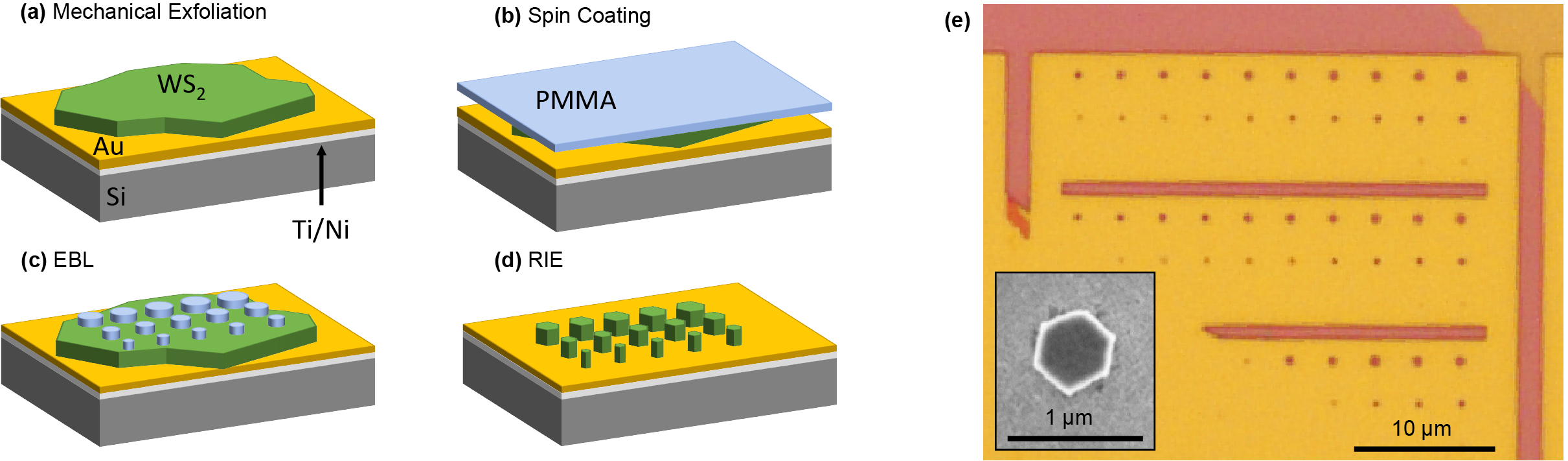
Sample Fabrication We realised WS2 nanoantennas on a gold substrate using well-established nanofabrication techniques (see Methods). We began by fabricating gold film substrates using two methods: electron-beam evaporation of gold onto a silicon substrate with either a titanium or nickel adhesion layer, and template-stripping [29]. We measured RMS roughness values down to 1.2 and 0.7 nm respectively, before mechanically exfoliating bulk WS2 [19] directly onto the gold. Flakes of varying thicknesses were found in each exfoliation run, measured using atomic force microscopy (AFM), before selecting those with thicknesses matching our simulations for nanoantenna fabrication. A positive resist was then spun onto our sample, before using electron beam lithography (EBL) to pattern arrays of circles of increasing radii from 100 to 400 nm. We then carried out reactive ion etching (RIE) to remove excess WS2 leaving behind nanoantennas. We used an isotropic etching recipe with SF6 gas (pressure and DC bias detailed in Methods) to achieve nanoantennas with hexagonal geometries. Fluorine radicals in the plasma etch the armchair axis of the WS2 crystal much faster than the zig-zag axis, leaving the adjacent etched nanostructure facets at 120° to each other [30, 6, 17]. The true radii of the nanoantennas, as measured by scanning electron microscopy (SEM), were smaller than those in the resist pattern due to the isotropic etching process, which slightly reduces their lateral size. The gold substrate is chemically inert to SF6. This means that it acts as a natural etch stop unlike SiO2, which would be etched along with the WS2, leaving the nanoantennas on a small pedestal of substrate material. Here, the use of gold eliminates this problem. Figures 1(a)-(d) illustrate the fabrication procedure, and Figure 1(e) shows both optical and SEM images of the finalised nanoantennas.
Dark Field Spectroscopy of WS2 Nanoantennas on Gold In order to optically characterise our fabricated samples, we carried out dark field spectroscopy on individual WS2 nanoantennas (monomers) on gold. We measured three different heights of nanoantennas (41, 78, 180 nm as measured by AFM) with a range of radii for each, and plot the normalised scattering intensity in Figures 2(a)-(c). Panels (d)-(f) show the simulated scattering cross sections for the same range of heights and radii using the FDTD method, exhibiting good agreement. Note that panels (c) and (f) correspond to double nanoantennas (dimers) with a gap between them on the order of 500 nm. We do not expect a significant change in the scattering intensity between monomers and dimers, especially for such large gap sizes [6].
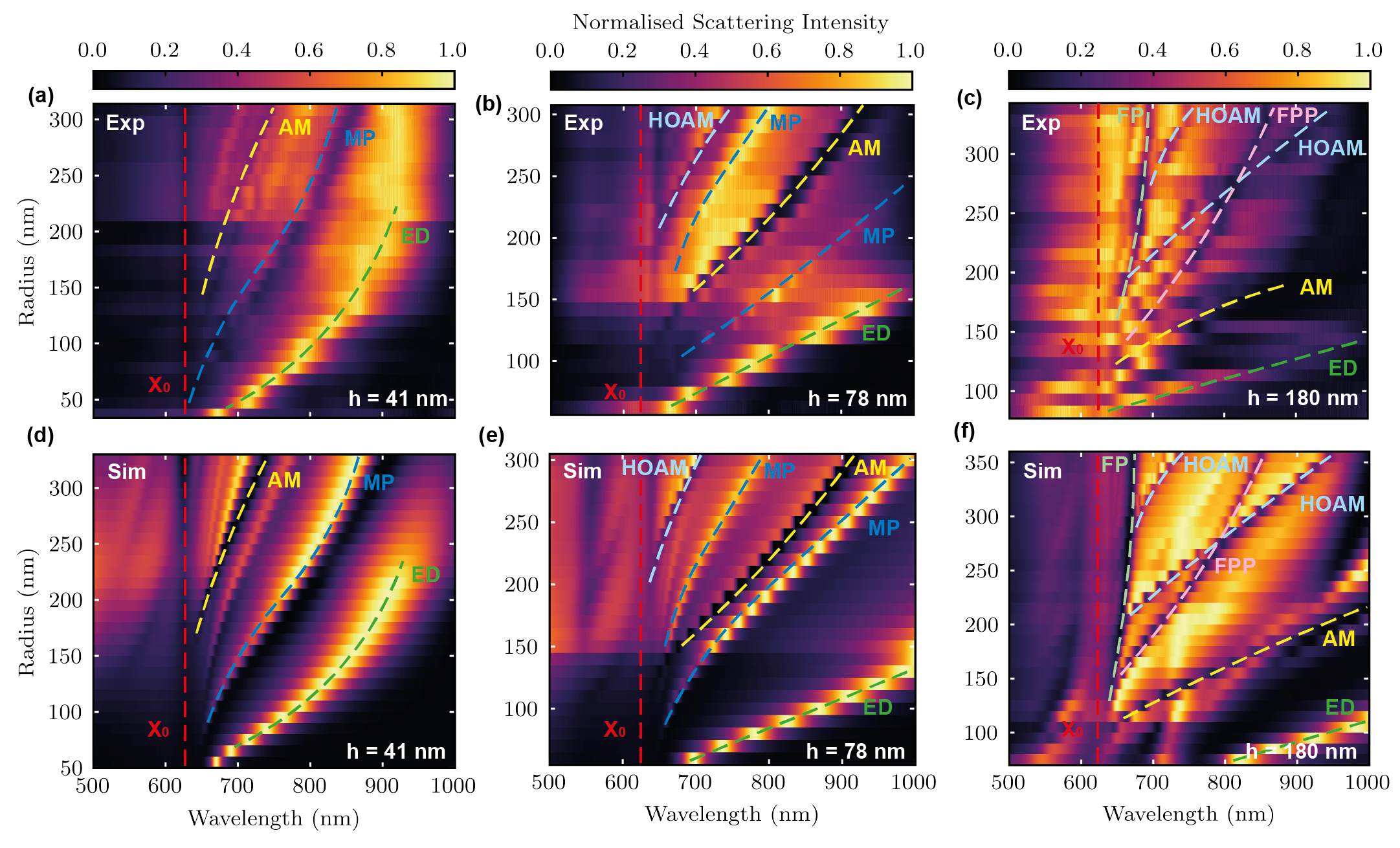
The mode structure becomes increasingly complex as we increase the nanoantenna height. In the simplest case of monomers with height 41 nm (Figures 2(a) and (d)), we observe a variety of maxima and minima in the scattering spectra that red-shift with increasing radius. These are known as Mie resonances [2], which are caused by bound charge oscillations within the WS2 crystal of the nanoantennas. An example is the electric dipole mode, which leads to increased scattering in the far-field as seen by the peaks labelled ED in Figure 2. The dark band can be identified as an anapole mode (AM), which is a destructive interference of the electric dipole mode and a magnetic toroidal mode [31], causing suppression of the scattering in the far-field [32]. The dip in scattering at a wavelength of 625 nm is due to WS2 excitonic absorption, where we observe avoided crossings with the Mie modes as previously reported [3]. We also label one of the modes MP, or Mie-plasmonic, which will be discussed in greater detail in the next section.
We extracted the quality factor of the ED and MP mode in experiment for WS2 nanoantennas on gold of height 41 nm throughout the range of radii in Figure 2(a). A Lorentzian function was fitted to the ED mode, and a Fano curve for the MP mode to calculate each respective Q factor. We extracted maximum Q factors of 24 0.6 for the ED mode of a nanoantenna with radius 48 nm, and 94 5 for the MP mode of a nanoantenna with radius 125 nm. Furthermore, we compared these Q factors to those previously measured in experiment for the ED mode in WS2 nanoantennas on a SiO2 substrate, which reach a maximum Q factor of 5 0.3 [21]. We observe a remarkable 19-fold increase in Q factor when comparing the MP mode in nanoantennas on a gold substrate, with the ED mode for nanoantennas on a SiO2 substrate.
This behaviour is further supported by simulation. We calculated maximum Q factors from Figure 2(d) of 61 0.6 for the ED mode of a nanoantenna of radius 40 nm on gold, and 137 1.6 for the MP mode of a nanoantenna of radius 100 nm on gold. By comparing these values to that of the ED mode in nanoantennas on a SiO2 substrate (Q = 4 0.1 [21]), we observe that the MP mode has a factor 34 higher Q factor than the ED mode for an all-dielectric system in simulation.
For h = 78 nm, we observe a narrowing of the electric dipole mode compared to h = 41 nm, along with a stronger red-shift with increasing radius. Additional modes such as the HOAM and two MP modes are visible in both simulation and experiment. When the height is increased to 180 nm, the mode structure becomes much more complex. Not only do we see anapole and higher-order anapole modes, but similar to previous simulations [33, 34, 35, 26, 36] and experiments [37, 38, 39, 40] of various dielectric nanostructures, we observe a Fabry–Pérot (FP) mode trapped between the TMD-gold interface at the bottom of the nanoantenna, and the TMD-air interface at the top. This mode shifts very little with changing radius, as would be expected from a vertically propagating FP mode. A more rigorous definition with comparison to FP mode theory is provided in Supplementary Note 1. We also observe an anti-crossing of a HOAM and FPP mode [40] in both the experimental and simulated scattering spectra of the dimer nanoantennas plotted in Figure 2(c) and (f). This occurs for nanoantennas with radii between 270 and 280 nm at a wavelength of around 800 nm, and is investigated in more detail later in this study.
Mie-Plasmonic Mode characterisation The mode structure of WS2 nanoantennas in vacuum and on low-index substrates is very different compared to the case with a gold substrate (see Supplementary Note 2 for a comparison of substrates). In order to gain further insight into the origin of the modes observed in WS2-on-gold nanoantennas, we simulated a monomer of a fixed geometry positioned at a varied distance above the gold substrate. We moved the nanoantenna towards the gold in 1 nm increments, starting at 20 nm, and calculated the scattering cross section as shown in Figures 3(a) and (b). This was done for monomer heights of 41 nm and 78 nm, and radii of 200 nm and 290 nm respectively, as studied in experiment and reported in Figure 2. In order to characterise the Mie resonances within the nanoantennas, we performed rigorous multipole expansions of the scattered light using the open source software MENP [41]. From this analysis, partial scattering cross sections attributed to the individual Mie modes can be extracted in order to assign them to their respective peaks and dips in the spectra. This was carried out for a monomer simulated in vacuum, as a homogeneous environment is necessary for the expansion.
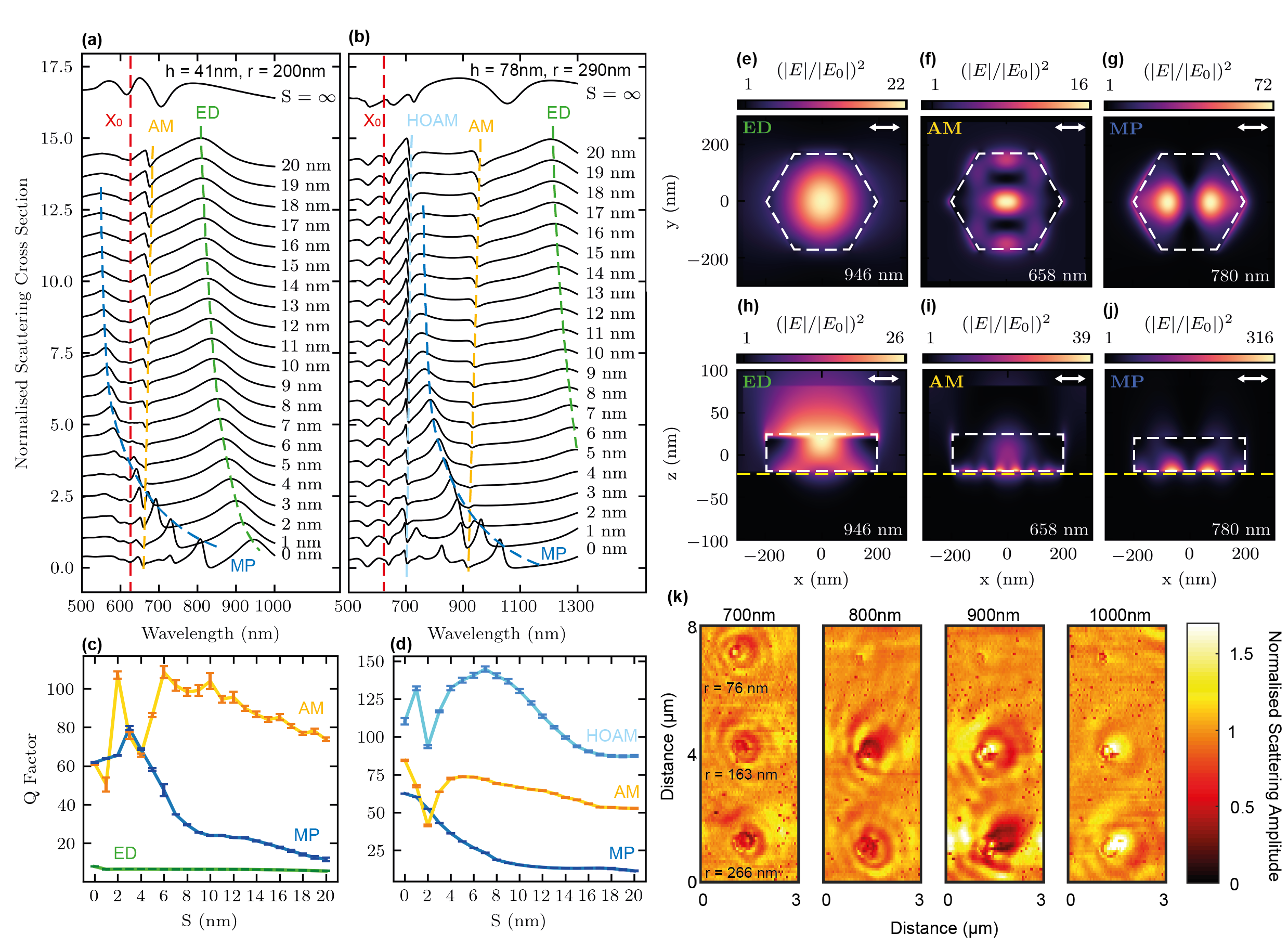
The green dashed line in Figures 3(a) and (b) follows the ED mode as S is decreased from 20 to 0 nm. The peak red-shifts by 140 nm and narrows for the nanoantennas in Figure 3(a) (h = 41 nm, r = 200 nm), therefore increasing the quality factor from 6 to 8 as shown in Figure 3(c). We observe the electric field distribution in the xz plane of the ED mode in Figure 3(h), where the central lobe protrudes upwards and out of the top of the nanoantenna with the introduction of the gold substrate, making the mode volume larger compared to in vacuum (see Supplementary Note 3). We therefore attribute the red-shift of the resonance to this increased mode volume. Conversely, the AM blue-shifts. Again, by considering the mode volume of the anapole resonance, as shown in Figure 3(i), we see a confinement of the mode owing to the gold substrate. The central field maxima extends slightly less outside of the nanoantenna and into the gold than compared to the case of a nanoantenna in vacuum (see Supplementary Note 3), hence we attribute the small blue-shift to this confinement. Furthermore, a resonance peak not seen in purely dielectric systems emerges in the spectra when S is reduced to the order of 10 nm, which we name Mie-plasmonic (MP) [42]. This peak is much sharper than that of the ED mode, and red-shifts more strongly by 159 nm from S = 4 nm to S = 0 nm for the h = 41 nm nanoantenna (Figure 3(a)). This behaviour is also seen for the MP mode of the h = 78 nm nanoantenna. An enlarged plot of the MP mode evolution is shown in Supplementary Note 4 for clarity, where an avoided crossing with the AM and exciton is also visible. The electric field distribution of this mode in the xz plane is very strongly localised to the gold-TMD boundary shown in Figure 3(j), which suggests that there is a contribution from plasmons, hence the naming Mie-plasmonic. This can also be observed for the ED and AM cases. However, the relative electric field enhancement at the boundary is much weaker. Interestingly, the MP mode takes a Fano lineshape in the spectra, which suggests an interference between a discrete state and a continuum of states [43, 24, 25]. Both the AM and HOAM also exhibit Fano lineshapes, whereas they can be described by a Lorentzian function for the case of nanoantennas on a dielectric substrate or surrounded by vacuum [44]. Supplementary Note 2 shows scattering cross sections for identical geometries of WS2 nanoantennas on gold, SiO2 and in vacuum for further confirmation of the different lineshapes with different substrates, suggesting that the gold substrate introduces an interference between a continuum (i.e. plasmons) and a discrete state (a Mie mode within the nanoantennas). Furthermore, the MP mode is not observed in the cases with nanoantennas on SiO2 or in vacuum, and neither does it appear in previous experimental or numerical dark field studies [3, 4, 6]. This evidence further supports that there is a hybridisation of both Mie and plasmonic modes present in our TMD nanoantenna-on-gold system.
In addition to the previously measured Q factors from Figure 2, we note that the AM and HOAM can reach even higher Q factors than the MP resonance when the distance between the nanoantenna and gold, S, is varied in simulation. This is shown in Figures 3(c) and (d). For a nanoantenna of height 78 nm and radius 290 nm, the MP mode reaches a maximum Q factor of 63 0.1 at S = 0 nm, whilst the AM has a maximum Q of 85 0.4 likely owing to the strong lateral confinement of this type of mode. The HOAM has an even larger maximum Q factor of 145 1.7 at S = 7 nm, suggesting an even stronger mode confinement. The dips in Q factor correspond to values of S where different modes cross each other in the scattering spectra, and so could be experiencing an interference effect. Whilst the Q factor of the ED mode in Figure 3(c) only increases very slightly with the introduction of a gold substrate, we see a localisation of the mode towards the substrate in the electric field distribution in Figure 3(h). This suggests that the ED mode also hybridises with plasmons in the gold along with the MP mode, but not as strongly.
To further characterise the nanoantennas and verify the mode hybridisation with plasmons, we performed s-SNOM imaging on arrays of WS2 nanoantennas of height 41 nm on gold, for a range of wavelengths from 700 - 1000 nm. s-SNOM involves probing the near-field response of a sample with an illuminated AFM tip, and using interferometric techniques to resolve both the amplitude and phase of the light scattered from the tip-sample interaction region. The tip can then be scanned across the sample, as in Figure 3(k), which shows the near-field scattering amplitude from the tip-sample interaction at each point, exhibiting the formation of ripples around the nanoantennas. Such ripples are the result of the tip illumination source interfering with SPPs on the gold, or with scattered light from features on the sample [45, 46, 47, 12, 48, 49, 50, 51, 52]. As the tip is moved across the sample, the contributions to the s-SNOM signal either interfere constructively or destructively. This produces a pattern of bright and dark fringes in the amplitude of the scattered light, which is observed as ripples. There are several methods by which this can happen, and each produce different interference patterns [52, 47, 45, 46]. However, there are two prominent methods in the case of nanoantennas on gold, the first being tip-launched SPPs. As the incident light reaches the tip, it becomes strongly localised at the tip’s apex. This strong near-field enhancement, and matching of the photon and plasmon wavevectors, causes tip-launched plasmons that emanate radially into the gold [53]. Such SPPs can then reflect from nearby structures and interfere with the incident light back at the tip. The second mechanism involves SPPs launched from the nanoantennas when illuminated [53], which travel to the tip and interfere with the incoming light. A combination of these two effects is observed in the ripple patterns in Figure 3(k).
As the incident wavelength is varied, the wavelength of the SPPs produced changes according to their dispersion relation, resulting in a change of the distance between the maxima of the ripple intensities. From Figure 3(k), we note that the distance between the ripple maxima increases with the wavelength of the excitation laser, but is constant across nanoantenna radius. This behaviour can also be seen in the s-SNOM images of the full array of nanoantennas in Supplementary Note 5. In contrast, the amplitude of the ripples corresponds strongly to the nanoantenna size and incident wavelength. By comparing the s-SNOM data in Figure 3(k) to the dark field spectra of the same nanoantennas in Figure 2(a) (see Supplementary Note 5 for direct comparison), we note a correlation between the amplitude of the SPP ripples and peaks in the corresponding dark field spectra. At shorter wavelengths, such as 700 nm, we observe the highest amplitude ripples from the smallest nanoantenna (r = 76 nm), followed by the r = 163 nm nanoantenna. This agrees with our experimental dark field data, where we see a strong resonant ED mode around 700 nm for the r = 76 nm nanoantenna, and the MP mode for the r = 163 nm nanoantenna (see Supplementary Note 5). As the incident wavelength is increased to 800 nm, the r = 76 nm nanoantenna begins to resonate less in the s-SNOM images, and the r = 163 nm nanoantenna shows a stronger SPP interference pattern, which we attribute to the excitation of the MP mode. At 900 nm illumination, both the r = 163 and 266 nm nanoantennas exhibit strong SPP ripples, following the red-shift of the ED mode in the dark field data (see Supplementary Note 5). Finally, at 1000 nm illumination wavelength, the amplitude of the SPP interference pattern around all of the nanoantennas is much lower, corresponding to the dip in overall scattering in the dark field spectra (Figure 2(a)). This observation demonstrates that van der Waals nanoantennas on gold can both scatter light to the far-field, and couple light to SPPs detectable in the near-field. Such SPPs can be further enhanced via the excitation of various Mie resonances, such as the ED and MP modes within the nanoantennas, hence providing further evidence for the coupling between Mie and plasmonic modes.
We do not observe SPP ripples on areas of gold far away from the nanoantennas (see Supplementary Note 6), as in this case, there are no features on the substrate to launch SPPs from. Only tip-launched SPPs are present, which travel away from the tip radially and have no edges to reflect back from. Therefore, no SPPs interfere with incident light at the tip, and so the s-SNOM image appears uniform. In Supplementary Note 6, we also show an area of the sample with pillars of resist between 25-35 nm in height on the gold, left over from the nanoantenna fabrication process. We observe negligible optical response from the resist pillars, which can be attributed to their low refractive index of 1.49 [54]. We therefore expect tip-launched plasmons to be mostly transmitted through such structures with little reflection back to the tip. In addition, light incident on the resist pillars is not expected to lead to well confined photonic resonances unlike the WS2 nanoantennas. This observation further supports our previous statement, suggesting that only the high refractive index WS2 nanoantennas can launch SPPs through strongly confined, hybrid Mie-plasmonic resonances.
Supercavity Mode in WS2 Nanoantennas on Gold In addition to the plasmon hybridisation discussed previously, we observe signatures of a highly-confined, non-radiating supercavity mode in both experiment and simulation by tuning the radii of WS2 nanoantennas on gold. This occurs as a result of the destructive interference of two different photonic modes outside of the nanoantenna, thus forming an extremely confined mode with a Q factor that, in theory, increases to infinity [26]. This is analogous to a Friedrich-Wintgen bound state in the continuum (BIC) [55], but for a finite-sized structure such as a nanoantenna. We observe signs of this in the form of an anti-crossing between the HOAM and FPP mode from Figure 2(c). In Figure 4(a), we investigate such behaviour in greater depth, by fitting the two modes to a coupled oscillator model.
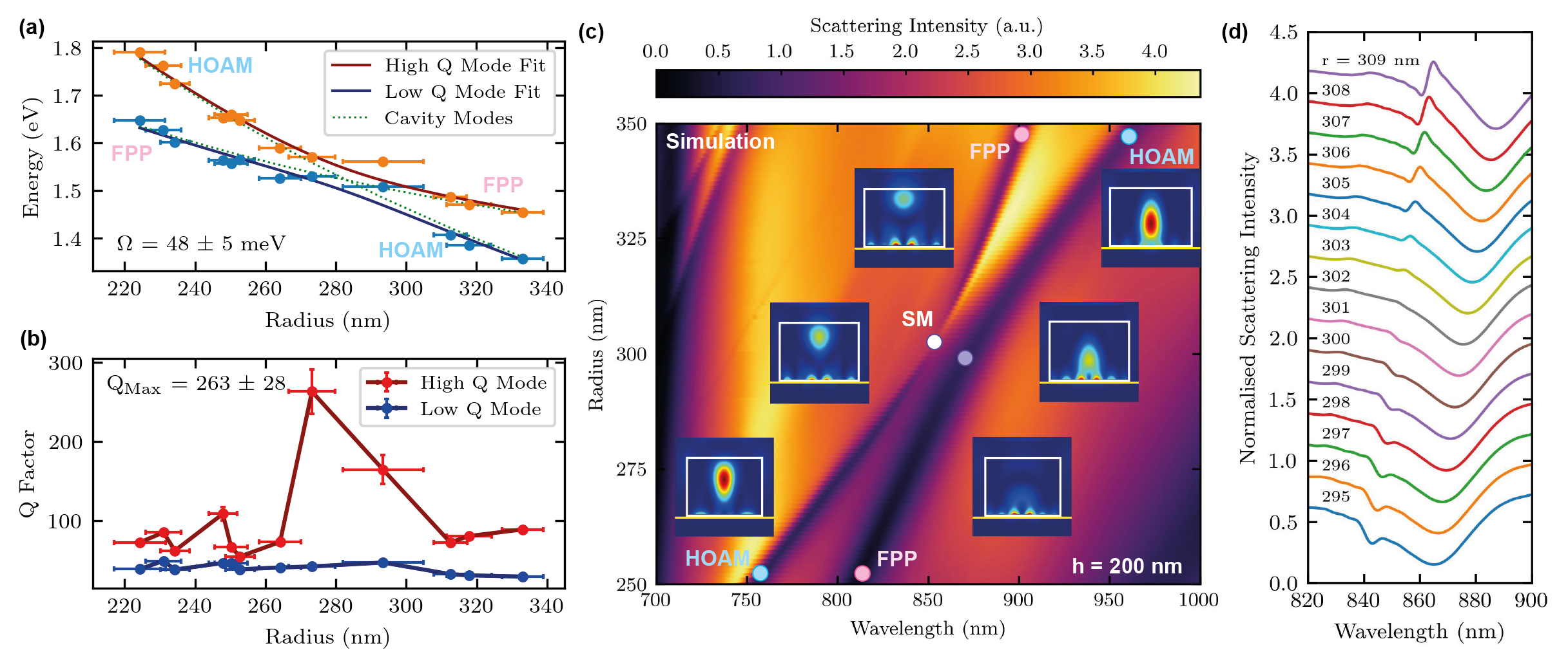
We first fitted the HOAM and FPP peaks with a double Fano formula to account for the hybridisation of the individual modes with plasmons, as detailed in Supplementary Note 7. We then extracted the peak center positions and plotted them in terms of energy against nanoantenna radius as shown in Figure 4(a). The error bars represent the uncertainty in the measured radii of each nanoantenna, with one data point at r = 293 nm showing a notably large error. We attribute this uncertainty to fabrication imperfections of this particular nanoantenna, which had a more irregular hexagonal cross-section than others when imaged with SEM, thus making the determination of its radius less reliable. The error in the fitted peak energy is negligible. The peak center positions were then fitted to a coupled oscillator model, yielding the upper and lower energy branches, shown as red and blue lines respectively. We refer to these as the high and low Q factor modes respectively. The green dotted lines represent the uncoupled HOAM and FPP mode for reference. From this fitting, we extract a minimum energy splitting of 48 5 meV. This is greater than the sum of the half linewidths of the uncoupled modes (34 1 meV), and hence we confirm strong mode coupling [36].
Furthermore, we calculate the Q factor of each peak and plot against nanoantenna radius in Figure 4(b). Whilst the low Q factor mode remains mostly constant, the high Q factor mode increases significantly at a radius of 273 nm. This radius corresponds to the closest point to the anti-crossing in Figure 4(a). We observe a maximum Q factor of 263 28; an order of magnitude larger than for the ED mode reported earlier in this study. This sharp increase in Q factor along with the observation of strong mode coupling are both signatures of a supercavity mode. We expect to observe much greater Q factors by fabricating more optimised structures with changes in radii down to 1 nm, in line with our simulations detailed in Supplementary Note 7.
In order to better understand the mode behaviour around the anti-crossing, we performed FDTD simulations of WS2 nanoantennas of height 200 nm on gold for a range of radii of 250 to 350 nm, with a much finer step in radius of 1 nm as shown in Figure 4(c). This greater height was chosen in order to red-shift the anti-crossing away from other modes in the scattering spectra to aid with fitting. The anti-crossing is clearly reproduced in the simulated spectra, and we extract an energy splitting of 37.5 0.3 meV (see Supplementary Note 7), agreeing with our experimental observations. We also simulate the electric field distribution within the nanoantennas at the points marked by the coloured circles in Figure 4(c). Away from the point of anti-crossing, the FPP mode displays clear maxima and minima in the xz plane as would be expected from a Fabry–Pérot mode confined vertically within the nanoantenna [36]. However, we also see evidence of hybridisation with plasmonic modes at the gold-WS2 boundary, similar to the MP modes described previously in this study. In addition, we do not observe this mode in WS2 nanoantennas on a SiO2 substrate in either simulation or experiment [21]. We therefore attribute this resonance to a hybrid Fabry–Pérot-plasmonic mode as a result of reflections from, and SPPs at, the WS2-gold interface. For smaller radii the FPP mode appears mostly plasmonic, with a field maxima near the bottom of the nanoantenna. In contrast, the HOAM field distribution is strongly localised at the center of the nanoantenna, exhibiting little hybridisation with plasmons. As the radius is increased, the electric field profile of the FPP mode hybridises with that of the HOAM to form a supercavity mode labelled SM. Upon increasing the nanoantenna radius further, the HOAM returns to a similar field distribution as before the anti-crossing, with the central field maxima localised closer to the gold interface. However, the FPP mode field maxima is pushed up towards the top of the nanoantenna, whilst retaining the characteristic plasmon field distribution at the bottom.
We further investigate the suppression of the high Q factor mode as the nanoantenna radius is tuned. Figure 4(d) shows individual simulated scattering spectra from Figure 4(c) for a range of radii close to the anti-crossing. Whilst the low Q factor mode at higher wavelength remains mostly the same, the high Q factor mode at lower wavelength becomes almost invisible for a radius of 302 nm. This suppression of scattering corresponds to the point where the HOAM and FPP mode destructively interfere near perfectly, forming a highly confined resonance within the nanoantenna. Our simulations thus provide additional evidence to support our observation of a supercavity mode in hybrid WS2-on-gold nanoantennas in experiment.
Electric Field Confinement Between WS2 Nanoantennas and Gold The strong localisation of the electric field at the TMD-metal boundary, depicted in Figure 3(j), prompted further study into Purcell enhancement of emitters at this position. We simulated the electric field distribution within an hBN layer of 5 nm thickness between a WS2 nanoantenna and the gold substrate as shown in Figure 5(a). hBN was chosen owing to its transparency throughout the visible wavelength range [56], low refractive index of 2.2 [57], and the presence of single photon-emitting defects, radiating at a variety of wavelengths from around 550 - 850 nm [58, 59, 60, 61]. The results are shown in Figures 5(b) and (c) for a nanoantenna of height 60 nm and radius 210 nm. The geometry was optimised for the maximum possible Purcell factor within the hBN layer over the wavelengths previously reported for hBN SPEs. We calculated a maximum electric field enhancement of 2647 within the hBN spacer at 773 nm wavelength (the MP mode); two orders of magnitude higher than the maximum field within the nanoantennas for the ED mode (Figure 3(h)), and one order of magnitude higher than that of the MP mode inside a nanoantenna directly on a gold substrate (Figure 3(j)). Based on these calculations, we spatially mapped the Purcell factor of a dipole emitter placed within the hBN (see Figure 5(a)), mimicking an SPE. This mapping is shown in Figures 5(e) and (f), where the dipole was oriented perpendicular (along z), and parallel (along x) to the substrate respectively.
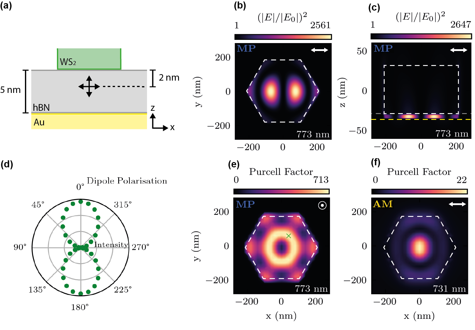
From Figure 5(e), we calculated a maximum Purcell factor of 713 for a dipole polarised perpendicular to the substrate at an emission wavelength of 773 nm (the MP mode), over two times greater than previously reported for silicon nanoantennas above gold for the same gap size [15]. Comparing to the dipole polarised parallel to the substrate in Figure 5(f), we observed a much lower maximum Purcell factor of 22 at 731 nm (the AM). We integrated the total emitted intensity of the dipole in all directions over a wavelength range of 550 - 850 nm for varying polarisations as shown in Figure 5(d). The dipole was located at the position of the Purcell factor maxima from Figure 5(e), marked by a green cross, with the polarisation being rotated in the xz plane. We observed a strong sensitivity to dipole orientation within the nanoantenna-substrate gap which suggests that particular enhancement is expected in structures where the dipole is oriented vertically. An example is hetero- and homobilayer TMDs, where interlayer excitons can be observed having the electron and hole in adjacent layers [62]. Therefore, we predict that by placing a TMD heterostructure within the nanoantenna-gold gap, one could achieve excitonic emission enhancement up to 32 times greater than for intralayer excitons in a similar structure, where the exciton lies in plane with the substrate.
Conclusion
In this study, we fabricated and characterised a hybrid dielectric-metallic nanophotonic system composed of WS2 nanoantennas on a gold substrate. Such TMD-based nanoantennas are easy to fabricate on metals using standard nanofabrication techniques owing to their van der Waals forces acting between the TMD thin film and the substrate, with the added benefit of gold providing a natural etch stop during RIE. We then investigated resonant Mie modes within the structures through simulation and observed excellent agreement in experimental dark field spectroscopy. We demonstrated that all the resonant modes identified can be tuned to different wavelengths simply by changing the nanoantenna radii, and that additional, higher-order modes can be introduced by increasing the nanoantenna height. Fano resonances were observed in WS2 nanoantennas on a gold substrate, not present in the same structures on SiO2, which we identify as a hybridisation of Mie modes and SPPs through both simulation and experiment. These modes couple to the far-field, as measured with dark field spectroscopy, and produce SPPs detectable in the near-field with s-SNOM imaging. The SPP intensities exhibited resonant behaviour, following the red-shift of the modes upon increasing nanoantenna radii, further supporting our claims of hybridised Mie-plasmonic modes. Such hybrid Fano resonances also have high Q factors, almost 20 times higher than Mie modes in nanoantennas placed on a low-index SiO2 substrate in experiment [21], hence enabling applications in switching and sensing [22, 23, 24, 25].
We further demonstrated strong mode coupling of Mie and Fabry–Pérot-plasmonic modes within WS2 nanoantennas on a gold substrate in experiment and simulation. We calculated a minimum energy splitting of 48 5 meV, and with careful tuning of the nanoantenna geometry we discovered signatures of a quasi-BIC supercavity mode at the point of anti-crossing, including a significantly increased experimental Q factor of over 260, and near complete suppression of scattering in simulation. To the best of our knowledge, the use of a gold substrate reveals one of the first realistic methods of achieving a supercavity mode in van der Waals nanoantennas in experiment.
Finally, we observed in simulations that very strong electric field enhancement of over 2600 occurs in a nanometer scale gap between the studied WS2 nanoantennas and gold substrate. For a gap filled with 5 nm of hBN, we calculated a Purcell factor of 713 for an emitter within the hBN polarised perpendicular to the substrate; 32 times higher than for parallel polarisation. This introduces opportunities for enhancing emitters placed in this nanoscale gap, such as SPEs in TMDs [63, 64, 65, 66, 67, 68, 69, 70, 71, 72, 73, 74] and hBN [58, 59, 60, 61], as well as interlayer excitons in TMD bilayers [62] and van der Waals heterostructures [75, 76, 77, 78, 79, 80].
We have shown experimentally that merits from both plasmonic and dielectric regimes can be achieved, and that hybrid Mie-plasmonic resonances can be tuned easily for any desired application by changing nanoantenna geometries, resulting in high Q factors not previously observed in solely dielectric nanoantennas. We believe that our hybrid nanoantenna system will open up additional pathways for future nanophotonic structures and resonators, with immediate applications for single photon emitters and photoluminescence enhancement in van der Waals heterostructures. Coupling of this system to other photonic devices such as waveguides, photonic crystals, and gratings, offers near limitless combinations for using TMDs and metals together to fabricate nano-optical circuits with strong field confinement and low losses.
Methods
FDTD Simulations In order to predict the behaviour of light within and around our nanoantennas, the software package Lumerical from Ansys was used to perform FDTD simulations.
Scattering Simulations The scattering cross-sections in Figure 2 were calculated by simulating WS2 nanoantennas of varying geometries on a semi-infinite gold substrate. To emulate dark field experiments as closely as possible, a total-field scattered-field (TFSF) plane wave source was used which subtracts the incident wave outside of its area of effect. This way, only the scattered light in the far-field was measured by a power monitor placed above the nanoantenna. The incident wave was set to propagate normal to the substrate and was polarised along the x axis. Anti-symmetric and symmetric boundary conditions were used along the x = 0 and y = 0 planes respectively, to reduce simulation time and memory requirements.
Field Distributions To visualise the electric and magnetic field distributions within and around the nanoantennas, frequency-domain field and power monitors which perform discrete Fourier transforms (DFTs) at chosen frequencies were used. The monitors were set as 2D surfaces through the middle of the nanoantennas used in the scattering simulations along various planes, and returned the electric and magnetic field intensities normalised to the incident, vacuum wave.
Purcell Factor Calculations We considered a dipole emitter placed in an hBN spacer between our WS2 nanoantennas and a gold substrate to emulate an SPE. The wavelength was set to a range of 550 - 850 nm and the orientation of the dipole rotated in the xz plane to consider different polarisations. The Purcell factor was then calculated as the total integrated power of the system divided by the total integrated power of the same dipole in vacuum.
Substrate Preparation The gold substrates were fabricated using either template stripping (used in the structures measured in Figure 2(a)) or electron beam evaporation of roughly 150 nm of 99.99% pure gold onto a silicon wafer with a 10 nm titanium (used in the structures measured in Figures 2(b)), or nickel layer (used in the structures measured in Figure 2(c)) to promote adhesion to the gold. These had rms roughness values down to 0.7 nm, 1.2 nm, and 2.5 nm respectively.
TMD Exfoliation WS2 bulk crystal from HQ-graphene was mechanically exfoliated onto the gold substrates by hand. A temperature of 105 °C was used to ensure good flake adhesion. Uniform thickness flakes of sizes 50 m and upwards were recorded for patterning.
Electron Beam Lithography A positive resist (ARP-9 AllResist GmbH) was first spin-coated onto the sample at 3500 rpm for 60s before heating for 2 minutes at 180°C. EBL was then performed using a Raith GmbH Voyager system at 50 kV accelerating voltage and 560 pA beam current. The pattern formed an array of circles of varying radii across the resist to cover several WS2 flakes.
Reactive Ion Etching A chemical etching recipe was used to achieve hexagonal nanoantenna geometries. Plasma etching was performed for 40 s with SF6 gas at 0.13 mbar pressure with a DC bias of 50V. The armchair crystal axis of the bulk WS2 was preferentially etched faster than the zigzag axis leading to 120° angles between them, forming hexagonal pillars [30]. The gold substrate was etched much slower than the WS2, and so acted as a natural etch stop, leaving nanoantennas on a flat gold surface, rather than on a pedestal of substrate material. The leftover resist was then removed using warm 1165 resist remover, before bathing in acetone, followed by IPA for 5 min respectively. A final UV-ozone treatment of 20 min removed any residual organic debris.
Dark Field Spectroscopy Spectroscopy involving illuminating a sample whilst rejecting the reflected light and collecting only the scattered light was achieved using a Nikon LV150N microscope with a fitted circular beam block between the illumination source (tungsten halogen lamp) and the dark field objective lens (50x with 0.8 NA). The beam block used was slightly smaller than the diameter of the beam, so that the central part was discarded and only the outer ring of light entered the objective via redirection from an annular mirror. The sample was illuminated at a high oblique angle causing light to be scattered from the sample. The vertically scattered light was then collected by the objective and passed back through the hole in the annular mirror towards a 50 m pinhole before a fiber coupler. The pinhole ensured that only light scattered at a low angle to the normal was allowed to propagate into the 100 m diameter core of the multi-mode fiber. Another fiber coupler then sent the beam into a free space path, where two achromatic lenses were used to minimise beam diversion along the path to the spectrometer. Finally, a single achromatic lens was used to focus the beam onto the slit of a Princeton Instruments spectrometer, where the wavelength components were separated and detected by a charge coupled device.
s-SNOM Probing of the near-field scattering from our samples at the nanoscale was done using a commercial neaspec modular s-SNOM system in conjunction with a Coherent Chameleon Compact OPO-Vis pulsed laser. This technique combined a sharp AFM tip with incident radiation to strongly confine near-fields at the tip-sample interface, and measure the phase and amplitude of the scattered light. The laser was aligned onto a Platinum-Iridium (PtIr) coated cantilever tip (NanoWorld Arrow NCPt), with radius of curvature less than 25 nm, using a parabolic mirror within the s-SNOM system. The beam made a 60° angle with the tip, and was polarised parallel to the plane of incidence (p-polarised), to maximise the component along the tip axis. A strongly-confined near-field was generated at the tip, which then interacted with the sample as it was scanned below. Background scattering signal owing to the large spot size (few microns) compared to the tip size, was suppressed using neaspec’s patented pseudo-heterodyne interferometry system. A reference beam with a phase modulation induced via an oscillating mirror was interfered with the scattered signal at the detector. This formed sidebands of frequency , where is the tapping frequency of the tip, and is the modulation frequency of the reference mirror. The detector then locked in at harmonics of the tapping and sideband frequencies in order to eliminate background signal. Through using pseudo-heterodyne detection, both the amplitude and phase of the scattered light were measured simultaneously.
The s-SNOM measurements in this report were demodulated at either the 3rd (Figure 3(k) and Supplementary Note 5) or 4th (Supplementary Note 6) harmonic of and the first sideband in order to reduce the background as much as possible, whilst still keeping a good signal to noise ratio.
Acknowledgements
S.A.R., P.G.Z., X.H., A.J.K., S.N., D.H. and A.I.T. acknowledge support from the European Graphene Flagship Project under grant agreement number 881603 and EPSRC grants EP/S030751/1, EP/V006975/1, EP/V006975/1 and EP/V026496/1. Yadong Wang and A.I.T. acknowledge support from UKRI fellowship TWIST-NANOSPEC EP/X02153X/1. Yue Wang acknowledges a Research Fellowship (TOAST) awarded by the Royal Academy of Engineering. S.A.R., P.G.Z., S.N. and D.H. acknowledge IT Services at The University of Sheffield for the provision of services for High Performance Computing.
Author Contributions
Yue Wang fabricated the gold film substrates. S.A.R. exfoliated bulk WS2 onto the gold substrates and conducted AFM to ascertain flake thicknesses. Yue Wang and X.H. patterned and etched the WS2 flakes into hexagonal nanoantennas using EBL and RIE. S.A.R. and Yadong Wang characterised nanoantenna radii through SEM. S.A.R. and P.G.Z. measured dark field spectra for all nanoantennas and analysed the results. S.A.R. and A.J.K. characterised the nanoantennas using s-SNOM imaging at different wavelengths. S.A.R., P.G.Z., S.N., and D.H. all contributed to FDTD simulations of the scattering spectra, electric field distributions, and Purcell factors. S.A.R., P.G.Z. and A.I.T. wrote the manuscript. A.I.T. managed the whole project.
References
- [1] Mak, K. F. & Shan, J. Photonics and optoelectronics of 2D semiconductor transition metal dichalcogenides. Nature Photonics 10, 216–226 (2016).
- [2] Mie, G. Beiträge zur Optik trüber Medien, speziell kolloidaler Metallösungen. Annalen der Physik 330, 377–445 (1908).
- [3] Verre, R. et al. Transition metal dichalcogenide nanodisks as high-index dielectric Mie nanoresonators. Nature Nanotechnology 14, 679–683 (2019).
- [4] Green, T. D. et al. Optical material anisotropy in high-index transition metal dichalcogenide Mie nanoresonators. Optica 7, 680–686 (2020).
- [5] Busschaert, S. et al. Transition metal dichalcogenide resonators for second harmonic signal enhancement. ACS Photonics 7, 2482–2488 (2020).
- [6] Zotev, P. G. et al. Transition metal dichalcogenide dimer nanoantennas for tailored light–matter interactions. ACS Nano 16, 6493–6505 (2022).
- [7] Oulton, R. F., Sorger, V. J., Genov, D., Pile, D. & Zhang, X. A hybrid plasmonic waveguide for subwavelength confinement and long-range propagation. Nature Photonics 2, 496–500 (2008).
- [8] Kleemann, M.-E. et al. Strong-coupling of WSe2 in ultra-compact plasmonic nanocavities at room temperature. Nature Communications 8, 1–7 (2017).
- [9] Liu, Y. et al. Strong coupling between two-dimensional transition metal dichalcogenides and plasmonic-optical hybrid resonators. Physical Review B 104, 205118 (2021).
- [10] Shibanuma, T., Grinblat, G., Albella, P. & Maier, S. A. Efficient third harmonic generation from metal–dielectric hybrid nanoantennas. Nano Letters 17, 2647–2651 (2017).
- [11] Sun, S. et al. Enhanced directional fluorescence emission of randomly oriented emitters via a metal–dielectric hybrid nanoantenna. The Journal of Physical Chemistry C 123, 21150–21160 (2019).
- [12] Yang, Y., Miller, O. D., Christensen, T., Joannopoulos, J. D. & Soljacic, M. Low-loss plasmonic dielectric nanoresonators. Nano Letters 17, 3238–3245 (2017).
- [13] Shen, S. et al. Tuning magnetic Mie-exciton interaction from the intermediate to strong coupling regime in a WSe2 monolayer coupled with dielectric-metal nanoresonators. Physical Review B 105, 155403 (2022).
- [14] Xu, L. et al. Boosting third-harmonic generation by a mirror-enhanced anapole resonator. Light: Science & Applications 7, 1–8 (2018).
- [15] Maimaiti, A., Patra, P. P., Jones, S., Antosiewicz, T. J. & Verre, R. Low-loss hybrid high-index dielectric particles on a mirror for extreme light confinement. Advanced Optical Materials 8, 1901820 (2020).
- [16] Dmitriev, P. A. et al. Hybrid dielectric-plasmonic nanoantenna with multiresonances for subwavelength photon sources. ACS Photonics 10, 582–594 (2023).
- [17] Munkhbat, B., Küçüköz, B., Baranov, D. G., Antosiewicz, T. J. & Shegai, T. O. Nanostructured transition metal dichalcogenide multilayers for advanced nanophotonics. Preprint at https://arxiv.org/abs/2202.04898 (2022).
- [18] Munkhbat, B., Wróbel, P., Antosiewicz, T. J. & Shegai, T. O. Optical constants of several multilayer transition metal dichalcogenides measured by spectroscopic ellipsometry in the 300–1700 nm range: High index, anisotropy, and hyperbolicity. ACS Photonics 9, 2398–2407 (2022).
- [19] Novoselov, K. S. et al. Two-dimensional atomic crystals. Proceedings of the National Academy of Sciences 102, 10451–10453 (2005).
- [20] Decker, M., Pertsch, T. & Staude, I. Strong coupling in hybrid metal-dielectric nanoresonators. Philosophical Transactions of the Royal Society A: Mathematical, Physical and Engineering Sciences 375, 20160312 (2017).
- [21] Zotev, P. G. et al. Van der Waals materials for applications in nanophotonics. Preprint at https://arxiv.org/abs/2208.06249 (2022).
- [22] Lee, E., Seo, I. C., Lim, S. C., Jeong, H. Y. & Jun, Y. C. Active switching and tuning of sharp Fano resonances in the mid-infrared spectral region. Optics Express 24, 25684–25696 (2016).
- [23] Chen, J., Gan, F., Wang, Y. & Li, G. Plasmonic sensing and modulation based on Fano resonances. Advanced Optical Materials 6, 1701152 (2018).
- [24] Miroshnichenko, A. E., Flach, S. & Kivshar, Y. S. Fano resonances in nanoscale structures. Reviews of Modern Physics 82, 2257 (2010).
- [25] Limonov, M. F., Rybin, M. V., Poddubny, A. N. & Kivshar, Y. S. Fano resonances in photonics. Nature Photonics 11, 543–554 (2017).
- [26] Rybin, M. V. et al. High-Q supercavity modes in subwavelength dielectric resonators. Physical Review Letters 119, 243901 (2017).
- [27] Tran, K. et al. Evidence for moiré excitons in van der Waals heterostructures. Nature 567, 71–75 (2019).
- [28] Huang, D., Choi, J., Shih, C.-K. & Li, X. Excitons in semiconductor moiré superlattices. Nature Nanotechnology 17, 227–238 (2022).
- [29] Ederth, T. Template-stripped gold surfaces with 0.4-nm rms roughness suitable for force measurements: Application to the Casimir force in the 20–100-nm range. Physical Review A 62, 062104 (2000).
- [30] Danielsen, D. R. et al. Super-resolution nanolithography of two-dimensional materials by anisotropic etching. ACS Applied Materials & Interfaces 13, 41886–41894 (2021).
- [31] Afanasiev, G. & Stepanovsky, Y. P. The electromagnetic field of elementary time-dependent toroidal sources. Journal of Physics A: Mathematical and General 28, 4565 (1995).
- [32] Miroshnichenko, A. E. et al. Nonradiating anapole modes in dielectric nanoparticles. Nature Communications 6, 1–8 (2015).
- [33] Bordo, V. Model of Fabry-Pérot-type electromagnetic modes of a cylindrical nanowire. Physical Review B 81, 035420 (2010).
- [34] Landreman, P. E., Chalabi, H., Park, J. & Brongersma, M. L. Fabry-Perot description for Mie resonances of rectangular dielectric nanowire optical resonators. Optics Express 24, 29760–29772 (2016).
- [35] Abujetas, D. R., Mandujano, M. A., Méndez, E. R. & Sánchez-Gil, J. A. High-contrast Fano resonances in single semiconductor nanorods. ACS Photonics 4, 1814–1821 (2017).
- [36] Bogdanov, A. A. et al. Bound states in the continuum and Fano resonances in the strong mode coupling regime. Advanced Photonics 1, 016001 (2019).
- [37] Friedler, I. et al. Solid-state single photon sources: The nanowire antenna. Optics Express 17, 2095–2110 (2009).
- [38] Sun, L., Ren, M.-L., Liu, W. & Agarwal, R. Resolving parity and order of Fabry–Pérot modes in semiconductor nanostructure waveguides and lasers: Young’s interference experiment revisited. Nano Letters 14, 6564–6571 (2014).
- [39] Frolov, A. Y. et al. Near-field mapping of optical Fabry–Perot modes in all-dielectric nanoantennas. Nano Letters 17, 7629–7637 (2017).
- [40] Gromyko, D. A. et al. Strong local field enhancement of Raman scattering observed in metal-dielectric gratings due to vertical Fabry-Perot modes of surface plasmon polaritons. Physical Review Applied 17, 024015 (2022).
- [41] Hinamoto, T. & Fujii, M. MENP: An open-source MATLAB implementation of multipole expansion for nanophotonics. OSA Continuum 4, 1640–1648 (2021).
- [42] Liu, T., Xu, R., Yu, P., Wang, Z. & Takahara, J. Multipole and multimode engineering in Mie resonance-based metastructures. Nanophotonics 9, 1115–1137 (2020).
- [43] Fano, U., Pupillo, G., Zannoni, A. & Clark, C. W. On the absorption spectrum of noble gases at the arc spectrum limit. Journal of Research of the National Institute of Standards and Technology 110, 583 (2005).
- [44] Svyakhovskiy, S. E., Ternovski, V. V. & Tribelsky, M. I. Anapole: Its birth, life, and death. Optics Express 27, 23894–23904 (2019).
- [45] Huber, A., Ocelic, N. & Hillenbrand, R. Local excitation and interference of surface phonon polaritons studied by near-field infrared microscopy. Journal of Microscopy 229, 389–395 (2008).
- [46] Bozhevolnyi, S. I. Near-field mapping of surface polariton fields. Journal of Microscopy 202, 313–319 (2001).
- [47] Kaltenecker, K. J. et al. Mono-crystalline gold platelets: A high-quality platform for surface plasmon polaritons. Nanophotonics 9, 509–522 (2020).
- [48] Yang, J., Hugonin, J.-P. & Lalanne, P. Near-to-far field transformations for radiative and guided waves. ACS Photonics 3, 395–402 (2016).
- [49] Luan, Y. et al. Imaging anisotropic waveguide exciton polaritons in tin sulfide. Nano Letters 22, 1497–1503 (2022).
- [50] Babicheva, V. E. et al. Near-field surface waves in few-layer MoS2. ACS Photonics 5, 2106–2112 (2018).
- [51] Zhang, C., Hugonin, J.-P., Greffet, J.-J. & Sauvan, C. Surface plasmon polaritons emission with nanopatch antennas: Enhancement by means of mode hybridization. ACS Photonics 6, 2788–2796 (2019).
- [52] Walla, F. et al. Anisotropic excitation of surface plasmon polaritons on a metal film by a scattering-type scanning near-field microscope with a non-rotationally-symmetric probe tip. Nanophotonics 7, 269–276 (2018).
- [53] Novotny, L. & Hecht, B. Principles of Nano-Optics (Cambridge University Press, Cambridge, 2012).
- [54] Zhang, X., Qiu, J., Li, X., Zhao, J. & Liu, L. Complex refractive indices measurements of polymers in visible and near-infrared bands. Applied Optics 59, 2337–2344 (2020).
- [55] Friedrich, H. & Wintgen, D. Interfering resonances and bound states in the continuum. Physical Review A 32, 3231 (1985).
- [56] Nguyen, D. C. et al. Visibility of hexagonal boron nitride on transparent substrates. Nanotechnology 31, 195701 (2020).
- [57] Gorbachev, R. V. et al. Hunting for monolayer boron nitride: Optical and Raman signatures. Small 7, 465–468 (2011).
- [58] Tran, T. T. et al. Robust multicolor single photon emission from point defects in hexagonal boron nitride. ACS Nano 10, 7331–7338 (2016).
- [59] Jungwirth, N. R. et al. Temperature dependence of wavelength selectable zero-phonon emission from single defects in hexagonal boron nitride. Nano Letters 16, 6052–6057 (2016).
- [60] Castelletto, S., Inam, F. A., Sato, S.-i. & Boretti, A. Hexagonal boron nitride: A review of the emerging material platform for single-photon sources and the spin–photon interface. Beilstein Journal of Nanotechnology 11, 740–769 (2020).
- [61] Sajid, A., Ford, M. J. & Reimers, J. R. Single-photon emitters in hexagonal boron nitride: A review of progress. Reports on Progress in Physics 83, 044501 (2020).
- [62] Louca, C. et al. Nonlinear interactions of dipolar excitons and polaritons in MoS2 bilayers. Preprint at https://arxiv.org/abs/2204.00485 (2022).
- [63] Sortino, L. et al. Bright single photon emitters with enhanced quantum efficiency in a two-dimensional semiconductor coupled with dielectric nano-antennas. Nature Communications 12, 1–9 (2021).
- [64] Kumar, S. et al. Resonant laser spectroscopy of localized excitons in monolayer WSe2. Optica 3, 882–886 (2016).
- [65] Srivastava, A. et al. Optically active quantum dots in monolayer WSe2. Nature Nanotechnology 10, 491–496 (2015).
- [66] Koperski, M. et al. Single photon emitters in exfoliated WSe2 structures. Nature Nanotechnology 10, 503–506 (2015).
- [67] Kumar, S., Kaczmarczyk, A. & Gerardot, B. D. Strain-induced spatial and spectral isolation of quantum emitters in mono-and bilayer WSe2. Nano Letters 15, 7567–7573 (2015).
- [68] Luo, Y. et al. Deterministic coupling of site-controlled quantum emitters in monolayer WSe2 to plasmonic nanocavities. Nature Nanotechnology 13, 1137–1142 (2018).
- [69] Blauth, M. et al. Coupling single photons from discrete quantum emitters in WSe2 to lithographically defined plasmonic slot waveguides. Nano Letters 18, 6812–6819 (2018).
- [70] Tripathi, L. N. et al. Spontaneous emission enhancement in strain-induced WSe2 monolayer-based quantum light sources on metallic surfaces. ACS Photonics 5, 1919–1926 (2018).
- [71] He, Y.-M. et al. Single quantum emitters in monolayer semiconductors. Nature Nanotechnology 10, 497–502 (2015).
- [72] Tonndorf, P. et al. Single-photon emission from localized excitons in an atomically thin semiconductor. Optica 2, 347–352 (2015).
- [73] Palacios-Berraquero, C. et al. Large-scale quantum-emitter arrays in atomically thin semiconductors. Nature Communications 8, 1–6 (2017).
- [74] Branny, A., Kumar, S., Proux, R. & Gerardot, B. D. Deterministic strain-induced arrays of quantum emitters in a two-dimensional semiconductor. Nature Communications 8, 1–7 (2017).
- [75] Hong, X. et al. Ultrafast charge transfer in atomically thin MoS2/WS2 heterostructures. Nature Nanotechnology 9, 682–686 (2014).
- [76] Chen, H. et al. Ultrafast formation of interlayer hot excitons in atomically thin MoS2/WS2 heterostructures. Nature Communications 7, 1–8 (2016).
- [77] Miller, B. et al. Long-lived direct and indirect interlayer excitons in van der Waals heterostructures. Nano Letters 17, 5229–5237 (2017).
- [78] Kunstmann, J. et al. Momentum-space indirect interlayer excitons in transition-metal dichalcogenide van der Waals heterostructures. Nature Physics 14, 801–805 (2018).
- [79] Merkl, P. et al. Ultrafast transition between exciton phases in van der Waals heterostructures. Nature Materials 18, 691–696 (2019).
- [80] Kamban, H. C. & Pedersen, T. G. Interlayer excitons in van der Waals heterostructures: Binding energy, Stark shift, and field-induced dissociation. Scientific Reports 10, 1–10 (2020).