Gate Tunable Josephson Diode in Proximitized InAs Supercurrent Interferometers
Abstract
The Josephson diode (JD) is a non-reciprocal circuit element that supports a larger critical current in one direction compared to the other. This effect has gained a growing interest because of promising applications in superconducting electronic circuits with low power consumption. Some implementations of a JD rely on breaking the inversion symmetry in the material used to realize Josephson junctions (JJs), but recent theoretical proposals have suggested that the effect can also be engineered by combining two JJs hosting highly transmitting Andreev bound states in a Superconducting Quantum Interference Device (SQUID) at a small, but finite flux bias. We have realized a SQUID with two JJs fabricated in a proximitized InAs two-dimensional electron gas (2DEG). We demonstrate gate control of the diode efficiency from zero up to around % at specific flux bias values which comes close to the maximum of % predicated in Ref. [R. S. Souto, M. Leijnse and C. Schrade, Phys. Rev. Lett. 129, 267702 (2022)]. The key ingredients to the JD effect in the SQUID arrangement is the presence of highly transmitting channels in the JJs, a flux bias and an asymmetry between the two SQUID arms.
I Introduction
A widely used device in semiconductor electronics is the junction, which is a nonreciprocal element with regards to current flow, able to conduct current primarily in one direction. The presently ongoing rapid scaling of quantum computers will require low-dissipative control electronics that operate close to the quantum chip at low temperatures. These requirements have renewed the question whether there exists a superconducting equivalent of the diode, namely a device that supports a larger supercurrent in one direction than in another: the Josephson Diode (JD) [1, 2].
In a conventional Josephson Junction (JJ) [3], the current-phase relation (CPR) is sinusoidal , with being the critical current of the junction and with the ground state corresponding to zero phase bias . For this conventional case, the positive critical current, is obviously equal to the negative one . Since the critical supercurrent is reciprocal, there is no superconducting diode-effect (SDE).
A general CPR can have a more complex dependence on the phase [4]. But in general, is a -periodic function and if either time-reversal symmetry or inversion symmetry is preserved, it is an odd function: [1]. It can therefore be written as a Fourier series composed of terms where is a positive integer and the terms for are higher harmonics. If higher harmonics are present, the CPR is called non-sinusoidal [5, 6]. Such a CPR still does not display a SDE.
A necessary but not sufficient condition for the SDE to occur is that time-reversal symmetry is broken. This can be achieved either by an external magnetic-field of or by means of ferromagnetic elements built into the device. S-F-S junctions, where F (S) denotes a ferromagnet (superconductor) were proposed [7, 8], and experimentally studied in various configurations [9, 10, 11]. These junctions typically display a shift in the CPR and are thus know as -junctions. The energy ground state moves from to . Despite the presence of a magnetic field and time-reversal symmetry thus being broken, these junctions do not display a SDE.
Both inversion symmetry and time-reversal symmetry are broken in so-called anomalous JJs, also known as junctions, where the ground state of the junction has an ‘anomalous’ shift to with [12]. This situation is achieved in multiband conductors with spin-orbit interaction [13, 14, 15, 16, 17, 18, 19]. Evidence for junctions has been found in experiments with nanowires with strong spin-orbit interaction [20] and in planar Josephson junction arrays [21]. An anomalous JJ is also a necessary condition, but on its own not sufficient. Indeed, a CPR of the form with is an anomalous JJ, but still with .
The SDE has been observed in materials that display magneto-chiral anisotropy. Here, the normal-state resistivity itself depends on the sign of the current density and the sign of the magnetic field [22, 23, 18]. While this is a small effect in normal metals, it can become large at the transition to a superconducting state [24, 25, 26]. Recently, a large SDE was also observed in a 2D NbSe2 superconductor with applied out-of-plane magnetic field [27] and even in field-free situations [28, 29, 1] including twisted graphene [30, 31, 32].
Further studies have also considered, among others, polarized supercurrents, magnetic domain walls, vortex pinning, combination of s-wave and p-wave pairing, as well as finite-momentum pairing as the origin of a SDE [33, 34, 35, 36]. A SDE was even reported in a scanning-probe microscopy study where a single magnetic impurity was addressed on the surface of a superconductor [37].
Lastly, topological materials with helical edge states can carry supercurrents with a strong SDE [38, 39, 40, 41]. This is evidenced in the highly asymmetric Fraunhofer pattern with the property that , where is the magnetic field. This arises because of lack of inversion symmetry between the supercurrent flowing along the two edges of the crystal [38]. This situation is very much alike an asymmetric SQUID.
Already in the 1970s, when superconducting interference devices were studied in great detail using tunnel junctions, point contact structures and Dayem bridges, it was recognized that the critical current of a SQUID can become non-reciprocal [42, 43, 44, 45]. The origin was understood to emerge from an asymmetry in the two SQUID arms, but the arms needed to have a non-negligible loop inductance, too. Although the CPR of each single junction was sinusoidal, the CPR became non-reciprocal for the SQUID device due to asymmetric loop inductances.
Today, tunable superconductor-semiconductor hybrid devices have become a flourishing research topic [46, 47, 48, 49, 50]. In particular, in JJ made of semiconducting weak links, the magnitude of the supercurrent is tunable by local gate electrodes and, in some devices, the shape of the CPR can be tuned from sinusoidal to highly non-sinusoidal. Consequently, these devices provide a platform for the engineering of the SDE with unprecedented tunability. This has recently been investigated theoretically in Ref. [51, 52]. It has been shown that one can achieve a large SDE by combining two non-sinusoidal JJs in a dc-SQUID at finite flux bias even with negligible loop inductances. In this case, the non-reciprocal transport originates from the interference between higher-order harmonics in CPR of the JJs.
In the current work, we use gate-controlled JJs fabricated in an InAs 2DEG proximitized by an Al layer [53, 54]. These rather wide junctions contain many channels with a distribution of transmission eigenvalues. The non-sinusoidal character is due to highly transmissive channels that are present in these devices [55, 56, 57, 58, 59, 60]. By tuning the asymmetry between the SQUID arms with the respective gate-voltages we show that we can achieve a SDE up to 30%. This comes close to the maximum theoretically predicted value [51].
In Sec. II we present the device geometry, the experimental set up and the basic characterization of the individual JJs. The non-reciprocal character of the dc-SQUID with JJs having a non-sinusoidal CPR is then shown in Sec. III. We also define an analytical framework with which we are able to distinguish possible origins of the JD effect. Finally, we discuss the measured gate tunability of the diode efficiency in Sec. IV and end with the conclusion in Sec. V.
II Device and Basic Properties
The circuit diagram of the device is shown in Fig. 1(a) and a coloured electron-microscopy picture is presented in Fig. 1(b).
The circuit consists of a dc SQUID formed by two planar JJs realized in a shallow InAs 2DEG proximitized by Al layer. The 2DEG is obtained from a quantum well grown on an InP substrate embedded in In0.75Ga0.25As layers of which the top layer is nm thick. The stack is terminated with an in-situ grown nm thin Al layer inducing superconductivity in the 2DEG. The SQUID loop and the leads are defined by etching the Al and, additionally, nm deep into the semiconductor stack. The top and bottom Josephson junctions (JJ1 and JJ2) in the two branches of the loop are formed by selectively removing the Al in the form of stripes with length nm and width m and m.
A set of gates, , and , are used to tune the critical current of the junctions by applying appropriate gate voltages , and . They are made of two Ti/Au layers, isolated from the Al and from each other by hafnium dioxide (HfO2) layers. extends over the whole width of JJ1, while is shaped to gradually deplete JJ2 laterally, creating a Superconducting Quantum Point Contact (SQPC). An additional gate, , can be use to fine tune the charge carrier density in the SQPC. However, throughout the experiment the QPC functionality is not used and is kept at V.

Our setup sources a current using a M resistor in series to a dc voltage superposed by a small ac component with frequency = 17.7 Hz, supplied by a lock-in amplifier. The ac component has an amplitude of nA.
The SQUID is additionally shunted at the source to ground with a resistor directly placed on the sample holder.
This shunt resistor has two purposes: a) it limits the maximum voltage that appears over the junction in the normal state, and thus, the heating; and (b) it adds damping to the device avoiding hysteretic switching when assessing the critical current in experiments.
We measure the differential resistance of the shunted device using a voltage amplifier and lock-in techniques. In all plots where a measured differential resistance is shown the shunt resistor was not subtracted. The measurements presented in the following were obtained with the SQUID device operating in a dilution refrigerator with a base temperature of mK.
In Fig. 1(c) we show the measured differential resistance of JJ1 (left) and JJ2 (right) as a function of gate voltage and bias current. In the following, we approximate the critical current of the ith-junction, , by the current bias value at which the maximum value in differential resistance is measured. Here, the bias current is swept from zero to A, looking at transitions from the superconducting to the normal state. From the measurements we extract . The critical current of both junctions can be tuned from a few nA close to pinch-off at negative gate-voltages V to approximately 1 A. The key features of these hybrid semiconducting-superconducting JJs are the gate tunable critical current and the non-sinusoidal CPR.
In the short-junction limit, i.e. for junctions with a length shorter than the superconducting coherence length in the normal metal, the zero temperature limit of the supercurrent is given by [5]:
| (1) |
Here, is the transmission probability per channel . In multichannel devices with disorder, a universal distribution function of transmission eigenvalues was obtained [61, 55, 62, 63]. The distribution is bimodal with many low transmissive channels that contribute little to the current, but also with some channels having a transmission probability close to 1. These high-transmissive channels lead to the overall non-sinusoidal character. This is approximated with an effective (but constant) transmission probability per channel and written as a single channel non-sinusoidal CPR given by:
| (2) |
For the later discussion of the measurements the critical current of the junction and a unit-less normalization parameter are introduced. The ratio is given by with the number of channels. Note, for the single junction we have and thus . It is also seen that for small values of the CPR approaches a sinusoidal dependence. From experimental curves, we deduce the critical current of each junction, and . Note, that only two parameters are independent.
As shown in Fig. 1(a) the total supercurrent across the SQUID is the sum of the currents flowing in both branches and through the two JJs:
| (3) |
The two junctions are described by and . The uniqueness of phase around the loop leads to the so-called fluxoid relation (modulo )
| (4) |
where denotes the externally induced flux, the superconducting flux quantum and the respective phase. In this form of the fluxoid relation the loop inductance has been neglected. For a finite loop inductance there is an additional flux contribution which depends on the currents and flowing in each arm. It has been shown that asymmetric loop inductances can also induce a superconducting SDE [45, 64, 65]. To estimate the role of loop inductances in our experiment we perform a full analysis with equations given in the appendix, specifically in App. E. Taking Eq. 3 and Eq. 4 together yields an effective superconducting junction with a CPR
| (5) |
For a simple sinusoidal CPR, the addition of the two terms yields a -junction without a SDE, even when the two JJ have different critical currents. In contrast, in the presence of higher order harmonics, which appear for a non-sinusoidal CPR, constructive and destructive interference effects, acting opposite for the two current bias directions, give rise to unequal critical currents , and thus to a SDE [51, 52].
III Josephson Diode Effect
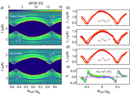
Figure 2(a) shows the differential resistance of the SQUID as a function of current bias and perpendicular magnetic field , the latter providing the flux through the SQUID loop. We have chosen a gate configuration with V for which the two critical currents are similar: A and A. A clear SDE is visible. For example, at the place of the orange arrow, we obtain A and A.
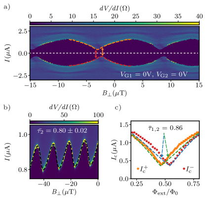
In this experiment, the current bias is swept from negative to positive values. This means that we measure the positive switching current , but on the negative side, we actually measure what is called the retrapping current where the device switches from the normal to the superconducting state. Due to dissipation, the junction can overheat in the normal state giving rise to a hysteresis between the switching and retrapping currents with the retrapping current being smaller in magnitude than the switching current. This would result in an artificial SDE. To exclude this, we have measured the same plot as in Fig. 2(a) but sweeping now from positive to negative bias currents. The comparison shows, see App. C, that the hysteresis between retrapping and switching currents is small and can be neglected. Physically, this is the case thanks to the low shunt resistant of which limits the voltage over the junction to V, and thus, limits the heating.
Another strong argument against an artificial effect is seen in Fig. 2(a) when one looks at the switching values at the place of the red arrow, where A and A. Here, the sign of the SDE is reversed, . This cannot be explained by a hysteresis between the switching and retrapping currents, since the retrapping current should always be smaller than the switching current.
As introduced before, a contribution from loop inductances may generate the SDE, too, if the loop inductances in the two arms are different. Applying finite element simulations, App. B, we obtain pH and pH. The relative phase shift between the two SQUID arms due to the loop inductances at a bias current is only , and gives a small contribution to the SDE. We properly simulate the effect of the loop inductances on the critical current of the SQUID in App. F and find that the loop inductances alone cannot explain the observed SDE in our experiment.
We also note that the measured CPR of the SQUID in Fig. 2(a) is periodic with a periodicity of T. Since this should correspond to an added flux quantum in the area of the inner SQUID hole, we obtain for . This is approximately a factor of bigger than the geometrical area defined by the etched square-shaped hole of size . This discrepancy can be attributed to the flux-focussing effect [66]. The magnetic field above the superconductor is screened by the Meissner effect leading to an enhanced magnetic field within the inner hole. The enhancement factor can be estimated by the ratio of the outer superconducting loop area of relative to , which yields a factor of in good agreement with the experiment.
In a sufficiently asymmetric SQUID configuration one can measure the CPR of the weak junction alone [6]. Figure 2(b) shows a measurement of the CPR of a single junction, obtained during the same cool-down. Here, V and V so that the current in JJ1 is large A and in JJ2 it is small A. In such a situation JJ1 acts as reference junction and the critical current of the weak junction JJ2 can be obtained from Eq. 5 as
| (6) | |||
| (7) |
where is the phase value for which JJ1 has its maximal value . Hence, we see that under the condition that the reference junction dominates, we obtain the phase dependence of the critical current of the weak junction from the flux dependence of the critical current of the SQUID. Applying Eq. 2 to fit the measured data yields for the effective transmission probability . This is a large value, showing that the CPR is strongly non-sinusoidal, something that is visibly seen in the graph of Fig. 2(b). If one makes use of the universal bimodal distribution function of transmission eigenvalues to determine [61, 55, 62, 63], one obtains . Including different devices nominally fabricated the same way, we always find a large effective transmission value of order in agreement with theoretical expectations for a multichannel disordered junction in the short junction limit.
In Fig. 2(c) we compare the oscillations of and as a function
with the simplified model of Eq. 5.
We take the measured critical currents of the two junctions as input parameters, i.e. A and A, and assume as a single fitting parameter. The best agreement is obtained for . We note, that a similar model calculation based only on loop inductances barely matches the measurement. It is shown as a comparison in App. F.
The fits for (green) and (blue) reproduce the relative shift along the flux axis very well. The shape of the curves is, however, not reproduced so well. In the region and respectively, the measured and curves are higher than what is obtained with the model. Deviations between the experimental and the modelled curves could be attributed to the choice of CPR used in the model. First, we considered an average transparency instead of a distribution of transparencies. Second, the expression of the current carried by the Andreev bound states could be different from Eq. 2, since our junctions could be in a regime intermediate to the short and long junction limit. And, in the third place, spin-orbit effects may affect the CPR, too. For junctions of similar length in the same material system, it has been shown that spin-orbit interaction splits the ABS into spinful states with different dispersion relations [67]. Noticeably, the experiment indicates that these deviations result in an increase of the SDE compared to what is predicted by the simple model.
Having established that a SDE appears in a SQUID with junctions having a non-sinusoidal CPR with asymmetry, we summarize in Table 1 the necessary conditions for the SDE (DE). To describe the asymmetry we introduce two asymmetry parameters and for the critical currents and the effective transmission probabilities, respectively:
| (8) |
| SDE | |||
|---|---|---|---|
| n.a. | no | ||
| n.a. | no | ||
| no | |||
| yes | |||
| yes | |||
| yes |
An extended table, which also considers the effect of loop inductances, is presented in App. G. It shows that the diode effect appears when the SQUID arms are asymmetric. The only exception is for sinusoidal JJs, where an asymmetry in the critical currents in not enough to produce a diode effect.
IV Gate Tunable Diode Efficiency
The SDE can be quantified via the diode efficiency, defined as
| (9) |
In Fig. 3, we show the magnitude of the diode efficiency as a function of external flux for different gate configurations as obtained from the experiment (left) and as calculated from the model (right). In the model, we make use of the relation between critical current and gate voltage of the individual junctions and use these values as input parameters in the first approximation. We also use the simulated loop inductance values from which we obtain the phase response due to screening , the loop inductance asymmetry with , , and and the respective mean values. We assume that the effect of the gate voltage is mainly to change the critical current value through the number of channels , while roughly stays constant. We fix , but we note that the calculated plot is insensitive if one varies between and .
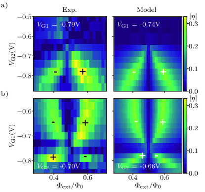
In Fig. 3(a), we plot for different values of at fixed . Both in the experiment and in the model, drops for V. As seen in Fig. 1(c), this corresponds to a gate configuration with , so that . As expected, the absence of critical current asymmetry decreases the diode efficiency. To obtain in the model the same diode efficiencies as measured, we had to increase the critical current of JJ1. In the experiment, we had fixed at V, which would correspond to nA. However, in order to match the model with the data, we had to use nA, corresponding to V, as indicated in the top left corner of the figure. Without this correction, the measured values would have been larger than what the model predicts. We attribute this difference in gate voltage to gate-jumps that occur from time-to-time. We note, that there are days between the measurements in Fig. 1(c) and in Fig. 2(a)
In Fig. 3(b) we show the dependence of as a function of at fixed . As before, to match the model to the experiment, we had to increase from the initially measured value of nA at to nA, which correspond to measured at V.
Both in the experiment and in the model one can observe the typical butterfly pattern of as predicted in Ref. [51]. The two arms of maximum meet at the point of minimum asymmetry at for V and V for (a) and (b) respectively, where drops to .
The model qualitatively reproduce the gate dependence of the diode efficiency very well. We obtain a maximum of from the experiment. This efficiency is much larger than what has previously been obtained in a SQUID with asymmetric loop inductance [68]. Taking a SQUID model with a single channel JJ junction, we numerically find for the maximum efficiency . This is obtained for and or the reversed. This could be achieved by combining a single channel ballistic Josephson junction realized in atomic contacts [6] with a semiconductor-superconductor hybrid device as we have discussed here.
V Conclusion
In conclusion, we have investigated the origin of the Superconducting Diode Effect (SDE) in a supercurrent interferometer realized in a proximitized InAs quantum well stack. We show that in such a system the SDE can originate from the non-sinusoidal character of the JJs, and hence, reflecting a subtle interference between higher-order harmonics of the CPRs of the individual JJs. In addition to higher harmonics, an asymmetry either in the composition of the Fourier components in the CPR or in the critical current of the two JJ, and a finite flux bias is required to obtain a SDE. These later conditions ensure that time-reversal symmetry and inversion symmetry are both broken. A similar conclusion was drawn by a recent experimental study in three terminal devices, where a SDE was realized [69]. Further, during the reviewing process we got aware of a similar study in a dc SQUID realized in a Ge quantum well structure [70]. Future directions include the possibility to concatenate more SQUIDs in parallel in order to further increase the diode efficiency as was proposed in Ref. [51].
Acknowledgements.
We thank C. M. Marcus for his support in initiating this work and collaboration. This research was supported by the Swiss National Science Foundation through grants No 172638 and 192027, and the QuantEra project SuperTop. We further acknowledge funding from the European Union’s Horizon 2020 research and innovation programme, specifically a) from the European Research Council (ERC) grant agreement No 787414, ERC-Adv TopSupra, (b) grant agreement No 828948, FET-open project AndQC, c) grant agreement 847471, project COFUND-QUSTEC, and d) grant agreement 862046, project TOPSQUAD. Constantin Schrade acknowledges support from the Microsoft Corporation and Christian Schönenberger from the Swiss Nanoscience Institute (SNI). All data in this publication is available in numerical form at: https://doi.org/10.5281/zenodo.7733057.Appendix A Fabrication & Measurement Set-up
The wafer used in this experiment was grown by molecular beam epitaxy (MBE). The stack consists from bottom to top of an InP substrate, a 1-m-thick buffer realized with In1-xAlxAs alloys, a 4 nm In0.75Ga0.25As bottom barrier, a 7 nm InAs layer, a 10 nm In0.75Ga0.25As top barrier, two monolayers of GaAs acting as stop etch layer, and 10 nm of Al deposited without breaking the MBE vacuum. The two-dimensional electron gas is characterized from a Hall bar devices and shows a peak electron mobility of for an electron density of , corresponding to an electron mean free path of nm.
The device is fabricated using standard electron beam lithography techniques. The MESA is electrically isolated by first removing the top Al film with Al etchant Transene D, followed by a deep III–V chemical wet etch with H2O:C6H8O7:H3PO4:H2O2 (220:55:3:3). Next, the Al film on the mesa is selectively etched with Al etchant Transene D to define the planar JJ. Electrostatic gates are made of two Ti/Au layers, isolated from the Al and from each other by hafnium oxide (HfO2) layers grown by atomic layer deposition (ALD) at a temperature of °C over the entire sample. The first layer of gates is made of electron-beam evaporated Ti/Au ( nm/ nm) on top of nm HfO2. Connections to the external circuit are obtained by evaporating Ti/Au ( nm) leads at 17° to overcome the MESA step. A second layer of gates, made of angle-evaporated Ti/Au ( nm), is patterned on top of nm of HfO2.
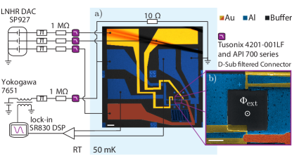
Measurements are carried out in a Triton 200 cryogen-free dilution refrigerator with a base temperature of mK. An overview of the measurement set-up is shown in Fig. 4. The setup sources a current using a M resistor in series to a dc voltage source on which a small ac component with frequency = 17.7 Hz, supplied by a lock-in amplifier, is superposed. This current is applied to the source contact of the SQUID on the left with the drain contact on the right side galvanically connected to ground. The SQUID is shunted at the source to ground with a resistor . This shunt resistor is directly placed on the sample holder. In addition, a finger capacitance of pF is patterned in parallel to the SQUID (lower right of the optical image). The original purpose of the capacitance was to increase the quality factor of the Josephson junctions. However, its effect is negligible, since the capacitance provided by the leads is larger. We measure the differential resistance of the shunted device using a voltage amplifier and lock-in techniques. The flux through the SQUID is generated by a vector magnet.
Appendix B Estimation of Loop Inductances
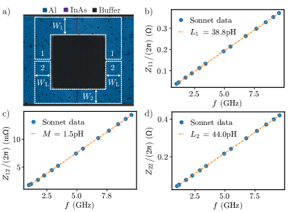
In the following we will detail the evaluation of the inductance of the loop branches. The loop geometry is defined as indicated by the white dashed lines in Fig. 5(a). The width of the two branches corresponds to the junctions width in the upper and lower path, = m, = m, and the width on the left and right sides it is set equal to = m. In reality there is no lateral confinement in the superconductor. Hence, the artificial confinement increases the inductance values so that the simulated inductances for this geometry yield upper bounds to the inductances of the device. With finite-element simulations performed in Sonnet, we compute the two-port impedances with for different frequencies. The impedance is evaluated between two sets of floating co-calibrated ports, positioned on the left and right side of the loop. In the simulation we use InP as a substrate, with a relative dielectric constant . The kinetic inductance of the Al film is evaluated by measuring the temperature dependence of the resistance of an Al bar realized on a different chip from the same wafer. We measure a critical temperature of K and a normal state resistance of . The kinetic sheet inductance is then obtained through the low frequency limit of the Mattis-Bardeen screening theory [71, 72, 73]:
| (10) |
Here, is the normal state sheet resistance, the zero-temperature BCS gap and the absolut etemperature. Using Eq. 10 we extract nH.
Appendix C Retrapping versus Switching Current
In Fig. 6 we compare the switching current with the retrapping current values. We show that the two values coincide in this experiment to a good accuracy. We think that this is due to the low parallel resistor which keeps the voltage over the junction small in the normal state, hence, reducing overheating effects. Additionally, the shunt resistor adds damping at the plasma frequency of the junctions, which reduces the quality factor.
The two measurements in Fig. 6(a) were obtained for exact the same parameter settings, except for the direction of current-bias sweep. In the upper (lower) measurement the current was decreased (increased) starting with positive (negative) values at A ( A) and sweeping down (up) to A ( A). (b) shows the critical and retrapping current, and , extracted from the downsweep data at positions where the differential resistance shows a peak. (c) shows the same, but extracted from the upsweep data. On sweeping downwards, we denote the negative critical current as and the positive retrapping current as . In analogy, on sweeping upwards, the positive critical current is denoted by and the negative retrapping current by . In (d) we compare the positive and negative critical currents, both obtained in a proper way using oppositive sweep directions.
Now we can compare the extracted diode efficiency for three cases: i) for the case when we extract the critical currents from sweeping the current bias into negative direction only, , ii) into positive direction only, , and iii), when we deduce the critical current properly, . The three curves are directly obtained from the graphs (b)-(d). All three methods yield qualitatively the same efficiencies with no significant differences. Importantly, one clearly cannot say that would yield in general lower efficiencies.
Appendix D SQUID Oscillations at Different Gate Voltages
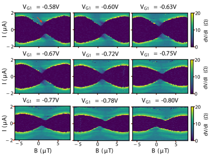
In this appendix we show how the SQUID pattern develops when the critical current of one junction is tuned from being larger, equal and finally smaller than the critical current of the other junction. Fig. 7 shows the differential resistance of the SQUID as a function of current bias and perpendicular magnetic field. is fixed at V, while is swept from V to V. As extracted from Fig. 1(c), nA, while A and nA (gate voltages are given in units of V).
The sign of the diode efficiency is mirrored with respect the magnetic field value corresponding to half flux quantum when the critical current asymmetry between the two junctions changes sign. We also notice a dip in differential resistance developing around half flux quantum that evolves with (see arrow in Fig. 7).
Appendix E Model Including Loop Inductances
As introduced in the main text, we model the current-phase relation of a single junction with
| (11) |
where stands for the number of channels and for an effective transmission probability of junction . The more general approach would be to assume a distribution function for the transmission probability of each channel. To avoid this complication we assume that all channels have the same transmission probability .
We introduce the normalization parameter as
| (12) |
Note, that only depends on . We thus get the normalized CPR as
| (13) |
In this notation of the CPR, has been replaced by the critical current , which appears now explicitly.
Flux quantization in the loop imposes:
| (14) |
Here, the total flux in the loop is given by the external flux and the contributions from the screening currents expressed through the loop inductances, and , that belong to the two branches. If mutual inductances are considered, too, one has to introduce new effective inductances and , where describes the mutual inductance. We obtain for the total flux:
| (15) |
Therefore, Eq. 14 now reads:
| (16) |
Our simulations show, however, that the effect of the mutual inductance can be neglected in our experiment. Hence, there are six remaining parameters in the problem: , , , , , and . Since the appearance of the SDE in a SQUID is related to asymmetries, we introduce three asymmetry parameters:
| (17) |
| (18) |
| (19) |
The new set of parameters is now given by the three asymmetries and the average values of the two junctions for the critical current , the transmission probability and the inductance .
To find the critical current one has to find the maximum or minimum of the total supercurrent:
| (20) |
Making use of Eq. 16, we get:
| (21) | |||||
with . In the latter form, we have eliminated using the fluxoid condition. However, due to the loop inductances, the equation for the total current is now itself implicitly dependent on . One can still solve this equation recursively or by introducing Lagrange multipliers to then search for the maximum or minimum currents, yielding and [64].
To find numerically, we preset the value of , , starting with a small one and search for solutions of Eq. 21. If solutions exist, we increment by a small step until there are no solutions anymore. This defines . In analogy we obtain .
Appendix F Comparison to Diode Effect due to Loop Inductances
Here, we present a comparison of the measured critical currents and shown in Fig. 2(c) with model simulations. Specifically, we discuss the effect of the loop inductance and its asymmetry on the SDE. The comparison shows that the SDE can poorly be reproduced taking only the loop inductances into account. This is shown in figure Fig. 8.
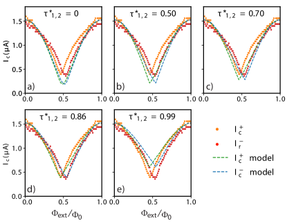
Figure 8 shows a sequence of simulations, blue and green dashed curves, to a set of measurements of (orange) and (red). In all five simulations the critical currents and of the two junctions are taken from the experiment, from Fig. 1c. Since we obtain A and A. In (a) we assume sinusoidal CPRs for both junctions JJ1 and JJ2, and we take the simulated loop inductances into account. Due to the slight asymmetry in loop inductance a small SDE appears. However, this effect is far smaller than what has been measured. Hence, one cannot fit the measurement with the loop inductance asymmetry alone. In (b)-(e) we keep the loop inductances as estimated, but change to non-sinusoidal CPRs by increasing to appreciable values ranging from , indicated in the figures. As before, we obtain the blue and green dashed curves taking the known critical currents and of the two junctions. The best match in this sequence is found for . One can see that the model matches the key features of the experiment very well. However, there are deviations, as seen by the stronger curvature that the measurement points display as compared to the model. The model assumes an almost triangular shape for very large transparencies These differences are yet not understood
Appendix G Conditions for a Diode Effect in a SQUID Device
The following three figures illustrate that an asymmetry is required to obtain a SDE. in Fig. 9(a) and (b) sinusoidal CPRs are assumed. In (a) the loop inductance asymmetry is varied, while the critical-current asymmetry . In contrast, in (b) is varied, while . The loop inductance has been chosen such that the average phase drop over the inductor assumes a large value of . In (c) a SQUID with two single-channel non-sinusoidal CPRs with different transmission probabilities (asymmetry ) are considered, while .
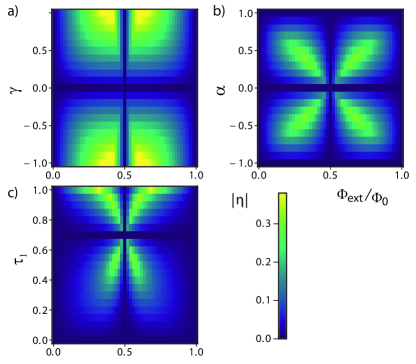
In general, it is seen that the diode efficiency is zero at the symmetry points corresponding in (a) to , in (b) to and in (c) to . Further on, for , , and . For these cases one can show that the CPR of the SQUID is odd in the phase difference . This follows from Eq. 5 and the fact that and are odd functions in . In addition, we note that the position of maximum diode efficiency in flux depends on what kind of asymmetry dominates. It can take up values .
To obtain a SDE in a SQUID loop, an asymmetry is required. This we have illustrated in the previous figure Fig. 9 where out of the three asymmetry parameters , , only one was different from zero. In the following table we show under which conditions the SDE appears depending on all three asymmetry parameters. The table shows that at least one symmetry has to be broken to get the SDE effect. This is a sufficient condition for almost all cases. There is only one exception. It arises for sinusoidal CPRs where a difference in critical currents of the two junctions is not enough for a SDE to appear.
| SDE | |||||
| n.a. | n.a. | no | |||
| n.a. | no | ||||
| n.a. | yes | ||||
| n.a. | n.a. | no | |||
| n.a. | yes | ||||
| n.a. | yes | ||||
| n.a. | no | ||||
| no | |||||
| yes | |||||
| n.a. | yes | ||||
| yes | |||||
| yes | |||||
| n.a. | yes | ||||
| yes | |||||
| yes | |||||
| n.a. | yes | ||||
| yes | |||||
| yes |
References
- Kokkeler et al. [2022] T. H. Kokkeler, A. A. Golubov, and F. S. Bergeret, Field-free anomalous junction and superconducting diode effect in spin-split superconductor/topological insulator junctions, Physical Review B 106, 214504 (2022).
- Zhang et al. [2022] Y. Zhang, Y. Gu, P. Li, J. Hu, and K. Jiang, General theory of josephson diodes, Physical Review X 12, 041013 (2022).
- Josephson [1962] B. Josephson, Possible new effects in superconductive tunnelling, Physics Letters 1, 251 (1962).
- Golubov et al. [2004] A. A. Golubov, M. Y. Kupriyanov, and E. Il’ichev, The current-phase relation in josephson junctions, Reviews of Modern Physics 76, 411 (2004).
- Koops et al. [1996] M. C. Koops, G. V. van Duyneveldt, and R. de Bruyn Ouboter, Direct observation of the current-phase relation of an adjustable superconducting point contact, Physical Review Letters 77, 2542 (1996).
- DellaRocca et al. [2007] M. L. DellaRocca, M. Chauvin, B. Huard, H. Pothier, D. Esteve, and C. Urbina, Measurement of the current-phase relation of superconducting atomic contacts, Physical Review Letters 99, 127005 (2007).
- Buzdin et al. [1982] A. I. Buzdin, L. N. Bulaevskii, and S. V. Panyukov, Critical-current oscillations as a function of the exchange field and thickness of the ferromagnetic metal (f) in an s-f-s josephson junction, JETP Letters 35, 178 (1982).
- Buzdin [2003] A. Buzdin, -junction realization due to tunneling through a thin ferromagnetic layer, JEPT Letters 78, 583 (2003).
- Ryazanov et al. [2001] V. V. Ryazanov, V. A. Oboznov, A. Y. Rusanov, A. V. Veretennikov, A. A. Golubov, and J. Aarts, Coupling of two superconductors through a ferromagnet: Evidence for a junction, Physical Review Letters 86, 2427 (2001).
- Kontos et al. [2002] T. Kontos, M. Aprili, J. Lesueur, F. Genêt, B. Stephanidis, and R. Boursier, Josephson junction through a thin ferromagnetic layer: Negative coupling, Physical Review Letters 89, 137007 (2002).
- Gingrich et al. [2016] E. C. Gingrich, B. M. Niedzielski, J. A. Glick, Y. Wang, D. L. Miller, R. Loloee, W. P. P. Jr, and N. O. Birge, Controllable josephson junctions containing a ferromagnetic spin valve, Nature Physics 12, 564 (2016).
- Sickinger et al. [2012] H. Sickinger, A. Lipman, M. Weides, R. G. Mints, H. Kohlstedt, D. Koelle, R. Kleiner, and E. Goldobin, Experimental evidence of a josephson junction, Physical Review Letters 109, 107002 (2012).
- Krive et al. [2004] I. V. Krive, L. Y. Gorelik, R. I. Shekhter, and M. Jonson, Chiral symmetry breaking and the josephson current in a ballistic superconductor-quantum wire-superconductor junction, Low Temperature Physics 30, 398 (2004).
- Reynoso et al. [2008] A. A. Reynoso, G. Usaj, C. A. Balseiro, D. Feinberg, and M. Avignon, Anomalous josephson current in junctions with spin polarizing quantum point contacts, Physical Review Letters 101, 107001 (2008).
- Buzdin [2008] A. Buzdin, Direct coupling between magnetism and superconducting current in the josephson junction, Physical Review Letters 101, 107005 (2008).
- Zazunov et al. [2009] A. Zazunov, R. Egger, T. Jonckheere, and T. Martin, Anomalous josephson current through a spin-orbit coupled quantum dot, Physical Review Letters 103, 147004 (2009).
- Yokoyama et al. [2013] T. Yokoyama, M. Eto, and Y. V. Nazarov, Josephson current through semiconductor nanowire with spin–orbit interaction in magnetic field, Journal of the Physical Society of Japan 82, 054703 (2013).
- Wakatsuki et al. [2017] R. Wakatsuki, Y. Saito, S. Hoshino, Y. M. Itahashi, T. Ideue, M. Ezawa, Y. Iwasa, and N. Nagaosa, Nonreciprocal charge transport in noncentrosymmetric superconductors, Science Advances 3, 10.1126/sciadv.1602390 (2017).
- Turini et al. [2022] B. Turini, S. Salimian, M. Carrega, A. Iorio, E. Strambini, F. Giazotto, V. Zannier, L. Sorba, and S. Heun, Josephson diode effect in high-mobility insb nanoflags, Nano Letters 22, 10.1021/acs.nanolett.2c02899 (2022).
- Szombati et al. [2016] D. B. Szombati, S. Nadj-Perge, D. Car, S. R. Plissard, E. P. A. M. Bakkers, and L. P. Kouwenhoven, Josephson -junction in nanowire quantum dots, Nature Physics 12, 568 (2016).
- L. et al. [2022] C. B. L., Fuchs, A. Costa, J. J. Pico-Cortes, S. Reinhardt, S. Gronin, G. C. Gardner, T. Lindemann, M. J. Manfra, P. E. F. Junior, D. Kochan, J. J. Fabian, N. Paradiso, and C. Strunk, Effect of rashba and dresselhaus spin-orbit coupling on supercurrent rectification and magnetochiral anisotropy of ballistic josephson junctions, Journal of Physics-Condensed MatterC 34, 10.1088/1361-648X/ac4d5e (2022).
- Rikken et al. [2001] G. L. J. A. Rikken, J. Fölling, and P. Wyder, Electrical magnetochiral anisotropy, Physical Review Letters 87, 236602 (2001).
- Rikken and Wyder [2005] G. L. J. A. Rikken and P. Wyder, Magnetoelectric anisotropy in diffusive transport, Physical Review Letters 94, 016601 (2005).
- Ando et al. [2020] F. Ando, Y. Miyasaka, T. Li, J. Ishizuka, T. Arakawa, Y. Shiota, T. Moriyama, Y. Yanase, and T. Ono, Observation of superconducting diode effect, Nature 584, 373 (2020).
- Daido et al. [2022] A. Daido, Y. Ikeda, and Y. Yanase, Intrinsic superconducting diode effect, Physical Review Letters 128, 037001 (2022).
- Baumgartner et al. [2022] C. Baumgartner, L. Fuchs, A. Costa, S. Reinhardt, S. Gronin, G. C. Gardner, T. Lindemann, M. J. Manfra, P. F. F. Junior, D. Kochan, J. Fabian, N. Paradiso, and C. Strunk, Supercurrent rectification and magnetochiral effects in symmetric josephson junctions, Nature Nanotechnology 17, 39 (2022).
- Bauriedl et al. [2022] L. Bauriedl, C. Bäuml, L. Fuchs, C. Baumgartner, N. Paulik, J. M. Bauer, K.-Q. Lin, J. M. Lupton, T. Taniguchi, K. Watanabe, C. Strunk, and N. Paradiso, Supercurrent diode effect and magnetochiral anisotropy in few-layer nbse2, Nature Communications 13, 10.1038/s41467-022-31954-5 (2022).
- Narita et al. [2022] H. Narita, J. Ishizuka, R. Kawarazaki, D. Kan, Y. Shiota, T. Moriyama, Y. Shimakawa, V. A. Ognev, A. S. Samardak, Y. Yanase, and T. Ono, Field-free superconducting diode effect in noncentrosymmetric superconductor/ferromagnet multilayers, Nature Nanotechnology 17, 823 (2022).
- Jeon et al. [2022] K.-R. Jeon, J.-K. Kim, J. Yoon, J.-C. Jeon, H. Han, A. Cottet, T. Kontos, and S. P. Parkin, Zero-field polarity-reversible josephson supercurrent diodes enabled by a proximity magnetized pt barrier, Nature Materials 21, 1211 (2022).
- Wu et al. [2022] H. Wu, Y. Wang, Y. Xu, P. K. Sivakumar, C. Pasco, U. Filippozzi, S. S. P. Parkin, Y.-J. Zeng, T. McQueen, and M. N. Ali, The field-free josephson diode in a van der waals heterostructure, Nature 604, 653 (2022).
- Lin et al. [2022] J.-X. Lin, P. Siriviboon, H. D. Scammell, S. Liu, D. Rhodes, K. Watanabe, T. Taniguchi, J. Hone, M. S. Scheurer, and J. I. A. Li, Zero-field superconducting diode effect in small-twist-angle trilayer graphene, Nature Phyiscs 18, 1221 (2022).
- Diez-Merida et al. [2023] J. Diez-Merida, A. Diez-Carlon, S. Y. Yang, Y.-M. Xie, X.-J. Gao, J. Senior, K. Watanabe, T. Taniguchi, X. Lu, A. P. Higginbotham, K. T. Law, and D. K. Efetov, Symmetry-broken josephson junctions and superconducting diodes in magic-angle twisted bilayer graphene, Nature Communications 14, 2396 (2023).
- Yuan and Fu [2022] N. F. Q. Yuan and L. Fu, Supercurrent diode effect and finite-momentum superconductors, Proceedings of the National Academy of Sciences of the United States of America 119, 10.1073/pnas.2119548119 (2022).
- Davydova et al. [2022] M. Davydova, S. Prembabu, and L. Fu, Universal josephson diode effect, Science Advances 8, 10.1126/sciadv.abo0309 (2022).
- Suri et al. [2022] D. Suri, A. Kamra, T. N. G. Meier, M. Kronseder, W. Belzig, C. H. Back, and C. Strunk, Non-reciprocity of vortex-limited critical current in conventional superconducting micro-bridges, Applied Physics Letters 121, 102601 (2022).
- Pal et al. [2022] B. Pal, A. Chakraborty, P. K. Sivakumar, M. Davydova, A. K. Gopi, A. K. Pandeya, J. A. Krieger, Y. Zhang, M. Date, S. Ju, N. Yuan, N. B. M. S. L. Fu, and S. S. P. Parkin, Josephson diode effect from cooper pair momentum in a topological semimetal, Nature Physics 18, 1228 (2022).
- Trahms et al. [2023] M. Trahms, L. Melischek, J. F. Steiner, B. Mahendru, I. Tamir, N. Bogdanoff, O. Peters, G. Reecht, C. B. Winkelmann, and F. von Oppenand K. J. Franke, Diode effect in josephson junctions with a single magnetic atom, Nature 615, 628 (2023).
- Chen et al. [2018] C.-Z. Chen, J. J. He, M. N. Ali, G.-H. Lee, K. C. Fong, and K. T. Law, Asymmetric josephson effect in inversion symmetry breaking topological materials, Physical Review B 98, 075430 (2018).
- Kononov et al. [2020] A. Kononov, G. Abulizi, K. Qu, J. Yan, D. Mandrus, K. Watanabe, T. Taniguchi, and C. Schönenberger, One-dimensional edge transport in few-layer wte2, Nano Letters 20, 4228 (2020).
- Legg et al. [2022] H. F. Legg, D. Loss, and J. Klinovaja, Superconducting diode effect due to magnetochiral anisotropy in topological insulators and rashba nanowires, Physical Review B 106, 104501 (2022).
- Cuozzo et al. [2023] J. J. Cuozzo, W. Pan, J. Shabani, and E. Rossi, Microwave-tunable diode effect in asymmetric squids with topological josephson junctions, arXiv:2303.16931 (2023).
- Fulton and Dynes [1970] T. A. Fulton and R. C. Dynes, Current-phase relations in superconducting bridges, Physical Review Letters 25, 794 (1970).
- Fulton et al. [1972] T. A. Fulton, L. N. Dunkleberger, and R. C. Dynes, Quantum interference properties of double josephson junctions, Physical Review B 6, 855 (1972).
- Tsang and Duzer [1975] W.-T. Tsang and T. V. Duzer, dc analysis of parallel arrays of two and three josephson junctions, Journal of Applied Physics 46, 4573 (1975).
- Barone and Paterno [1982] A. Barone and G. Paterno, Physics and Applications of the Josephson Effect (John Wiley & Sons, New York, 1982).
- Buitelaar et al. [2002] M. R. Buitelaar, T. Nussbaumer, and C. Schönenberger, Quantum dot in the kondo regime coupled to superconductors, Physical Review Letters 89, 256801 (2002).
- Doh et al. [2005] Y.-J. Doh, J. A. van Dam, A. L. Roest, E. P. A. M. Bakkers, L. P. Kouwenhoven, and S. D. Franceschi, Tunable supercurrent through semiconductor nanowires, Science 309, 272 (2005).
- Larsen et al. [2015] T. W. Larsen, K. D. Petersson, F. Kuemmeth, T. S. Jespersen, P. Krogstrup, J. Nygård, and C. M. Marcus, Semiconductor-nanowire-based superconducting qubit, Physical Review Letters 115, 127001 (2015).
- Prada et al. [2020] E. Prada, P. San-Jose, M. W. A. de Moor, A. Geresdi, E. J. H. Lee, J. Klinovaja, D. Loss, J. Nygård, R. Aguado, and L. P. Kouwenhoven, From andreev to majorana bound states in hybrid superconductor-semiconductor nanowires, Nature Reviews Physics 2, 575 (2020).
- Burkard et al. [2020] G. Burkard, M. J. Gullans, X. Mi, and J. R. Petta, Superconductor-semiconductor hybrid-circuit quantum electrodynamics, Nature Reviews Physics 2, 129 (2020).
- Souto et al. [2022] R. S. Souto, M. Leijnse, and C. Schrade, Josephson diode effect in supercurrent interferometers, Physical Review Letters 129, 267702 (2022).
- Fominov and S.Mikhailov [2022] Y. V. Fominov and D. S.Mikhailov, Asymmetric higher-harmonic squid as a josephson diode, Physical Review B 106, 134514 (2022).
- Lee et al. [2019] J. S. Lee, B. Shojaei, M. Pendharkar, A. P. McFadden, Y. Kim, H. J. Suominen, M. Kjaergaard, F. Nichele, H. Zhang, C. M. Marcus, and C. J. Palmstrøm, Transport studies of epi-al/inas two-dimensional electron gas systems for required building-blocks in topological superconductor networks, Nano Letters 19, 3083 (2019).
- Nichele et al. [2020] F. Nichele, E. Portolés, A. Fornieri, A. M. Whiticar, A. C. C. Drachmann, S. Gronin, T. Wang, G. C. Gardner, C. Thomas, A. T. Hatke, M. J. Manfra, and C. M. Marcus, Relating andreev bound states and supercurrents in hybrid josephson junctions, Physical Review Letters 124, 226801 (2020).
- Dorokhov [1984] O. Dorokhov, On the coexistence of localized and extended electronic states in the metallic phase, Solid State Communications 51, 381 (1984).
- Nanda et al. [2017] G. Nanda, J. L. Aguilera-Servin, P. Rakyta, A. Kormányos, R. Kleiner, D. Koelle, K. Watanabe, T. Taniguchi, L. M. K. Vandersypen, and S. Goswami, Current-phase relation of ballistic graphene josephson junctions, Nano Letters 17, 3396 (2017).
- Bretheau et al. [2017] L. Bretheau, J. I.-J. Wang, R. Pisoni, K. Watanabe, T. Taniguchi, and P. Jarillo-Herrero, Tunnelling spectroscopy of andreev states in graphene, Nature Physics 13, 756 (2017).
- Manjarrés et al. [2020] D. A. Manjarrés, S. G. Páez, and W. J. Herrera, Skewness and critical current behavior in a graphene josephson junction, Physical Review B 101, 064503 (2020).
- Indolese et al. [2020] D. I. Indolese, P. Karnatak, A. Kononov, R. Delagrange, R. Haller, L. Wang, P. Makk, K. Watanabe, T. Taniguchi, and C. Schönenberger, Compact squid realized in a double-layer graphene heterostructure, Nano Letters 20, 7129 (2020).
- Haller et al. [2022] R. Haller, G. Fülöp, D. Indolese, J. Ridderbos, R. Kraft, L. Y. Cheung, J. H. Ungerer, K. Watanabe, T. Taniguchi, D. Beckmann, R. Danneau, P. Virtanen, and C. Schönenberger, Phase-dependent microwave response of a graphene josephson junction, Physical Review Research 4, 013198 (2022).
- Kulik and Omel’yanchuk [1975] I. O. Kulik and A. N. Omel’yanchuk, Contribution to the microscopic theory of the josephson effect in superconducting bridges, JETP Letters 21, 96 (1975).
- Nazarov [1994] Y. V. Nazarov, Limits of universality in disordered conductors, Physical Review Letters 73, 134 (1994).
- Beenakker [1997] C. W. J. Beenakker, Random-matrix theory of quantum transport, Reviews of Modern Physics 69, 731 (1997).
- Tesche and Clarke [1977] C. D. Tesche and J. Clarke, dc SQUID: Noise and optimization, Journal of Low Temperature Physics 29, 301 (1977).
- Clarke and Braginski [2004] J. Clarke and A. I. Braginski, eds., The SQUID Handbook, Fundamentals and Technology of SQUIDs and SQUID Systems, Vol. I (WILEY-VCH Verlag GmbH, Weinheim, Germany, 2004).
- Granata and Vettoliere [2016] C. Granata and A. Vettoliere, Nano superconducting quantum interference device: A powerful tool for nanoscale investigations, Physics Reports 614, 1 (2016).
- Tosi et al. [2019] L. Tosi, C. Metzger, M. F. Goffman, C. Urbina, H. Pothier, S. Park, A. L. Yeyati, J. Nygard, and P. Krogstrup, Spin-orbit splitting of andreev states revealed by microwave spectroscopy, Physical Review X 9, 011010 (2019).
- Paolucci et al. [2023] F. Paolucci, G. D. Simoni, and F. Giazotto, A gate- and flux-controlled supercurrent diode effect, Applied Physics Letters 122, 042601 (2023).
- Gupta et al. [2023] M. Gupta, G. V. Graziano, M. Pendharkar, J. T. Dong, C. P. Dempsey, C. Palmstrøm, and V. S. Pribiag, Gate-tunable superconducting diode effect in a three-terminal josephson device, Nature Communications 14, 3078 (2023).
- Valentini et al. [2023] M. Valentini, O. Sagi, L. Baghumyan, T. de Gijsel, J. Jung, S. Calcaterra, A. Ballabio, J. A. Servin, K. Aggarwal, M. Janik, T. Adletzberger, R. S. Souto, M. Leijnse, J. Danon, C. Schrade, E. Bakkers, D. Chrastina, G. Isella, and G. Katsaros, Radio frequency driven superconducting diode and parity conserving cooper pair transport in a two-dimensional germanium hole gas, arXiv.2306.07109 (2023).
- Mattis and Bardeen [1958] D. C. Mattis and J. Bardeen, Theory of the anomalous skin effect in normal and superconducting metals, Physical Review 111, 412 (1958).
- Tinkham [2004] M. Tinkham, Introduction to Superconductivity, 2nd ed. (Dover Publications, 2004).
- Annunziata et al. [2010] A. J. Annunziata, D. F. Santavicca, L. Frunzio, G. Catelani, M. J. Rooks, A. Frydman, and D. E. Prober, Tunable superconducting nanoinductors, Nanotechnology 21, 10.1088/0957-4484/21/44/445202 (2010).