Superconducting Pulse Conserving Logic and Josephson-SRAM
Abstract
Superconducting digital Pulse-Conserving Logic (PCL) and Josephson SRAM (JSRAM) memory together enable scalable circuits with energy efficiency 100 beyond leading-node CMOS. Circuit designs support high throughput and low latency when implemented in an advanced fabrication stack with high-critical-current-density Josephson junctions of 1000 A/m2. Pulse-conserving logic produces one single-flux-quantum output for each input, and includes a three-input, three-output gate producing logical or3, majority3 and and3. Gate macros using dual-rail data encoding eliminate inversion latency and produce efficient implementations of all standard logic functions. A full adder using 70 Josephson junctions has a carry-out latency of 5 ps corresponding to an effective 12 levels of logic at 30 GHz. JSRAM (Josephson SRAM) memory uses single-flux-quantum signals throughout an active array to achieve throughput at the same clock rate as the logic. The unit cell has eight Josephson junctions, signal propagation latency of 1 ps, and a footprint of 2 m2. Projected density of JSRAM is 4 MB/cm2, and computational density of pulse-conserving logic is on par with leading node CMOS accounting for power densities and clock rates.
Single Flux Quantum (SFQ) integrated circuits have shown slow-but-steady progress in clock rates, bit-error rates, interconnects, and energy efficiency, with fundamentals established in small-scale demonstrations. The first demonstrations emphasized high data rates, with a binary counter reported at 100 GHz already in 1982 Hamilton and Lloyd (1982). Measurements of Bit Error Rate (BER) show good performance across the SFQ logic families including Rapid-SFQ (RSFQ), Quantum Flux Parametron (QFP), and Reciprocal Quantum Logic (RQL) Herr and Feldman (1996); Herr, Johnson, and Feldman (1999); Herr et al. (2011); Takeuchi, Suzuki, and Yoshikawa (2017); Herr et al. (2022). SFQ logic families operate in the thermal limit, meaning the devices are sized to achieve the desired bit-error rate based on Johnson noise in the Josephson junctions (JJs) at the operating temperature, typically LHe at 4.2 K. Despite the similarities at the gate level, SFQ logic families differ in power distribution and timing characteristics, with widely divergent scalability and performance.
RSFQ has had success in decimation filters for mixed-signal applications Mukhanov et al. (2004); Kashima et al. (2021) where scale is modest and bit rates are high, but scale is limited by a DC current draw of 1 A per 1,000 gates, and by the timing uncertainty of free-running pulses. Energy Efficient SFQ (eSFQ/ERSFQ) Mukhanov (2011); Kirichenko et al. (2019) and Dynamic SFQ (DSFQ) Rylov (2019) variants have these same limitations. Asynchronous approaches Deng et al. (1997); Tzimpragos et al. (2021) can guarantee functional circuits, but at a cost to throughput, as a reduced rate of computation is the only solution to timing uncertainty. Partitioning the circuit onto floating ground planes and “recycling” the current has been proposed to reduce current draw, but the interconnect overheads are high Johnson et al. (2003) and demonstrations limited to 16 partitions with nearest-neighbor interconnect Filippov et al. (2009); Kaplan (2012); Sano et al. (2016). With current recycling, passive transmission line interconnect is unsupported and further scaling is in doubt Semenov and Polyakov (2019).
QFP logic benefits from the scalable power distribution and timing stability that comes from AC bias. In fact, the resonant clock distribution network was first put forward in the context of QFPs Hosoya et al. (1991). Adiabatic QFPs (aQFPs) have switching energy of 10 zJ at a 1 GHz clock rateTakeuchi, Yamanashi, and Yoshikawa (2013); Yamae, Takeuchi, and Yoshikawa (2019), but the advantages of the quasi-adiabatic potential are partially offset by the need for larger junctions, so the energy dissipation for a given BER Takeuchi, Suzuki, and Yoshikawa (2017) is similar to that of RQL Herr et al. (2022). QFPs are used as auxiliary circuits such as qubit readout Volkmann et al. (2015); Grover et al. (2020), where clock rates are low. Demonstrations have advanced to a 4-bit CPU core Ayala et al. (2020), but there is a fundamental limitation in scaling to high performance as the technology supports only one level of logic per clock cycle, translating to high latency and a low logic clock rate. QFPs have high dynamic power dissipation despite low switching energy, as every gate switches every cycle. QFPs do not support transmission line interconnect China et al. (2016).
RQL has stable timing, multiple levels of logic per pipeline stage, low power dissipation and low BER, and low junction count Herr et al. (2011, 2022, 2013). Demonstrations of superconducting transmission line interconnect include synchronous data links chip-to-chip Egan et al. (2022) and isochronous links for going board-to-board Talanov et al. (2022); Dai et al. (2022). Highly functional 8- and 16-bit CPUs have been presented Vesely with AC power distribution at scale Strong et al. (2022). Because SFQ logics are pulse-based, inversion is expensive. The inverting RQL “AnotB” gate Herr et al. (2011) has setup time between the inputs, which adds latency in proportion to the local timing uncertainly despite stable timing on a global scale. Phase Mode Logic (PML) Carmean et al. (2017) encodes logical inversion as a signal-polarity inversion in analogy to CMOS, but the PML data rate is limited to half the resonator clock rate, and inversion has half a cycle of latency.
In this letter we present a new Pulse Conserving Logic (PCL) and Josephson SRAM (JSRAM) memory that have the potential to compete with conventional CMOS in integration scale and performance. These SFQ designs fully exploit the resources of the fabrication process proposed in a companion letter. The fabrication stack and resonant power network apply equally to logic and memory and support up to 400M AC-biased JJs per cm2. Fabrication stack resources were codesigned with the physical layouts of the circuits and carefully balanced to provide dramatic improvements in density relative to legacy designs.
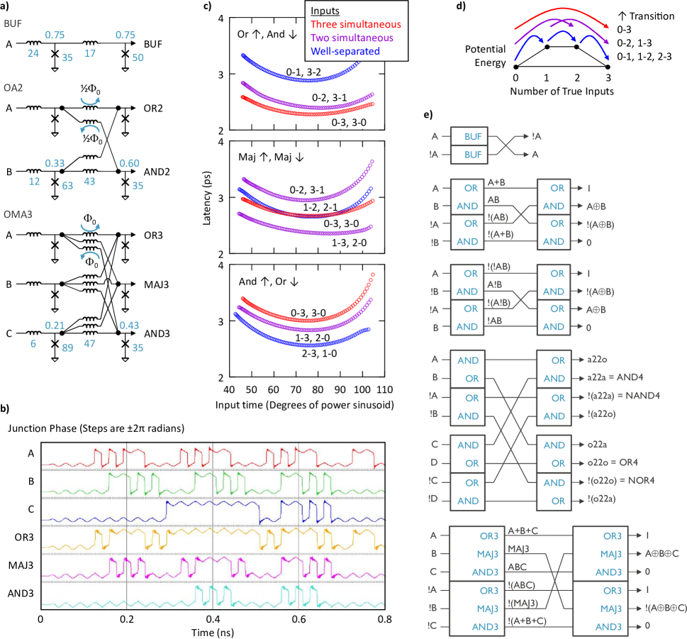
We have developed a new Pulse Conserving Logic (PCL) that uses dual rail signals. Like, CMOS, energy is dissipated only on transitions, and there is no penalty in clock rate or latency for inversion. Our logic gates have the same number of inputs as outputs and preserve pulses, meaning each input SFQ is routed to an output. Gate outputs have symmetric double-well potentials, improving parametric margins and power dissipation. Conservation of pulses enables complex logical functions at reduced latency. The primary set of PCL gates is shown in Fig. 1a. The Josephson Transmission Line (JTL) is a buffer that passes the pulse to a single output while providing isolation and transimpedance gain Likharev and Semenov (1991). The oa2 gate passes the first pulse to an or2 output, and the second pulse to an and2. The three-input, three-output oma3 gate passes the first pulse to o3, the second to maj3 (majority function), and the third to and3. Fanout of the buf is two, and fanout of the oa2 is one-half, meaning a buf stage is required between interconnected gates. Fanout of the oma3 is one-quarter, meaning two buf stages are required between gates, with the second stage sized up by a factor of two.
Compared to an earlier implementation, the oa2 logic gate does not require transformers between the signal inductors Herr et al. (2011) and does not have inductors between outputs or from an output to ground. These advantages permit generalization to oma3. All inputs connect to all outputs, and the applied flux bias on the interconnect distributes the output junctions along a Josephson phase wheel Lee and Ko (1993). Negative inputs pulses to the gates reverse the rotation of the phase wheel. Extension to a four input, four-output gate is thus possible but would require four flux biases and high drive strength on the inputs. To produce the standard logic functions such as or4 and and4, a two-level cascade of two-input gates is more efficient.
As with the other ac powered logics, the SFQ signals are bipolar, with the positive pulse representing a transition to logical “1” and a negative pulse to logical “0”. Waveforms of superconducting phase as shown in Fig. 1b resemble conventional level-based logic. Both low and high levels can persist for multiple clock cycles.
Circuit simulations use a Josephson junction model with nominal critical current, , of 100 A, internal capacitance of 3.5 fH, and voltage gap of 2.75 mV. The bias tap for a standard JTL junction is modeled as sinusoidal voltage source in series with 6.2 fF capacitor. Both capacitors shunt the device, as the bias tap is connected to signal ground, and both scale with device critical current. The junctions are self-shunted, meaning the combined shunt capacitance is low enough that the gap voltage of itself prevents hysteresis in the IV curve. The junction internal resistance has only a secondary effect on switching speed. We include an external shunt resistance, , such that mV this allows voltage sub-gap plasmon oscillations to ring down between SFQ switching events.
Gate delays, shown in Fig. 1c, include the four serial junctions of JTL interconnect needed to connect gate to gate. Latencies are no more than a few ps, but depend strongly on initial state of the gate and the number of simultaneous inputs. Latencies can be understood qualitatively is terms of potential energy as shown in Fig. 1d. In real designs, intermediate pulse timings may occur that are neither well-separated nor simultaneous. The curves in Fig. 1c should be interpreted as the best-case and worst-case timing extremes that envelope possible gate delays.
Dual rail encoding solves the fundamental timing problems of inversion in SFQ pulse-based logics. While global timing is stable as signals travel through the wave pipeline at the rate determined by the ac clock, significant local timing uncertainty arises from thermal noise, parameter spread, and relative pulse arrival time. This translates to latency in SFQ inverting logic due to race conditions. Dual rail inversion is “free” in analogy to CMOS, and enables conventional combinational logic. The cost of duplication in dual rail is partially recouped when mapped onto our PCL gate primitives as the multiple outputs are all available. The dual rail macros, shown in Fig. 1e, produce all the logical functions of a standard CMOS gate library. The XOR3 macro implements a full adder with 70 JJs and carry-out latency of 5 ps corresponding to 12 levels of two-input-gate logic per pipeline stage at 30 GHz. Junction count is about twice the number of transistors in a CMOS implementation Zhuang and Wu (1992).
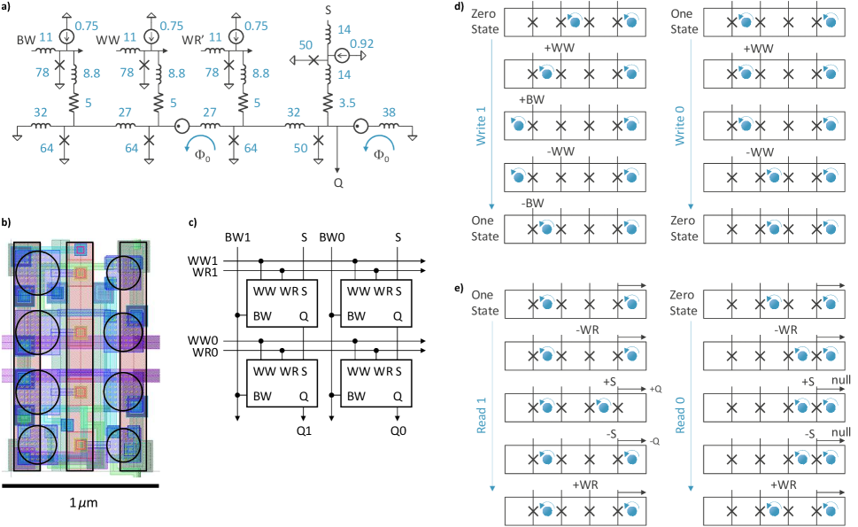
SFQ-compatible memory has historically demonstrated quite modest density despite fundamental SFQ state retention in superconducting loops. The difficulty in scaling superconducting memory centers on the addressing, which requires fanout. Approaches can be categorized as: active, which has the same signal levels and power distribution as logic, i.e. Non-Destructive Read-Out (NDRO) Dorojevets, Bunyk, and Zinoviev (2001); Burnett et al. (2018); passive, meaning the array must be driven with current levels at the perimeter, e.g. Vortex-Transitional Tahara et al. (1989); Nagasawa et al. (1995, 1999); Semenov, Polyakov, and Tolpygo (2019); and magnetic, which requires hysteretic tunnel devices Dayton et al. (2018); Nguyen et al. (2020). Passive and magnetic approaches require drive levels corresponding to 100’s of SFQ pulses, which constrains density, power dissipation, throughput, and latency. Drivers of current must be able to target and tune the levels to accommodate analog addition of word and bit line signals in the unit cell. The Vortex memory has transformers in the unit cell that cannot be miniaturized below 0.25 m with practical drive levels Semenov, Polyakov, and Tolpygo (2019). Magnetic memory devices would require even larger currents to produce the demonstrated switching fields Gingrich et al. (2016); Birge, Madden, and Naaman (2018).
Fig. 2a shows the unit cell of a new Josephson memory, JSRAM, an active array that can be understood as an optimized version of NDRO with about 3 fewer JJs. The unit cell has four JJs for storage and readout of state, and four AC-biased JJs that are JTL-based active address lines. All signals and internal states are SFQ. Resistive coupling to the address lines is used instead of the “escape” junctions used in RSFQ logic. This is feasible as the clock period is long compared to the SFQ pulse width. The current scale in the LR loops is set by the inductance, and the relaxation time is then set by the resistance to small compared to the clock period. Simulated bias current margins of the unit cell embedded in an array exceed 30% for global bias current amplitude.
Physical layout of the unit cell, shown in Fig. 2b, achieves densities for active memory even higher than contemplated for passive arrays. The fabrication stackup proposed in a companion letter enables 4 MB/cm2 density, which represents a 600 increase in density relative to legacy NDRO circuits implemented in a 250 nm Nb fabrication process. Increased density of fabrication resources is achieved across the stack including bias taps, junctions, and inductive wiring. Moving from 250 nm to 50 nm critical dimension in the wiring layers increases inductance density by a factor of 25, and moving to high-kinetic-inductance materials increases density by another 10. The unit cell uses only the first four wiring layers (M1-M4) for inductors, and a single metal layer to implement the two SFQ flux biases, with mutual inductance of 0.5 pH and 4 mA current in the primary. The top two layers are available for passive transmission line wireup across subarrays.
The array, shown in Fig. 2c is wave pipelined with throughput at 30 GHz, making it the functional equivalent of CMOS SRAM. Read and Write operations are illustrated in Fig. 2d. Important features incorporated by the design have been published, including SFQ readout on the bit line Polonsky et al. (1995), and equal-energy levels for the different flux states in the memory cell based on moving an SFQ between superconducting loops Nair and Braiman (2018); Toomey et al. (2019).
| SFQ | TPUv4i | Ratio | |
| Process node | 28 nm | 7 nm | 4 |
| MAC area (m2) | 6,700111Using a derated 50% critical resource utilization relative to JSRAM. | 600222An estimated 10% of the die area dedicated to MAC units. | 11 |
| Clock (GHz) | 30 | 1.05 | 29 |
| Computational density (M op/s/m2) | 4.5 | 1.75 | 2.6 |
| Energy efficiency (op/pJ) | 69333Including a 325 W/W cryocooling overhead. | 3.1 | 22 |
Table 1 compares the size and performance of a PCL bfloat16 multiply-accumulate unit (MAC) to the TPUv4 MAC implemented in leading-node Jouppi et al. (2021). The BF16 multiplier contains an 88 array multiplier for the significand and an 8-bit adder for the exponent, with a small additional overhead for alignment and normalization. The total device count for PCL bf16 MAC is 14,330 JJs, including the systolic array 88 PCL multiplier and the single-precision floating-point 2-bit accumulator. The multiplier contains 49 and2 gates, 7 half-adders, and 42 full-adders for a total of of 4,284 JJs. The single-precision floating-point 32-bit accumulator has 4,163 JJs. The area of the PCL MAC has been estimated by derating JSRAM design density by a factor of two. As shown in the table, power efficiency at the level of on-chip logic is 20 better than CMOS while including a 325 cooling overhead. Computational density of SFQ at 28 nm is higher than 7 nm CMOS, in part due the high clock rate of 30 GHz and in part due to the high utilization of chip real-estate used for logic.
PCL and JSRAM technology enable even higher energy efficiency on the system level, up to 100 due to superconducting interconnect. Low power dissipation of the JSRAM enables efficient chip stacking providing sufficent SRAM-to-compute. Ultimate system performance is determined by capacity and bandiwdth to cryo-DRAM that is an area of active research Ware et al. (2017); Wang et al. (2018); Bae et al. (2019); Lee et al. (2019, 2021); Garzón et al. (2021).
In conclusion, we have put forward advances in SFQ logic and memory design that are essential to scaling. AC-biased PCL logic provides economical dual-rail macros with low-latency inversion, solving one of the central problems of pulse driven logics. JSRAM is a superconducting memory providing SRAM capability and high density. Both technologies are enabled by the high-integration-density fabrication stack described in a companion letter. PCL logic projects to 12 levels of logic per stage with a 30 GHz clock, and a computational density on par with 7 nm CMOS. At the gate level, energy efficiency is 20 better than CMOS including cryocooler efficiency. JSRAM memory projects to 4 MB/cm2 with throughput at the 30 GHz clock rate and a latency of 1 ps per stage in the active array. These technologies enable practical architectures with 100 better power efficiency at the system level and 30 higher clock rate.
Acknowledgements.
Work at imec and imec USA is supported by imec INVEST+ and by Osceola County.Author Contributions
All authors contributed to the work equally.
References
- Hamilton and Lloyd (1982) C. A. Hamilton and F. L. Lloyd, IEEE Electron Device Letters 3, 335 (1982).
- Herr and Feldman (1996) Q. P. Herr and M. J. Feldman, Applied physics letters 69, 694 (1996).
- Herr, Johnson, and Feldman (1999) Q. P. Herr, M. W. Johnson, and M. J. Feldman, IEEE transactions on applied superconductivity 9, 3594 (1999).
- Herr et al. (2011) Q. P. Herr, A. Y. Herr, O. T. Oberg, and A. G. Ioannidis, Journal of applied physics 109, 103903 (2011).
- Takeuchi, Suzuki, and Yoshikawa (2017) N. Takeuchi, H. Suzuki, and N. Yoshikawa, Applied Physics Letters 110, 202601 (2017).
- Herr et al. (2022) Q. Herr, A. Braun, A. Brownfield, E. Rudman, D. Dosch, T. Josephsen, and A. Herr, Superconductor Science and Technology 35, 025017 (2022).
- Mukhanov et al. (2004) O. A. Mukhanov, D. Gupta, A. M. Kadin, and V. K. Semenov, Proceedings of the IEEE 92, 1564 (2004).
- Kashima et al. (2021) R. Kashima, I. Nagaoka, M. Tanaka, T. Yamashita, and A. Fujimaki, IEEE Transactions on Applied Superconductivity 31, 1 (2021).
- Mukhanov (2011) O. A. Mukhanov, IEEE Transactions on Applied Superconductivity 21, 760 (2011).
- Kirichenko et al. (2019) A. F. Kirichenko, I. V. Vernik, M. Y. Kamkar, J. Walter, M. Miller, L. R. Albu, and O. A. Mukhanov, IEEE Transactions on Applied Superconductivity 29, 1 (2019).
- Rylov (2019) S. V. Rylov, IEEE Transactions on Applied Superconductivity 29, 1 (2019).
- Deng et al. (1997) Z. J. Deng, N. Yoshikawa, S. Whiteley, and T. Van Duzer, IEEE transactions on applied superconductivity 7, 3634 (1997).
- Tzimpragos et al. (2021) G. Tzimpragos, J. Volk, D. Vasudevan, N. Tsiskaridze, G. Michelogiannakis, A. Madhavan, J. Shalf, and T. Sherwood, IEEE Micro 41, 71 (2021).
- Johnson et al. (2003) M. W. Johnson, Q. P. Herr, D. J. Durand, and L. A. Abelson, IEEE transactions on applied superconductivity 13, 507 (2003).
- Filippov et al. (2009) T. V. Filippov, A. Sahu, S. Sarwana, D. Gupta, and V. K. Semenov, IEEE transactions on applied superconductivity 19, 580 (2009).
- Kaplan (2012) S. B. Kaplan, IEEE transactions on applied superconductivity 22, 1300103 (2012).
- Sano et al. (2016) K. Sano, T. Shimoda, Y. Abe, Y. Yamanashi, N. Yoshikawa, N. Zen, and M. Ohkubo, IEEE Transactions on Applied Superconductivity 27, 1 (2016).
- Semenov and Polyakov (2019) V. K. Semenov and Y. Polyakov, IEEE Transactions on Applied Superconductivity 29, 1 (2019).
- Hosoya et al. (1991) M. Hosoya, W. Hioe, J. Casas, R. Kamikawai, Y. Harada, Y. Wada, H. Nakane, R. Suda, and E. Goto, IEEE Transactions on Applied Superconductivity 1, 77 (1991).
- Takeuchi, Yamanashi, and Yoshikawa (2013) N. Takeuchi, Y. Yamanashi, and N. Yoshikawa, Applied Physics Letters 102, 052602 (2013).
- Yamae, Takeuchi, and Yoshikawa (2019) T. Yamae, N. Takeuchi, and N. Yoshikawa, Journal of Applied Physics 126, 173903 (2019).
- Volkmann et al. (2015) M. H. Volkmann, L. J. Swenson, P. Spear, B. Bumble, P. K. Day, B. H. Eom, J. D. Whittaker, F. Altomare, A. J. Berkley, A. Kleinsasser, et al., in 2015 15th International Superconductive Electronics Conference (ISEC) (IEEE, 2015) pp. 1–3.
- Grover et al. (2020) J. A. Grover, J. I. Basham, A. Marakov, S. M. Disseler, R. T. Hinkey, M. Khalil, Z. A. Stegen, T. Chamberlin, W. DeGottardi, D. J. Clarke, et al., PRX Quantum 1, 020314 (2020).
- Ayala et al. (2020) C. L. Ayala, T. Tanaka, R. Saito, M. Nozoe, N. Takeuchi, and N. Yoshikawa, IEEE Journal of Solid-State Circuits 56, 1152 (2020).
- China et al. (2016) F. China, N. Tsuji, T. Narama, N. Takeuchi, T. Ortlepp, Y. Yamanashi, and N. Yoshikawa, IEEE Transactions on Applied Superconductivity 27, 1 (2016).
- Herr et al. (2013) A. Y. Herr, Q. P. Herr, O. T. Oberg, O. Naaman, J. X. Przybysz, P. Borodulin, and S. B. Shauck, Journal of Applied Physics 113, 033911 (2013).
- Egan et al. (2022) J. Egan, M. Nielsen, J. Strong, V. Talanov, E. Rudman, B. Song, Q. Herr, and A. Herr, Superconductor Science and Technology 35, 105010 (2022).
- Talanov et al. (2022) V. V. Talanov, D. Knee, D. Harms, K. Perkins, A. Urbanas, J. Egan, Q. Herr, and A. Herr, Superconductor Science and Technology 35, 055011 (2022).
- Dai et al. (2022) H. Dai, C. Kegerreis, D. W. Gamage, J. Egan, M. Nielsen, Y. Chen, D. Tuckerman, S. E. Peek, B. Yelamanchili, M. Hamilton, et al., Superconductor Science and Technology 35, 045014 (2022).
- (30) M. Vesely (Presented at the Applied Superconductivity Conference, Washington State Convention Center, Seattle, WA, October 29, 2018.).
- Strong et al. (2022) J. A. Strong, V. V. Talanov, M. E. Nielsen, A. C. Brownfield, N. Bailey, Q. P. Herr, and A. Y. Herr, Nature Electronics 5, 171 (2022).
- Carmean et al. (2017) D. Carmean, A. Braun, A. Y. Herr, and Q. P. Herr, “Phase-mode based superconducting logic,” (2017), uS Patent 9,543,959.
- Likharev and Semenov (1991) K. K. Likharev and V. K. Semenov, IEEE Transactions on Applied Superconductivity 1, 3 (1991).
- Lee and Ko (1993) G. S. Lee and H. L. Ko, IEEE transactions on applied superconductivity 3, 3001 (1993).
- Zhuang and Wu (1992) N. Zhuang and H. Wu, IEEE journal of solid-state circuits 27, 840 (1992).
- Dorojevets, Bunyk, and Zinoviev (2001) M. Dorojevets, P. Bunyk, and D. Zinoviev, IEEE transactions on applied superconductivity 11, 326 (2001).
- Burnett et al. (2018) R. Burnett, R. Clarke, T. Lee, H. Hearne, J. Vogel, Q. Herr, and A. Herr, in Proceedings of the International Symposium on Memory Systems (2018) pp. 321–323.
- Tahara et al. (1989) S. Tahara, I. Ishida, Y. Ajisawa, and Y. Wada, Journal of applied physics 65, 851 (1989).
- Nagasawa et al. (1995) S. Nagasawa, Y. Hashimoto, H. Numata, and S. Tahara, IEEE Transactions on Applied Superconductivity 5, 2447 (1995).
- Nagasawa et al. (1999) S. Nagasawa, H. Numata, Y. Hashimoto, and S. Tahara, IEEE transactions on applied superconductivity 9, 3708 (1999).
- Semenov, Polyakov, and Tolpygo (2019) V. K. Semenov, Y. A. Polyakov, and S. K. Tolpygo, IEEE Transactions on Applied Superconductivity 29, 1 (2019).
- Dayton et al. (2018) I. M. Dayton, T. Sage, E. C. Gingrich, M. G. Loving, T. F. Ambrose, N. P. Siwak, S. Keebaugh, C. Kirby, D. L. Miller, A. Y. Herr, et al., IEEE Magnetics Letters 9, 1 (2018).
- Nguyen et al. (2020) M.-H. Nguyen, G. J. Ribeill, M. V. Gustafsson, S. Shi, S. V. Aradhya, A. P. Wagner, L. M. Ranzani, L. Zhu, R. Baghdadi, B. Butters, et al., Scientific reports 10, 1 (2020).
- Gingrich et al. (2016) E. Gingrich, B. M. Niedzielski, J. A. Glick, Y. Wang, D. Miller, R. Loloee, W. Pratt Jr, and N. O. Birge, Nature Physics 12, 564 (2016).
- Birge, Madden, and Naaman (2018) N. O. Birge, A. E. Madden, and O. Naaman, in Spintronics XI, Vol. 10732 (SPIE, 2018) pp. 124–134.
- Polonsky et al. (1995) S. Polonsky, A. Kirichenko, V. Semenov, and K. Likharev, IEEE Transactions on Applied Superconductivity 5, 3000 (1995).
- Nair and Braiman (2018) N. Nair and Y. Braiman, Superconductor Science and Technology 31, 115012 (2018).
- Toomey et al. (2019) E. Toomey, M. Onen, M. Colangelo, B. Butters, A. McCaughan, and K. Berggren, Physical review applied 11, 034006 (2019).
- Jouppi et al. (2021) N. P. Jouppi, D. H. Yoon, M. Ashcraft, M. Gottscho, T. B. Jablin, G. Kurian, J. Laudon, S. Li, P. Ma, X. Ma, et al., in 2021 ACM/IEEE 48th Annual International Symposium on Computer Architecture (ISCA) (IEEE, 2021) pp. 1–14.
- Ware et al. (2017) F. Ware, L. Gopalakrishnan, E. Linstadt, S. A. McKee, T. Vogelsang, K. L. Wright, C. Hampel, and G. Bronner, in Proceedings of the International Symposium on Memory Systems (2017) pp. 183–188.
- Wang et al. (2018) F. Wang, T. Vogelsang, B. Haukness, and S. C. Magee, in 2018 IEEE International Memory Workshop (IMW) (IEEE, 2018) pp. 1–4.
- Bae et al. (2019) J.-H. Bae, J.-W. Back, M.-W. Kwon, J. H. Seo, K. Yoo, S. Y. Woo, K. Park, B.-G. Park, and J.-H. Lee, IEEE Electron Device Letters 40, 1614 (2019).
- Lee et al. (2019) G.-h. Lee, D. Min, I. Byun, and J. Kim, in Proceedings of the 46th International Symposium on Computer Architecture (2019) pp. 774–787.
- Lee et al. (2021) G.-H. Lee, S. Na, I. Byun, D. Min, and J. Kim, in 2021 ACM/IEEE 48th Annual International Symposium on Computer Architecture (ISCA) (IEEE, 2021) pp. 637–650.
- Garzón et al. (2021) E. Garzón, Y. Greenblatt, O. Harel, M. Lanuzza, and A. Teman, IEEE Transactions on Very Large Scale Integration (VLSI) Systems (2021).