Programmable Functional Materials Lab, Brain and Consciousness Research Center, Moscow, 121205, Russia
Zero-bias photodetection in 2d materials via geometric design of contacts
Abstract
Structural or crystal asymmetry are necessary conditions for emergence of zero-bias photocurrent in light detectors. Structural asymmetry has been typically achieved via doping being a technologically complex process. Here, we propose an alternative approach to achieve zero-bias photocurrent in 2d material flakes exploiting the geometrical non-equivalence of source and drain contacts. As a prototypical example, we equip a square-shaped flake of PdSe2 with mutually orthogonal metal leads. Upon uniform illumination with linearly-polarized light, the device demonstrates non-zero photocurrent which flips its sign upon 90∘ polarization rotation. The origin of zero-bias photocurrent lies in polarization-dependent lightning-rod effect. It enhances the electromagnetic field at one contact from the orthogonal pair, and selectively activates the internal photoeffect at the respective metal-PdSe2 Schottky junction. The proposed technology of contact engineering can be extended to arbitrary 2d materials and detection of both polarized and natural light.
Keywords: zero-bias detector, contact engineering, lightning-rod effect, polarization sensitivity, IR photodetector, 2d materials
A photodetector should possess some asymmetry or ’preferred direction’ to generate non-zero photocurrent. This stems from the fact that radiation intensity is a scalar, while photocurrent is a vectorial quantity. In the simplest case of photoconductors and bolometers, direct bias current sets such direction. However, this approach suffers from current-induced noise. The bias-free detection, enabling low noise, requires the asymmetry of material crystal lattice or the structure of detector itself. In the latter case, being the most practical, the asymmetric doping of the detector body ( junction) provides the necessary asymmetry.
Two-dimensional materials (2DMs) are expected to enrich the functionalities of light detectors by providing short response times 1, 2, compatibility with silicon waveguides 3 due to atomically thin body, and in-situ tunability of optical properties 4. Implementation of conventional junctions with 2d materials, however, faces technological challenges. Indeed, the technologies of chemical doping for 2DMs are not yet established and inevitably lead to mobility degradation 5, 6. Field-effect doping of 2DMs 7, 8 resolves the mobility issue, but may crop the response times due to extra gate capacitance. Thus, the asymmetry in 2d photodetectors, different from conventional junction, is of high demand.
It has been already noted that a large fraction of photocurrent in 2DM-based detectors is formed at the Schottky junction between the 2d body and metal contacts 9, 10, 11, 12, 13. This occurs both for visible light, where the built-in field separates electron-hole pairs 9, 10, and for long-wavelength radiation where thermoelectric effects and current-voltage nonlinearities take place 12, 13. In a typical detector structure with 2DM placed between identical metals, the photocurrents of two Schottky junctions are exactly compensated, in agreement with symmetry requirements discussed above. Numerous works in the field dealt with contacts of dissimilar metals 9, 12, 14, 15, which, however, requires extra technological steps and careful selection of work functions. If it was possible to ’shadow’ one of the Schottky junctions, the necessary asymmetry would be introduced, and one would get the desired zero-bias low-noise photodetector based on a 2d material.
Here, we show that geometric inequivalence of detector contacts results in the desired ’shadowing’ of one of the Schottky junctions in the near-field, and thus in finite photocurrent at zero bias and uniform illumination. We may suggest similar effects took place in the so-called ’geometric rectifiers’ with non-uniform channel 16, 17, 18, 19, but this possibility was not realized. Alternative attempts to modify the spatial distribution of local fields exploited nano-antennas 20, 21 and gratings 22, 23 placed above the device, which is also challenging technologically. Here, as a practical consequence, we achieve zero-bias polarization-sensitive detection in technologically simple two-terminal structures. The idea is generic and can be applied to arbitrary 2d materials.
For prototypical example, we fabricate and study a detector with rectangular channel and metal contacts to its orthogonal sides. Its operating principle is illustrated in Fig. 1a and its micro-photograph is shown in the inset of Fig.1b, #1.
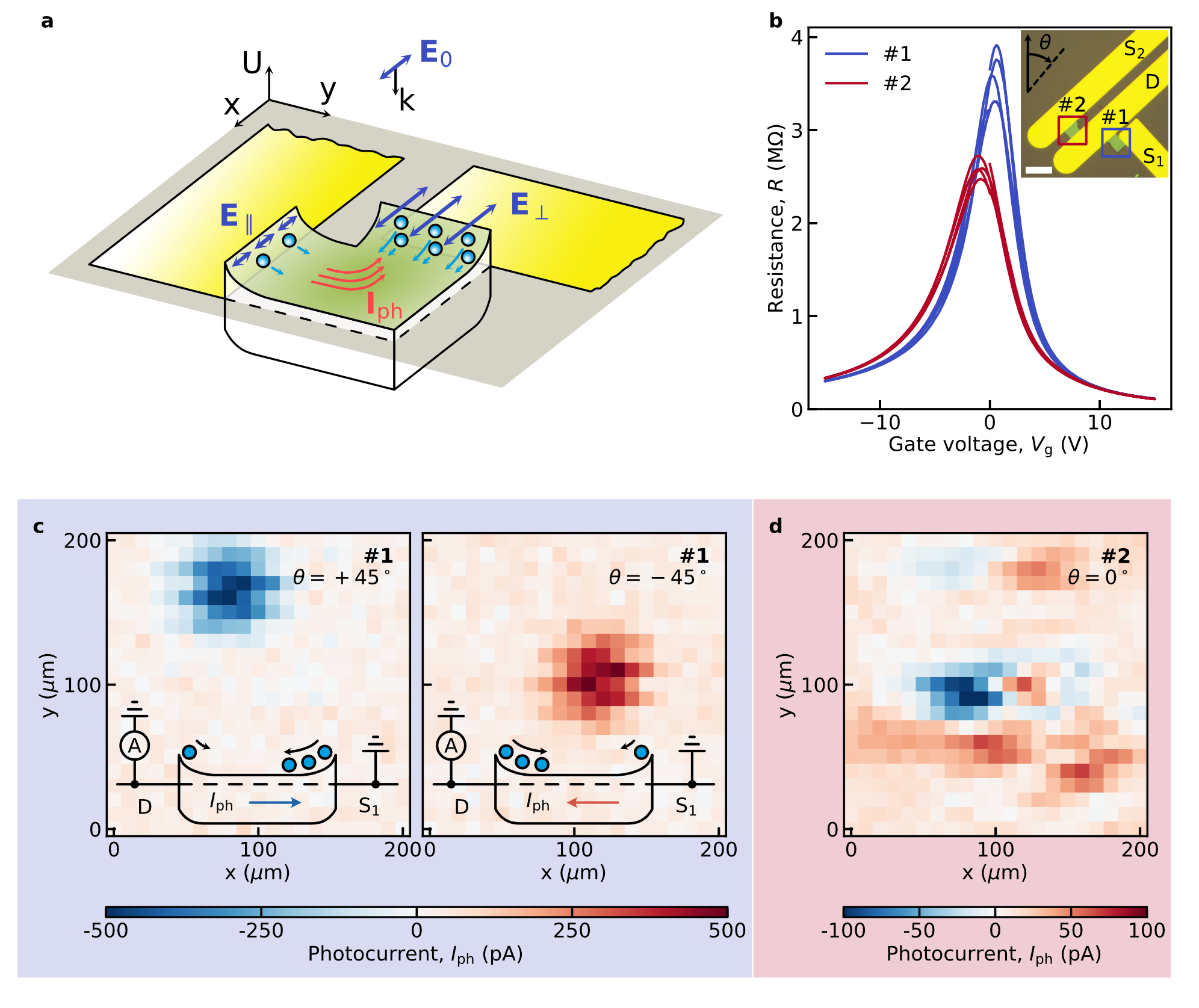
The linearly-polarized radiation with -field orthogonal to one of metal contacts is enhanced locally via to dynamic lightning-rod effect 24, 15. Near another contact, the incident field is suppressed due to dynamic screening currents in metal. As a result, strong photocurrent at the ’electromagnetically active’ Schottky junction is no more compensated by the current at the passive one. Implementation of this idea requires the region of near-field enhancement () to overlap with metal-2DM Schottky junction of typical length nm. Here, we use the mid-infrared illumination with wavelength m, for which this condition is best fulfilled.
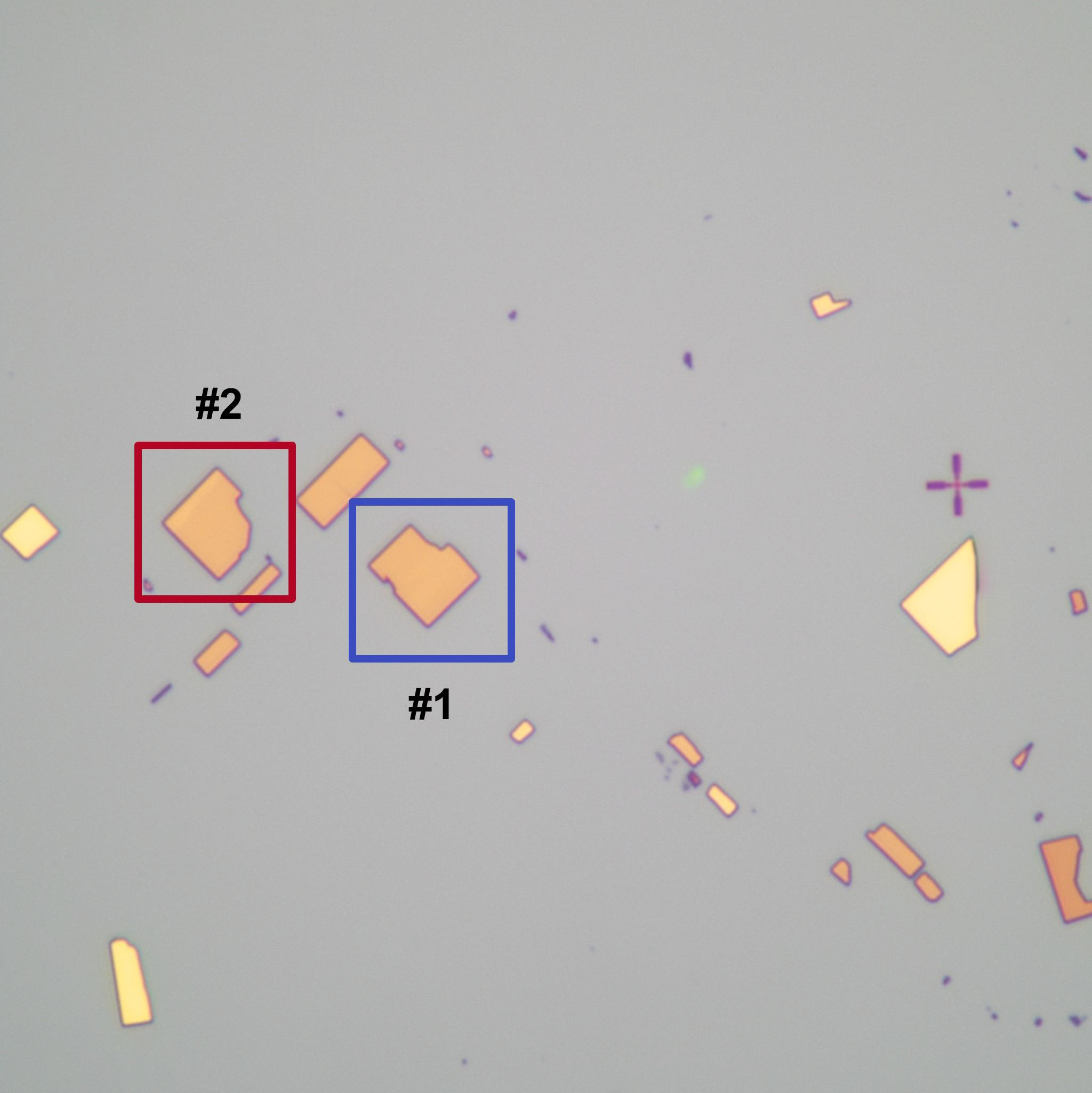
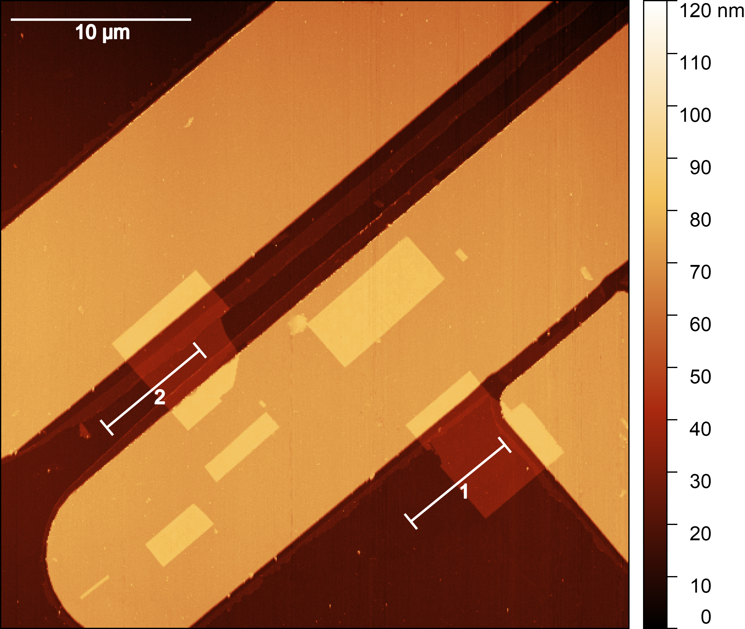
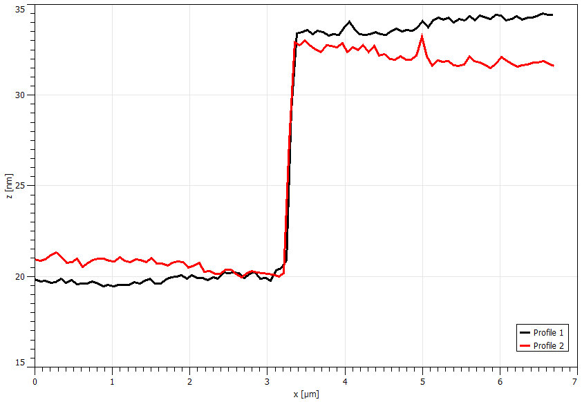
The channel of our corner-type detector is made of quasi two-dimensional PdSe2 [Fig. S1, #1], which already demonstrated strong photoresponse at mid-infrared range 25. The channel thickness is nm [Fig. S2]. The channel size is m2, which is below the wavelength of incident light. A symmetric reference detector #2 was fabricated with the same optical thickness and a comparable channel size m2. The symmetric device has contacts to opposite rectangle sides. Both devices are deposited on a silicon substrate acting as a back gate, covered with 300 nm SiO2 gate dielectric. The devices share the same drain terminal D used for measurements of current and different grounded sources S1 and S2. Two devices have very similar dependencies of resistance on gate voltage , as shown in Fig. 1b.
To prove the suggested operating principle of contact-engineered corner-type device, we present its spatially-resolved photocurrent maps. They were recorded by illuminating the device with linearly polarized, focused beam from IR quantum cascade laser with wavelength m and power mW. Once the radiation polarization is orthogonal to the source S1, one observes a single bright photocurrent spot on the map, as shown in Fig. 1c, left panel. The situation is in stark contrast to our symmetric slit-type detector #2 [Fig. 1d], and to many previous observations 26, 27. There, two nearby photocurrent spots of different sign and reduced magnitude are observed.
Two weak photocurrent spots in nearly-symmetric detectors represent a result of competing current generation events at the source and drain junctions. The light spot covers both terminals in sub-wavelength symmetric detectors, and local intensities at the terminals differ by a small amount, depending on beam position. Once the beam is shifted to the top position in Fig. 1d, the source junction gains slightly larger local intensity, and its photocurrent prevails over the drain. The situation is reverted when shifting the spot downwards to the drain.
We do not observe any traces for secondary photocurrent spot in corner-type device, Fig. 1c, left panel. It implies that one of its contacts (hereby source) generates dominant current independent of the beam position. The maximum photocurrent in corner-type device is nA, which 5x times exceeds the photocurrent at each of two spots for the symmetric slit-type device. Rotation of light polarization by 90∘ results in inversion of photocurrent sign in device #1, as shown in Fig. 1c, right panel. The inversion is explained by the activation of an opposite Schottky junction at the drain via polarization-dependent lightning-rod effect.
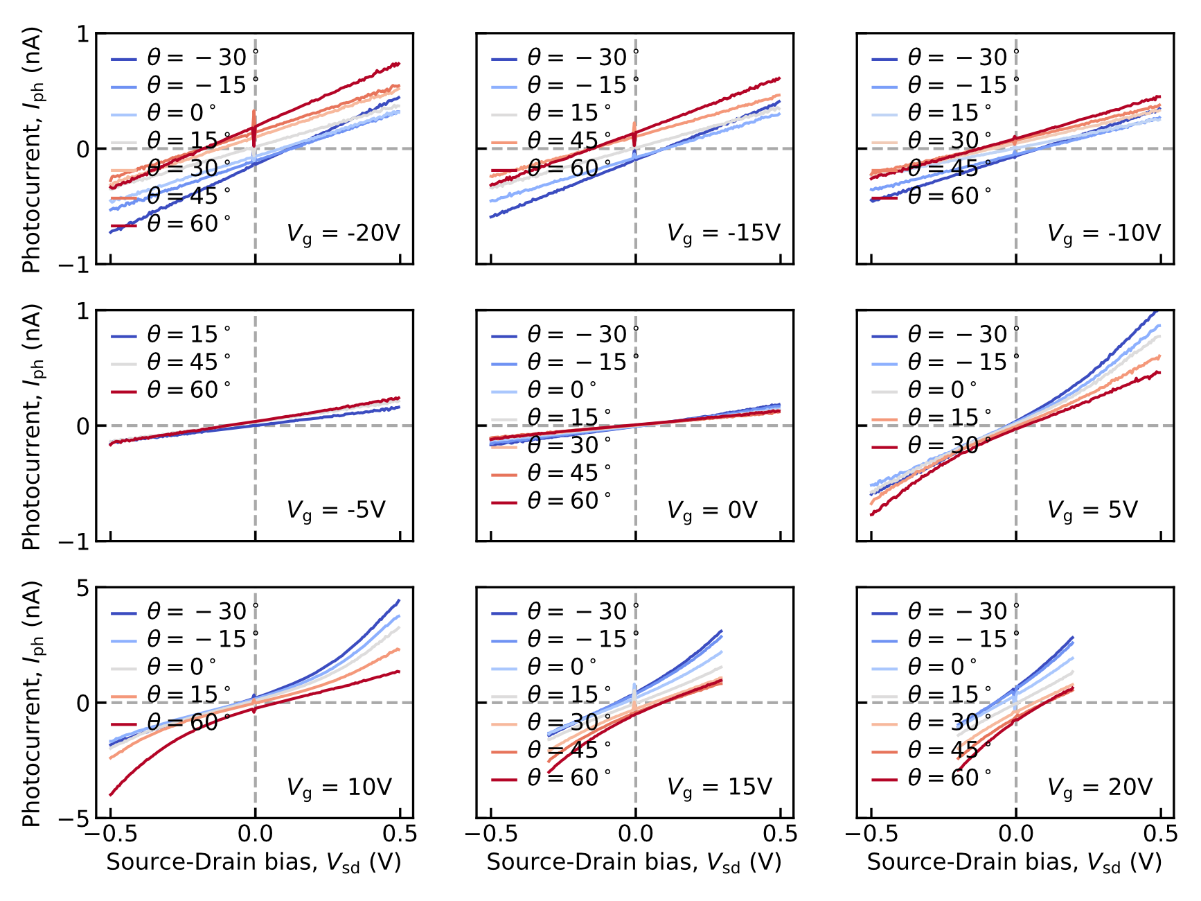
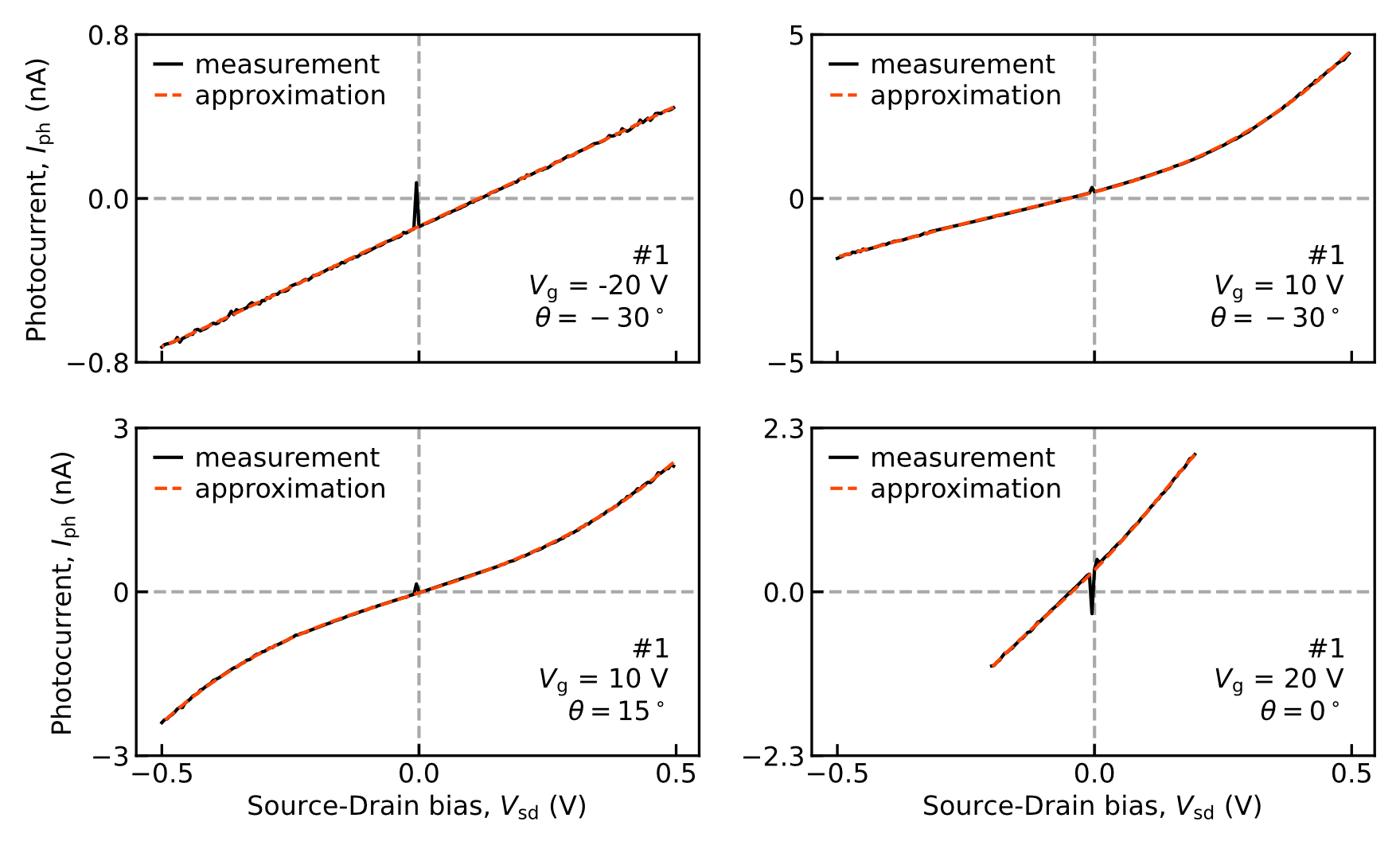
Further confirmations of the suggested operating principle are obtained by recording the dependencies of photocurrent on bias voltage , gate voltage , and polarization angle counted off from the diagonal of square-shaped channel [Fig. S3, S4]. These characteristics are conveniently analyzed by polynominal fits of vs [Fig. S5]:
| (1) |
where is the zero-bias photocurrent, is the photoconductivity, and higher-order terms up to the cubic describe channel nonlinearities.
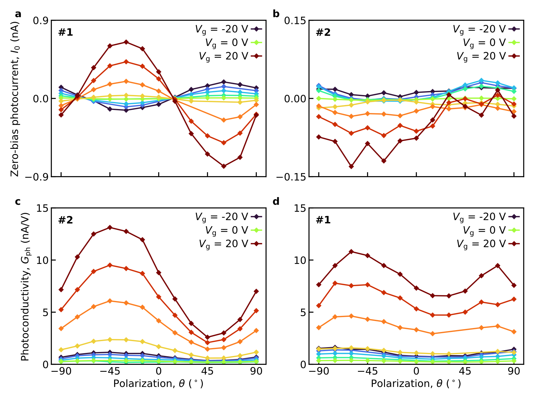
As shown in Fig. 2a, the corner-type device indeed demonstrates a notable zero-bias photocurrent . Its absolute value is maximized and has opposite signs for and . These angles correspond approximately to -field orthogonal to the drain and source contacts, respectively. Interestingly, the non-linearity of photocurrent is polarization-sensitive, and manifests itself for at or for for .
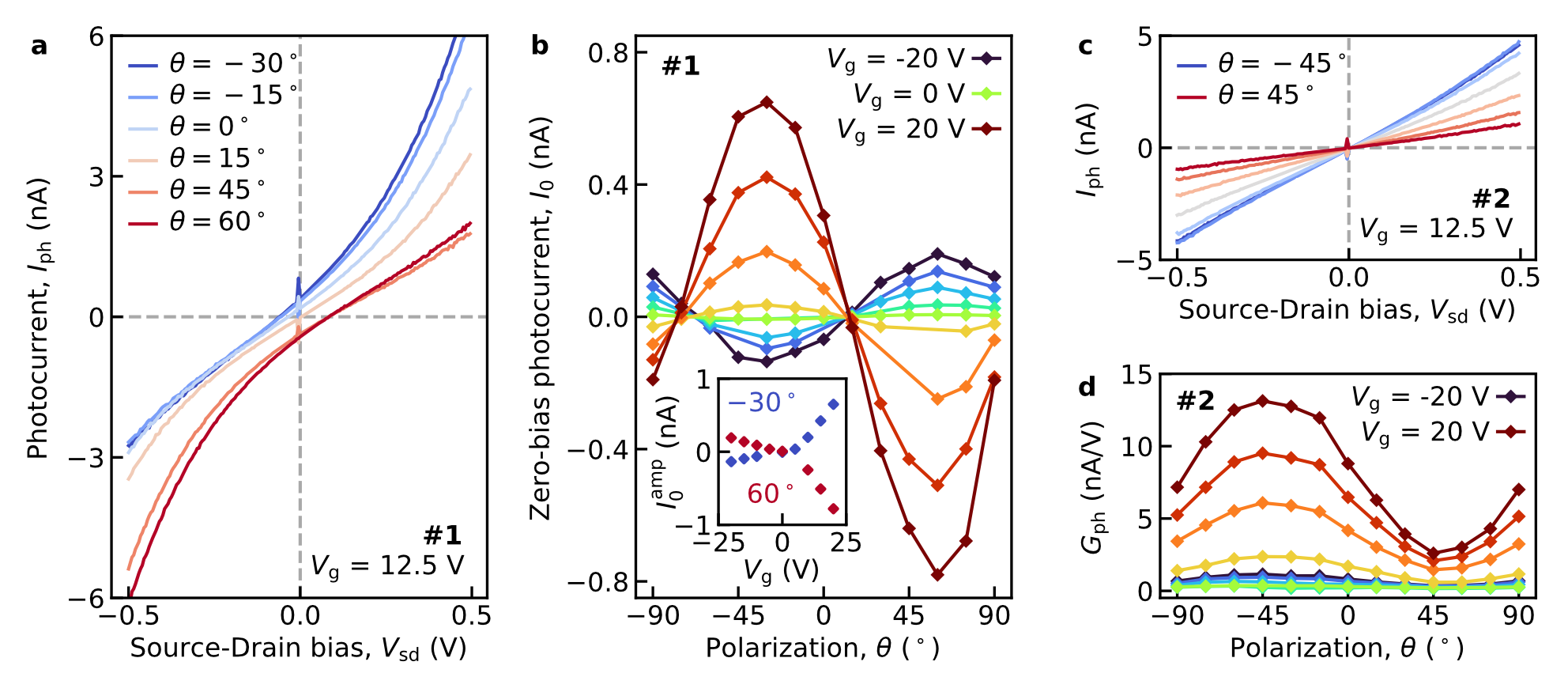
Application of gate voltage considerably modifies the zero-bias current in corner-type device. As seen from Fig. 2b, larger absolute values of result in larger photocurrents, while sign flip of leads to reversal of . The first fact is readily explained by reduced PdSe2 bulk resistance at high carrier density, controlled by [inset of Fig. 2b]. The polarity of is linked to the sign of majority carriers. When the D-terminal of corner-type device is active () and the channel is -doped (), both photocurrent and photovoltage are positive. It implies the motion of photogenerated electrons away from the drain. Such motion can occur upon photovoltaic effect in a band profile shown in the inset of Fig. 1c. The observed sign of zero-bias current can be alternatively explained by thermal diffusion of majority carriers from ’hot’ contact to the ’cold’ bulk. Discrimination between photovoltaic and thermoelectric scenarios requires more careful determination of PdSe2 band gap 28.
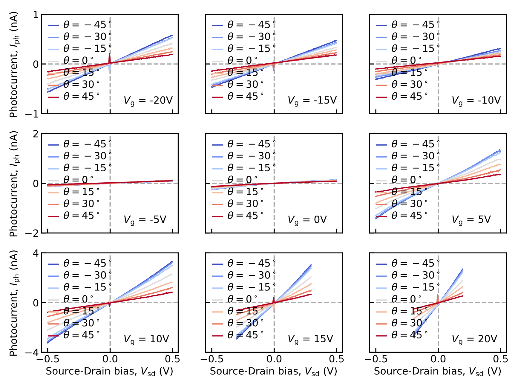
Similar measurements and data processing were performed for the symmetric slit-type detector #2. The dependencies of photocurrent on bias voltage and polarization angle hereby show a completely different qualitative behavior [Fig. 2c]. The zero-bias photocurrent is absent (least for centered illumination) and the dependencies are almost linear. The photoconductivity of the symmetric device, shown in Fig. 2d, displays strong, approximately three-fold, variation with polarization angle. It is maximized for -field perpendicular to metal contacts, and drops to minimum upon polarization rotation. Again, these observations are explained by lightning-rod effect at the metal contacts. Indeed, the photoconductivity is maximized at maximum local field in the channel, which occurs precisely for -field orthogonal to the contacts. The sign of photoconductivity in our measurements is positive, which hints on the possibility of interband electron-hole generation.
We complete our discussion of contact-engineered detectors by presenting the simulation results for local electromagnetic fields. This enables us not only to prove the suggested physics of polarization-dependent lightning-rod effect, but also to indicate possible optimization directions (see Methods for technical details).
The simulation of local field distribution under plane-wave linearly polarized illumination [Fig. 3c,d] confirms strong field enhancement near one metal pad and its suppression near another. Approaching the ’active pad’, the field diverges as inverse square root of distance. At shortest distances, it saturates to finite value inversely proportional to 2d material conductivity. An interesting feature seen in simulations is oscillation of local field intensity along the channel indicating that resonant effects in PdSe2 flake may affect the photoresponse.
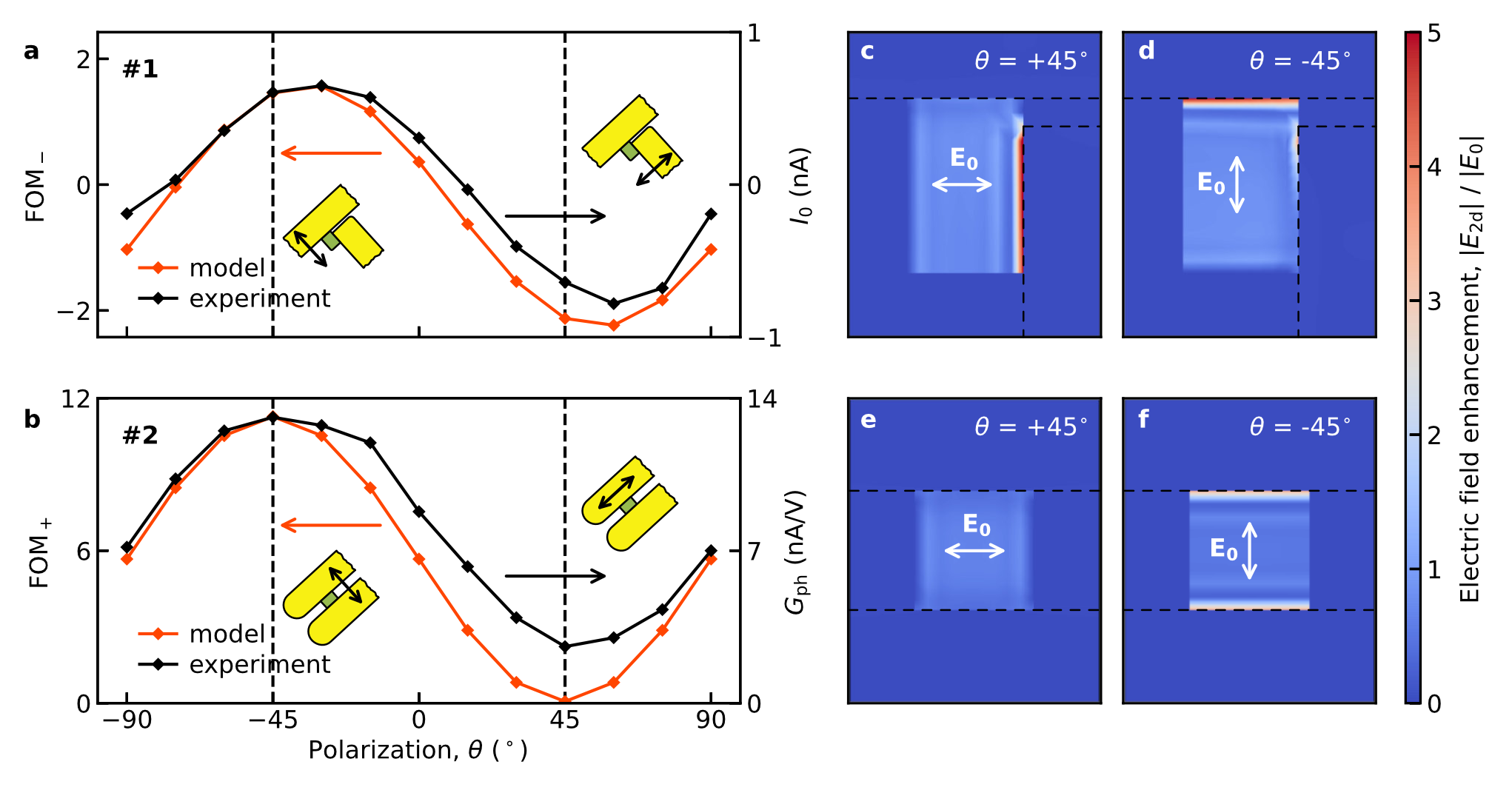
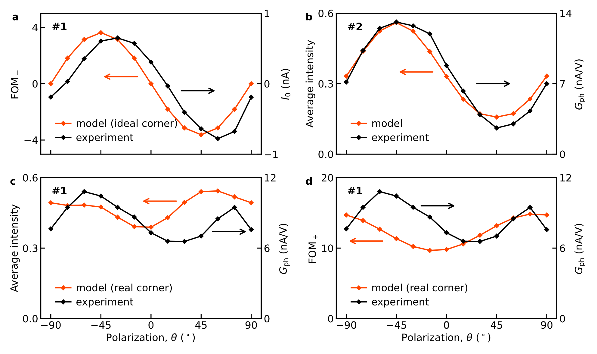
A perfect asymmetrically engineered detector should have very small local field at one contact, and large field at another one. It is also natural to require local field enhancement in a well-designed device, compared to the incident field . Based on these arguments, we choose the electromagnetic figure of merit for asymmetric device (FOM-) as the difference of average local intensities at source and drain, and , normalized by the incident field intensity :
| (2) |
Averaging is performed along the length of contact, while the distance between metal pad and the point where field is calculated is taken to be 100 nm, an approximate width of the Schottky junction 29.
We expect that FOM- given above, Eq. (2), serves as a measure of zero-bias current independent of particular detection physics. Particularly, it measures the difference between numbers of electron-hole pairs generated at two Schottky junctions in the case of internal photovoltaic effect 30. It is also proportional to the difference in electron temperatures at the two junctions, which is proportional to photocurrent if photothermoelectric effect takes place 31. In any case, the proportionality between FOM- and photocurrent indeed experimentally holds. We show it in Fig. 3a by comparing the computed FOM (orange line) and the measured zero-bias photocurrent (black line). These quantities coincide well up to a dimensional multiplier. The simulation captures well the tiny details of experiment. Particularly, the maxima of FOM- and photocurrent appear not exactly for -field orthogonal to the contacts, but are shifted by from the expected position. This feature stems from deviations of detector structure from perfectly symmetric square PdSe2 channel [Fig. S7a].
The polarization dependence of photocurrent in a symmetric device is governed by the same vectorial lightning-rod effect, though the signal emerges only at finite bias. The photoconductivity of the symmetric device should be proportional to the absorbed power at the Schottky junctions, and, in turn, to the quantity As shown in Fig. 3b, the simulated FOM matches well the measured photoconductivity. The agreement becomes even better if we compute the electromagnetic power absorbed in the whole PdSe2 channel, not only at its contacts [Fig. S7b].
In conclusion, we have shown that geometric engineering of contacts to 2d materials provides a unique opportunity to achieve zero-bias photodetection with low noise. The technique applies to arbitrary 2d materials and is readily scalable to arbitrary wavelengths. The only requirement for achievement of appreciable photosignal is the presence of rectifying Schottky junction at metal-2d semiconductor contact, which is the case unless the ohmic contact is fabricated intentionally 32. The physics of photocurrent generation at the junction, again, can be arbitrary. It may include but not limited to photovoltaic, photothermoelectric effects and direct rectification by junction -nonlinearities.
It is important that the demonstrated pair of photodetectors is able to resolve the linear polarization state of the incident light 20. Namely, by normalizing the signal of corner-type detector to the signal of slit-type one, one gets rid of photocurrent dependence on light power. The dependence of normalized current on can be recorded once and further used for unambiguous determination of polarization angle within the -range. Already the sign of photocurrent in corner-type device tells us unambiguously which quadrant the polarization angle belongs to. This property can be important for optical communications using two independent orthogonal polarization channels for increased bit capacitance.
An arbitrary geometric inequivalence of two contacts to 2d channel should result in finite zero-bias photocurrent 16, 19. To make this photocurrent large, the inequivalence should be strong. We have shown that it can be quantitatively characterized by the figure of merit (2) being the ratio of local intensity difference at the two contacts, normalized by intensity of the incident light. In the proposed design with orthogonal source and drain contacts, the numerical value of FOM- is moderate and reaches in absolute value. Yet, there are no fundamental limitations to this quantity. According to our simulations, further seven-fold enhancement of FOM- is possible upon optimization of contacts’ width and SiO2 thickness (see Supporting Information, Section IV).
We have shown that a versatile tool to achieve electromagnetically inequivalent contacts lies in exploiting polarization-dependent field enhancement by keen metal edges 24, 15. Such effect may be even more pronounced for contacts with in-plane patterning, which may have either regular (e.g. sawtooth) or fractal 33 shape. Another option toward electromagnetic asymmetry may rely on optical resonance in one metal pad and anti-resonance in another. Optimized shapes of metal contacts can be accessed with machine-learning techniques 34. To conclude, the technique of geometrically dissimilar contacts to 2d materials open wide opportunities in low-noise zero-bias detection with possible option of polarization resolution.
Methods. PdSe2 flakes were prepared by micro-mechanical cleavage of the bulk crystal and deposited on lightly doped SiO2/Si substrate [Fig. S1]. Their thickness nm was verified using atomic force microscopy [Fig. S2]. Top contacts to PdSe2 were achieved by magnetron sputtering of Ti/Au (3/60 nm).
Optical measurements were performed in evacuated chamber with residual gas pressure Torr. The radiation was fed from quantum cascade laser (QCL) with central wavelength m. A -waveplate with axes rotated by to initial polarization direction of laser radiation and a polarizer were introduced between laser and sample. This enabled power-preserving polarization rotation in our experiment. We used internal modulation of QCL current with Hz, which enabled lock-in measurements of the photocurrent.
Simulations were performed in a CST Microwave studio package using finite-element method at a single frequency. Metal contacts and PdSe2 flake were treated as infinitely thin (sheet) conductors with areal impedances and , respectively, where Ohm is the free-space impedance. The definite value of PdSe2 impedance does not affect the shape of FOM dependence as soon as . The latter fact simply implies that absorbance by extended PdSe2 film is much less than unity, which is an experimentally established fact 35. Wavelength-dependent dielectric constants SiO2 for simulations were used from Ref. 36.
Data Availability Statement
The data that support the findings of this study are available from the corresponding author upon reasonable request.
Supporting Information
(I) Devices fabrication and characterization, (II) Photocurrent measurement details, (III) Simulation details, (IV) Optimization of corner-type detector (PDF)
Acknowledgments
This work was supported by the Russian Science Foundation (Grant No. 21-72-00078). The devices were fabricated using the equipment of the Center of Shared Research Facilities (Moscow Institute of Physics and Technology). We are grateful to V.V. Dremov for experimental assistance.
Author Contributions
D.S. conceived and supervised the project. V.S and D.M performed transport and photoresponse measurements. V.S and D.S analyzed experimental data. A.S. and D.S. developed theoretical model and performed simulations. M.K and I.D. fabricated devices. S.Z. assisted in tuning of optical setups. V.S. and D.S. wrote the manuscript, with input from all the co-authors. All authors contributed to the discussions.
Competing interests
The authors declare no competing financial interest.
References
- Xia et al. 2009 Xia, F.; Mueller, T.; Lin, Y. M.; Valdes-Garcia, A.; Avouris, P. Ultrafast graphene photodetector. Nature Nanotechnology 2009, 4, 839–843
- Massicotte et al. 2016 Massicotte, M.; Schmidt, P.; Vialla, F.; Schädler, K. G.; Reserbat-Plantey, A.; Watanabe, K.; Taniguchi, T.; Tielrooij, K. J.; Koppens, F. H. L. Picosecond photoresponse in van der Waals heterostructures. Nature Nanotechnology 2016, 11, 42–46
- Gan et al. 2013 Gan, X.; Shiue, R.-J.; Gao, Y.; Meric, I.; Heinz, T. F.; Shepard, K.; Hone, J.; Assefa, S.; Englund, D. Chip-integrated ultrafast graphene photodetector with high responsivity. Nature Photonics 2013, 7, 883–887
- Ren et al. 2012 Ren, L.; Zhang, Q.; Yao, J.; Sun, Z.; Kaneko, R.; Yan, Z.; Nanot, S.; Jin, Z.; Kawayama, I.; Tonouchi, M.; Tour, J. M.; Kono, J. Terahertz and infrared spectroscopy of gated large-area graphene. Nano Letters 2012, 12, 3711–3715
- Liu et al. 2014 Liu, N.; Tian, H.; Schwartz, G.; Tok, J. B.-H.; Ren, T.-L.; Bao, Z. Large-Area, Transparent, and Flexible Infrared Photodetector Fabricated Using P-N Junctions Formed by N-Doping Chemical Vapor Deposition Grown Graphene. Nano Letters 2014, 14, 3702–3708
- Wang et al. 2018 Wang, G. et al. Seamless lateral graphene p–n junctions formed by selective in situ doping for high-performance photodetectors. Nature Communications 2018, 9, 5168
- Castilla et al. 2019 Castilla, S.; Terrés, B.; Autore, M.; Viti, L.; Li, J.; Nikitin, A. Y.; Vangelidis, I.; Watanabe, K.; Taniguchi, T.; Lidorikis, E.; Vitiello, M. S.; Hillenbrand, R.; Tielrooij, K. J.; Koppens, F. H. Fast and Sensitive Terahertz Detection Using an Antenna-Integrated Graphene pn Junction. Nano Letters 2019, 19, 2765–2773
- Mylnikov et al. 2023 Mylnikov, D. A.; Titova, E. I.; Kashchenko, M. A.; Safonov, I. V.; Zhukov, S. S.; Semkin, V. A.; Novoselov, K. S.; Bandurin, D. A.; Svintsov, D. A. Terahertz Photoconductivity in Bilayer Graphene Transistors: Evidence for Tunneling at Gate-Induced Junctions. Nano Letters 2023, 23, 220–226
- Mueller et al. 2010 Mueller, T.; Xia, F.; Avouris, P. Graphene photodetectors for high-speed optical communications. Nature Photonics 2010, 4, 297–301
- Echtermeyer et al. 2014 Echtermeyer, T. J.; Nene, P. S.; Trushin, M.; Gorbachev, R. V.; Eiden, A. L.; Milana, S.; Sun, Z.; Schliemann, J.; Lidorikis, E.; Novoselov, K. S.; Ferrari, A. C. Photothermoelectric and Photoelectric Contributions to Light Detection in Metal–Graphene–Metal Photodetectors. Nano Letters 2014, 14, 3733–3742
- Tielrooij et al. 2015 Tielrooij, K. J.; Massicotte, M.; Piatkowski, L.; Woessner, A.; Ma, Q.; Jarillo-Herrero, P.; van Hulst, N. F.; Koppens, F. H. L. Hot-carrier photocurrent effects at graphene–metal interfaces. Journal of Physics: Condensed Matter 2015, 27, 164207
- Cai et al. 2014 Cai, X.; Sushkov, A. B.; Suess, R. J.; Jadidi, M. M.; Jenkins, G. S.; Nyakiti, L. O.; Myers-Ward, R. L.; Li, S.; Yan, J.; Gaskill, D. K.; Murphy, T. E.; Drew, H. D.; Fuhrer, M. S. Sensitive room-temperature terahertz detection via the photothermoelectric effect in graphene. Nature Nanotechnology 2014, 9, 814–819
- Bandurin et al. 2018 Bandurin, D. A.; Gayduchenko, I.; Cao, Y.; Moskotin, M.; Principi, A.; Grigorieva, I. V.; Goltsman, G.; Fedorov, G.; Svintsov, D. Dual origin of room temperature sub-terahertz photoresponse in graphene field effect transistors. Applied Physics Letters 2018, 112, 141101
- Gayduchenko et al. 2018 Gayduchenko, I. A.; Fedorov, G. E.; Moskotin, M. V.; Yagodkin, D. I.; Seliverstov, S. V.; Goltsman, G. N.; Yu Kuntsevich, A.; Rybin, M. G.; Obraztsova, E. D.; Leiman, V. G.; Shur, M. S.; Otsuji, T.; Ryzhii, V. I. Manifestation of plasmonic response in the detection of sub-terahertz radiation by graphene-based devices. Nanotechnology 2018, 29, 245204
- Semkin et al. 2022 Semkin, V.; Mylnikov, D.; Titova, E.; Zhukov, S.; Svintsov, D. Gate-controlled polarization-resolving mid-infrared detection at metal–graphene junctions. Applied Physics Letters 2022, 120, 191107
- Zhou et al. 2018 Zhou, C.; Raju, S.; Li, B.; Chan, M.; Chai, Y.; Yang, C. Y. Self-Driven Metal–Semiconductor–Metal WSe2 Photodetector with Asymmetric Contact Geometries. Advanced Functional Materials 2018, 28, 1802954
- Auton et al. 2017 Auton, G.; But, D. B.; Zhang, J.; Hill, E.; Coquillat, D.; Consejo, C.; Nouvel, P.; Knap, W.; Varani, L.; Teppe, F.; Torres, J.; Song, A. Terahertz Detection and Imaging Using Graphene Ballistic Rectifiers. Nano Letters 2017, 17, 7015–7020
- Brownless et al. 2020 Brownless, J.; Zhang, J.; Song, A. Graphene ballistic rectifiers: Theory and geometry dependence. Carbon 2020, 168, 201–208
- Chen et al. 2022 Chen, J.; Zhang, Z.; Feng, J.; Xie, X.; Jian, A.; Li, Y.; Guo, H.; Zhu, Y.; Li, Z.; Dong, J.; Cui, Q.; Shi, Z.; Xu, C. 2D InSe Self-Powered Schottky Photodetector with the Same Metal in Asymmetric Contacts. Advanced Materials Interfaces 2022, 9, 2200075
- Wei et al. 2020 Wei, J.; Li, Y.; Wang, L.; Liao, W.; Dong, B.; Xu, C.; Zhu, C.; Ang, K.-W.; Qiu, C.-W.; Lee, C. Zero-bias mid-infrared graphene photodetectors with bulk photoresponse and calibration-free polarization detection. Nature Communications 2020, 11, 6404
- Wei et al. 2021 Wei, J.; Xu, C.; Dong, B.; Qiu, C.-W.; Lee, C. Mid-infrared semimetal polarization detectors with configurable polarity transition. Nature Photonics 2021, 15, 614–621
- Popov et al. 2015 Popov, V. V.; Fateev, D. V.; Ivchenko, E. L.; Ganichev, S. D. Noncentrosymmetric plasmon modes and giant terahertz photocurrent in a two-dimensional plasmonic crystal. Phys. Rev. B 2015, 91, 235436
- Yahniuk et al. 2022 Yahniuk, I.; Budkin, G. V.; Kazakov, A.; Otteneder, M.; Ziegler, J.; Weiss, D.; Mikhailov, N. N.; Dvoretskii, S. A.; Wojciechowski, T.; Bel’kov, V. V.; Knap, W.; Ganichev, S. D. Terahertz Ratchet Effect in Interdigitated HgTe Structures. Phys. Rev. Appl. 2022, 18, 054011
- Nikulin et al. 2021 Nikulin, E.; Mylnikov, D.; Bandurin, D.; Svintsov, D. Edge diffraction, plasmon launching, and universal absorption enhancement in two-dimensional junctions. Physical Review B 2021, 103, 085306
- Long et al. 2019 Long, M.; Wang, Y.; Wang, P.; Zhou, X.; Xia, H.; Luo, C.; Huang, S.; Zhang, G.; Yan, H.; Fan, Z.; Wu, X.; Chen, X.; Lu, W.; Hu, W. Palladium Diselenide Long-Wavelength Infrared Photodetector with High Sensitivity and Stability. ACS Nano 2019,
- Lemme et al. 2011 Lemme, M. C.; Koppens, F. H. L.; Falk, A. L.; Rudner, M. S.; Park, H.; Levitov, L. S.; Marcus, C. M. Gate-Activated Photoresponse in a Graphene p–n Junction. Nano Letters 2011, 11, 4134–4137
- Badioli et al. 2014 Badioli, M.; Woessner, A.; Tielrooij, K. J.; Nanot, S.; Navickaite, G.; Stauber, T.; García De Abajo, F. J.; Koppens, F. H. Phonon-mediated mid-infrared photoresponse of graphene. Nano Letters 2014, 14, 6374–6381
- Nishiyama et al. 2022 Nishiyama, W.; Nishimura, T.; Nishioka, M.; Ueno, K.; Iwamoto, S.; Nagashio, K. Is the Bandgap of Bulk PdSe2 Located Truly in the Far-Infrared Region Determination by Fourier-Transform Photocurrent Spectroscopy. Advanced Photonics Research 2022, 3, 2200231
- Lee et al. 2008 Lee, E. J.; Balasubramanian, K.; Weitz, R. T.; Burghard, M.; Kern, K. Contact and edge effects in graphene devices. Nature Nanotechnology 2008, 3, 486–490
- Afzal et al. 2020 Afzal, A. M.; Dastgeer, G.; Iqbal, M. Z.; Gautam, P.; Faisal, M. M. High-Performance p-BP/n-PdSe2 Near-Infrared Photodiodes with a Fast and Gate-Tunable Photoresponse. ACS Applied Materials & Interfaces 2020, 12, 19625–19634
- Dai et al. 2020 Dai, M.; Chen, H.; Wang, F.; Long, M.; Shang, H.; Hu, Y.; Li, W.; Ge, C.; Zhang, J.; Zhai, T.; Fu, Y.; Hu, P. Ultrafast and Sensitive Self-Powered Photodetector Featuring Self-Limited Depletion Region and Fully Depleted Channel with van der Waals Contacts. ACS Nano 2020, 14, 9098–9106
- Schulman et al. 2018 Schulman, D. S.; Arnold, A. J.; Das, S. Contact engineering for 2D materials and devices. Chem. Soc. Rev. 2018, 47, 3037–3058
- De Nicola et al. 2018 De Nicola, F.; Puthiya Purayil, N. S.; Spirito, D.; Miscuglio, M.; Tantussi, F.; Tomadin, A.; De Angelis, F.; Polini, M.; Krahne, R.; Pellegrini, V. Multiband Plasmonic Sierpinski Carpet Fractal Antennas. ACS Photonics 2018, 5, 2418–2425
- Campbell et al. 2019 Campbell, S. D.; Sell, D.; Jenkins, R. P.; Whiting, E. B.; Fan, J. A.; Werner, D. H. Review of numerical optimization techniques for meta-device design [Invited]. Optical Materials Express 2019, 9, 1842
- Ermolaev et al. 2021 Ermolaev, G. A.; Voronin, K. V.; Tatmyshevskiy, M. K.; Mazitov, A. B.; Slavich, A. S.; Yakubovsky, D. I.; Tselin, A. P.; Mironov, M. S.; Romanov, R. I.; Markeev, A. M.; Kruglov, I. A.; Novikov, S. M.; Vyshnevyy, A. A.; Arsenin, A. V.; Volkov, V. S. Broadband Optical Properties of Atomically Thin PtS2 and PtSe2. Nanomaterials 2021, 11, 3269
- Kischkat et al. 2012 Kischkat, J.; Peters, S.; Gruska, B.; Semtsiv, M.; Chashnikova, M.; Klinkmüller, M.; Fedosenko, O.; Machulik, S.; Aleksandrova, A.; Monastyrskyi, G.; Flores, Y.; Masselink, W. T. Mid-infrared optical properties of thin films of aluminum oxide, titanium dioxide, silicon dioxide, aluminum nitride, and silicon nitride. Appl. Opt. 2012, 51, 6789–6798
1 Supporting Information
2 I. Devices fabrication and characterization
3 II. Photocurrent measurement details
4 III. Simulation details
5 IV. Optimization of corner-type detector
In this section, we present the results on simulation optimization for the corner-type photodetector. We aim to maximize FOM- being the difference of local intensities at source and drain contacts, normalized by the incident intensity. In our simulations, we vary the thickness of SiO2 substrate, the width of metal contacts and their length . The size of PdSe2 flake is held fixed and equal to m. The scheme of the structure used in our simulation is shown in Fig. S8. We intentionally consider a perfect photodetector being symmetric with respect to the diagonal of its channel, and ignore the details of real experimental structure such as non-equal sides of the channel and inter-contact gap.
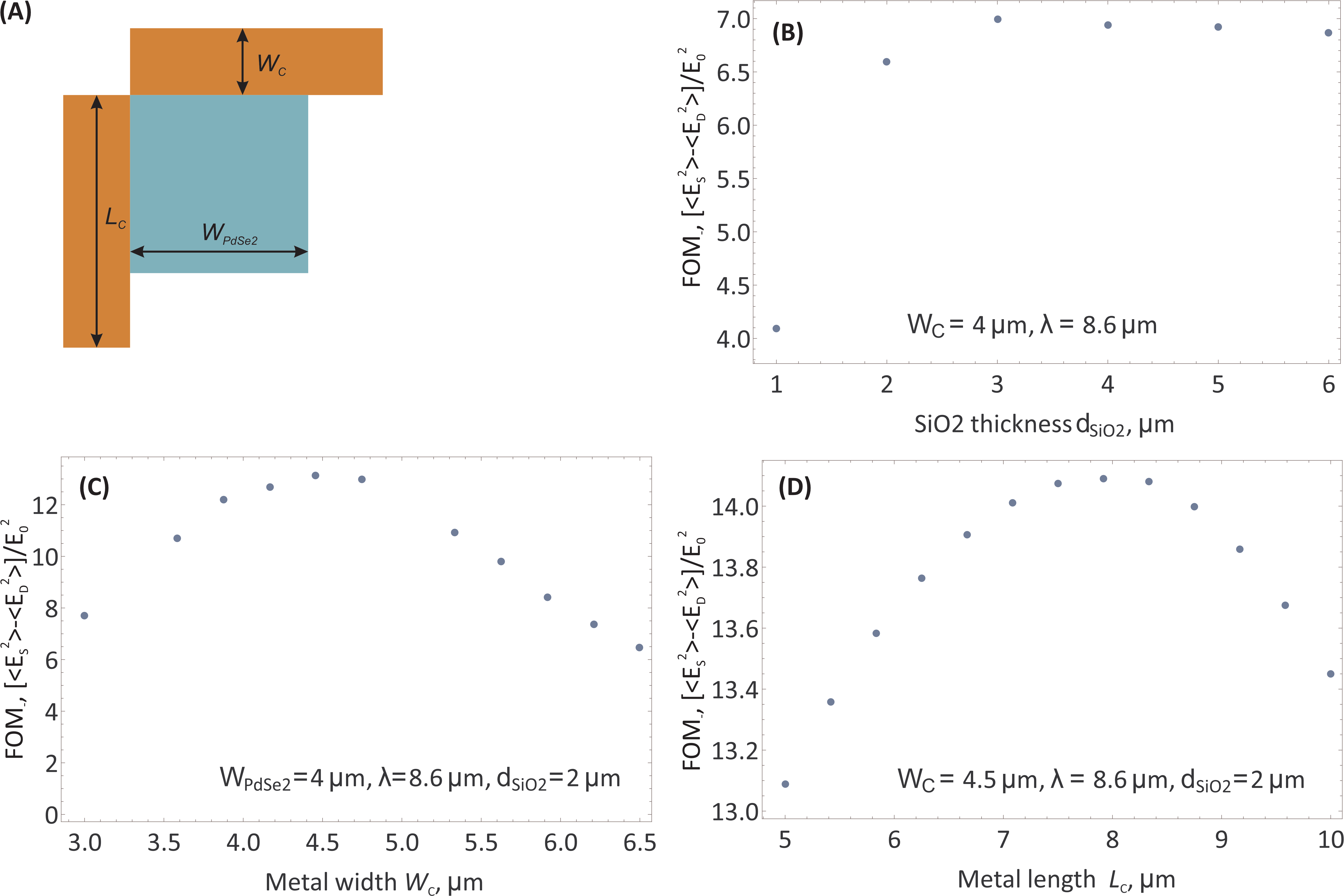
It appears that the most crucial parameter for optimization is the thickness of SiO2 substrate [Fig. S8 (b)]. If the oxide thickness is well below the radiation wavelength, FOM- takes very low values due to destructive interference of the incident wave and the wave reflected from high-index Si substrate. At m, the figure of merit almost saturates at its maximum value. No interference pattern is observed upon variation of oxide thickness due to large phonon absorption at our particular wavelength m.
Fixing the technologically achievable SiO2 thickness to 2 m, we vary the contact width in Fig. S8 (c). The maximum FOM is achieved at m. This width corresponds to the lowest dipole antenna-type resonance at metal width. Further optimization with respect to metal length [Fig. S8 (d)] raises the FOM- up to . The optimum is now achieved at m. Such length corresponds to antenna-type anti-resonance in the contact parallel to the polarization of the incident radiation.
To conclude, an optimized detector should reside on a thick oxide layer to avoid the interference-type suppression of the incident field. The width of metal contacts should be tuned approximately to , while their length – approximately to . This provides maximum field enhancement at the ’active’ Schottky contact and maximum field suppression at the ’passive’ one.