supp_mat
Spin-momentum locking and ultrafast spin-charge conversion in ultrathin epitaxial Bi1-xSbx topological insulator.
Abstract
The helicity of 3D topological insulator surface states has drawn significant attention in spintronics owing to spin-momentum locking where the carriers’ spin is oriented perpendicular to their momentum. This property can provide an efficient method to convert charge currents into spin currents, and vice-versa, through the Rashba-Edelstein effect. However, experimental signatures of these surface states to the spin-charge conversion are extremely difficult to disentangle from bulk state contributions. Here, we combine spin- and angle-resolved photo-emission spectroscopy, and time-resolved THz emission spectroscopy to categorically demonstrate that spin-charge conversion arises mainly from the surface state in Bi1-xSbx ultrathin films, down to few nanometers where confinement effects emerge. We correlate this large conversion efficiency, typically at the level of the bulk spin Hall effect from heavy metals, to the complex Fermi surface obtained from theoretical calculations of the inverse Rashba-Edelstein response. Both surface state robustness and sizeable conversion efficiency in epitaxial Bi1-xSbx thin films bring new perspectives for ultra-low power magnetic random-access memories and broadband THz generation.
Introduction
The discovery of metallic quantum states at the surface of 3D topological insulators (TIs) [1, 2, 3] has opened exciting new functionalities in spintronics owing to their topological protection and spin-momentum locking (SML) properties [4, 5]. Indeed, the combination of band inversion and time reversal symmetry (TRS) results in a peculiar spin texture in momentum space. Injecting a current in these states results therefore in an out of equilibrium spin density (also called spin-accumulation) along the transverse direction [4, 5, 6]. This is the Rashba-Edelstein effect (REE) [7] which can be used to exert a spin-orbit torque (SOT) onto the magnetization of an adjacent ferromagnet (FM) [8]. The reciprocal phenomenon, by which a spin density produces an in-plane transverse charge current, is called the Inverse Rashba-Edelstein effect (IREE) [9, 6].
Importantly, the resulting spin-charge conversion (SCC) efficiencies in topological surface states (TSS) combining strong spin-orbit coupling (SOC) and SML is expected to be at least one order of magnitude larger compared to the spin Hall effect (SHE) of 5d heavy metals [10, 11, 12]. SCC has been demonstrated in a range of Bi-based TI coumpounds, including bismuth selenide Bi2Se3, bismuth telluride Bi2Te3, Bi2(Se,Te)3 [13] or Bi1-xSbx (BiSb) [14]. To benefit fully from IREE, the charge currents should be confined in the surface states and any current flowing through the bulk states should be avoided. The prerequisites are hence i) a sizeable bandgap typically larger than 0.2 to 0.3 eV, and ii) a perfect control of the Fermi level position, usually achieved by stoichiometry and/or strain engineering. In this respect, Bi1-xSbx alloys, although displaying clear topological surface states [15, 16, 17], have been mostly neglected for spintronic applications as a result of their modest bulk bandgap (about 40 meV for ) and relatively complex band structure. However, quantization effects in ultrathin films have shown to lead to much larger gap [18, 19] while retaining their band inversion near the point in the composition range [20], unlike pure Bi [21, 22, 23]. BiSb therefore has considerable potential as candidate for spintronics applications as well as for recently engineered efficient spintronic THz emitters [24, 25, 26, 27, 28, 29, 30, 31].
In this letter, we report on our detailed investigation of the surface state SML properties of ultrathin (1 1 1)-oriented Bi1-xSbx epitaxial films. They exhibit a topological phase as recently confirmed by our angular-resolved photo-emission spectroscopy (ARPES) measurements [18]. Here, we focus on spin-resolved ARPES (SARPES) performed on ultrathin BiSb films and extract the in-plane spin texture for the different electron and hole pockets characterizing the complex BiSb Fermi surface. Moreover, the SCC mediated by the BiSb surface states is probed at the sub-picosecond timescale using an adjacent metallic Co layer acting as a spin injector. Unprecedentedly large SCC is measured with efficiencies beyond the level of carefully optimized Co/Pt systems. Our results also indicate that surface state related IREE is the mechanism responsible for SCC mechanism. Tight-binding (TB) calculation and linear response theory account for our findings.
I Spin-resolved ARPES
SARPES is the method of choice to probe the spin-textured Fermi contour of TI surfaces. Ultrathin epitaxial Bi1-xSbx films with , 0.1, 0.15, 0.21, 0.3, 0.4 and thicknesses down to 2.5 nm were grown by molecular beam epitaxy (MBE) on clean reconstructed Si(1 1 1) surfaces. They all exhibit a non-trivial topological phase. Details of the growth [32] are quickly recalled in the Methods section where scanning transmission electron microscopy (STEM) and energy-dispersive X-ray spectroscopy (EDX) characterizations are also discussed. We focus first on the 5 nm thick Bi0.85Sb0.15 sample. Fig. 1a shows its experimental Fermi surface within the 2D surface Brillouin zone, as measured by ARPES. It is composed of three pockets labelled (the hexagonal electron pocket surrounding ), and two elongated hole and electron pockets along each of the six equivalent directions (one has been chosen as the axis). Fig. 1b displays the energy dispersion along the direction. The signature of two surface and states [17, 18] are visible in the bandgap. The valence band state energy dispersion is also visible, from a series of confined states with energy splitting increasing with reducing thickness [18]. The corresponding experimental SARPES polarization map for the spin-polarization component is given in Fig. 1c. For this experiment, the incident photon energy is eV (5 meV resolution).
Owing to the electron analyzer movable entrance optics, the and spin polarizations were measured on a large part of the surface first Brillouin zone (see Methods). On Fig. 1e, the spin polarization is represented as a vector field. For clarity, the measured polarization is only displayed for positions where the DOS is the largest. The norm is roughly proportional to the spin-resolved DOS (s-DOS). The vector field is superimposed over a color map yielding the sum of all the signals measured by the spin detector, which is proportional to the DOS at the Fermi level. For a clearer representation, the vector fields were averaged over Å-2 areas, corresponding to twenty data points. The experimental data reveals the helical spin texture of the inner Fermi contour, the opposite spin polarization of the hole pocket, and finally, the same spin chirality for weaker pocket. We recover from experiments the symmetry property imposing the orthogonality between the spin direction and the vertical symmetry planes containing the lines. Such property remains partly true concerning the in-plane spin components for the directions even if the corresponding vertical planes do not represent perfect symmetry operators. The lack of symmetry for leads to the warping term responsible for the appearance of a component [2], not presently discussed.
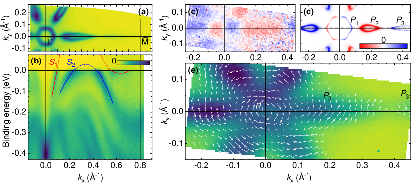
We now compare the and surface state spin-texture with a TB model. Calculations are implemented by considering relaxed bulk lattice parameters following the Vegard’s law (refer to Ref. [18] and Methods). The electronic band structure and energy band dispersion along are plotted in the Suppl. Mat. LABEL:S_HRARPES showing a good agreement with ARPES data. The s-DOS at the Fermi surface, originating from and , and projected on the top surface (first BL, ) is displayed in Fig. 1d. The color code represents the -DOS projected onto the first BL. Around , positive (negative) values are observed for positive (negative) . The sign of this Rashba field is opposite around the point (close to 0.8 Å-1). Two electron (, ) and one hole () pockets emerge, in very good agreement again with (S)ARPES data. By introducing the Rashba surface potential imposed by the surface symmetry breaking, we are able to reproduce the spin-resolved map over the projected 2D-Brillouin onto the first BiSb BL (see Methods).
II Ultrafast spin-charge conversion in Bi1-xSbx/Co probed by THz-TDS emission spectroscopy.
With the clear demonstration of the spin resolved surface states, we now discuss the dynamical spin-charge conversion in Bi1-xSbx capped by a thin Co layer as a spin-injector. THz emission spectroscopy in the time domain (THz-TDS) has recently emerged as a powerful spectroscopic technique to investigate ultrafast SCC in materials with strong SOC [24] and, in particular, in TI/FM structures [26, 25, 27, 31]. The thin FM layer is excited by a femtosecond laser pump leading to ultrafast demagnetization. This generates both spin density and spin-current diffusing toward the BiSb/Co interface owing to the two spin populations and mobilities introduced by the sp-band spin-splitting in Co [33]. The spin is afterwards converted into a transverse charge flow on sub-picosecond timescales leading to a THz transient emission that is directly probed in the time-domain (see Refs. [24, 33] and Methods). Two SCC mechanisms can contribute: the IREE from the surface states and the ISHE from the bulk. The THz electric field can be expressed as:
| (1) |
where is the Co layer magnetization vector, is the spin-accumulation vector relaxing on and and is the frequency. can be controlled by an external in-plane magnetic field at an angle from the axis. In the above equation, is the spin Hall angle scaling the bulk ISHE-mediated SCC, whereas is the Rashba-Edelstein length scaling the IREE from the surface states (refer to Methods and Suppl. Mat. LABEL:S_lin_resp_th).
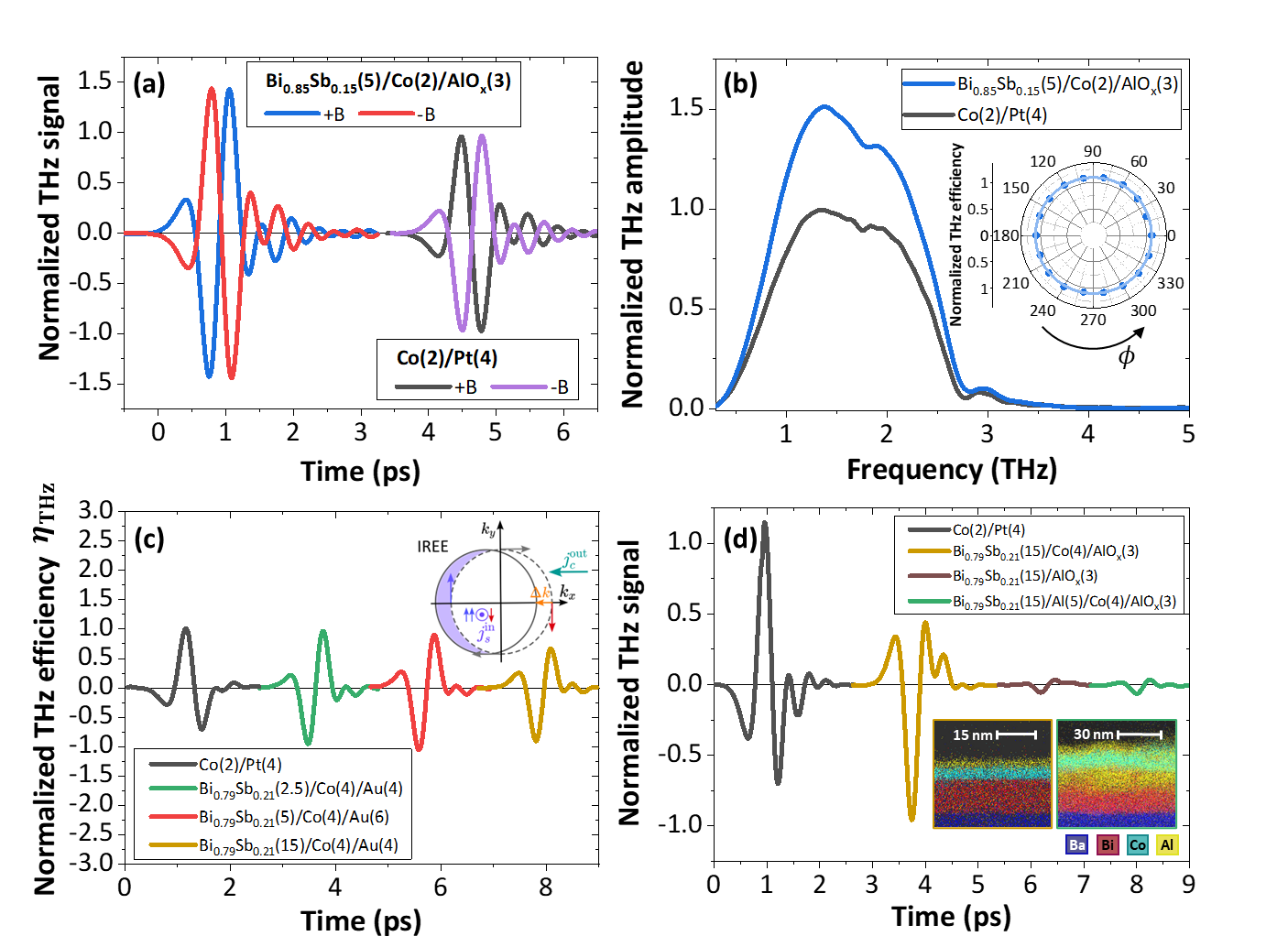
On Fig. 2a, we report the THz signal acquired in reflection geometry from Bi0.85Sb0.15(5)/Co(2) sample (numbers in parenthesis are thicknesses in nm) at room temperature with a saturating in-plane magnetic field mT insuring that the magnetization follows the external field within much less than a degree. It is compared to the emission from our optimized Co(2)/Pt(4) metallic ISHE-type sample. In both cases, we observe a short picosecond THz pulse with some minor oscillations within a 3 ps wide envelope. The THz signal phase changes sign when reversing the magnetic field, in full agreement with SCC-mediated THz emission (Suppl. Mat. LABEL:S_dipolar). We note several differences: first, the amplitude from the BiSb/Co layer is 1.5 times larger than the Co/Pt revealing the large SCC efficiency in BiSb. For the same magnetic field orientation, the BiSb/Co THz signal phase is opposite to the one found in the Co/Pt sample (Fig. 2a): this sign inversion is related to the inverted layer stacking of the FM and non magnetic layer, giving an opposite phase and indicating that Pt and BiSb share the same conversion sign.
We also report in Fig. 2b the THz spectra (Fourier transform) obtained from Co(2)/Pt(4) and Bi1-xSbx(5)/Co(2), demonstrating a relative power enhancement by a factor for the Bi1-xSbx/Co sample (field enhancement by a factor 1.5). The THz amplitude of Bi1-xSbx/Co is also shown to scale linearly with the pump fluence (Suppl. Mat. LABEL:S_fluence), measured up to a few tens of µJ.cm-2. The azimuthal angular dependence of the THz emission obtained by rotating the sample in the plane by an angle , while keeping fixed the magnetic field, is shown in the inset of Fig. 2b. The emission is almost isotropic revealing a pure SCC phenomenon with no evidence of non-linear optical effects such as shift or surge current contributions (e.g. photon drag, photogalvanic effects, etc.). This is in contrast with the recent report given by Park et al. [30] where additional but small non-magnetic contributions were observed. At normal incidence of the optical pump pulse, a pure isotropic THz response vs. is expected from the linear response theory for both ISHE and IREE scenario (Suppl. Mat. LABEL:S_lin_resp_th) as discussed here. The role of the capping layer (metallic Au or oxidized Al, AlOx) has been carefully excluded by control experiments (Suppl. Mat. LABEL:S_capping). Two additional control samples were grown: i) a Bi0.79Sb0.21(15 nm) sample free of ferromagnetic Co and only capped with naturally oxidized AlOx(3 nm) almost emitting no THz radiation (Fig. 2d) and ii) a sample with a 5 nm thick Al metallic spacer inserted between BiSb and Co. The Al insertion strongly reduces the THz emission. It may be explained either by a larger near-infrared (NIR) and THz absorption in Al, or by interfacial spin-loss or weakening of the surface SCC induced by the strong degradation of the interface quality. Indeed, TEM pictures displayed in the inset of Fig. 2d reveal a strong intermixing of the Al interlayer that may induce a loss of an efficient spin-injection and/or the alteration of the surface states (more details in Suppl. Mat. LABEL:S_interface).
To get a better insight into the SCC mechanism, the thickness dependence of the THz efficiency, , is displayed in Fig. 2c for the Bi0.79Sb0.21 series (2.5, 5 and 15 nm thick layers). represents the spin-injection and conversion efficiencies and is obtained by withdrawing the NIR and THz absorptions in the heterostructure following the procedure proposed in Refs. [34, 35, 36] (Suppl. Mat. LABEL:S_efficiency). Strikingly, for BiSb remains constant for the whole thickness series where the BiSb bandgap widens dramatically by several hundreds of meV as the thickness is reduced, as calculated previously [18]. Moreover, in agreement with our ARPES results [18], this demonstrates the absence of coupling between the top and bottom surface states [37] down to 2.5 nm, unlike previously argued in the case of sputtered BiSb materials [28]. The characteristic evanescence length is indeed ultrashort, typically 2 BL (0.8 nm) near as confirmed by density functional theory [38] for pure Bi and confirmed by our TB calculation (Suppl. Mat. LABEL:S_lin_resp_th). Such behavior is therefore more in favor of an interfacial origin of the SCC and thus strongly hints towards IREE from the surface states rather than ISHE from bulk.
Furthermore, when considering the possible contribution of bulk ISHE, BiSb thickness has to be compared with its spin diffusion length. It has been evaluated in bulk BiSb at 8 nm by Sharma et al. [28], which is much larger than 2.5 nm. If bulk states were to contribute via ISHE, the spin current would therefore flow across the whole layer depth, and upper and lower interfaces would contribute similarly to the SCC but with an opposite sign. The net charge current would drop to zero, as [39] for small TI thicknesses when considering the multiple spin current reflections at the TI interfaces [36]. This is in contrast with the thickness-independent SCC observed here, in the ultrathin limit. We thus anticipate that the bulk states are hardly involved, and that the surface states at the FM/TI interface are mainly responsible for a net charge current through IREE. This conclusion is also supported by i) the large increase of the surface state DOS of BiSb at the interface compared to the DOS bulk states as the BiSb thickness increases (see Suppl. Mat. LABEL:S_lin_resp_th) and by ii) the assumption of the preservation of BiSb surface states in exchange contact with Co as it seems to be the case.
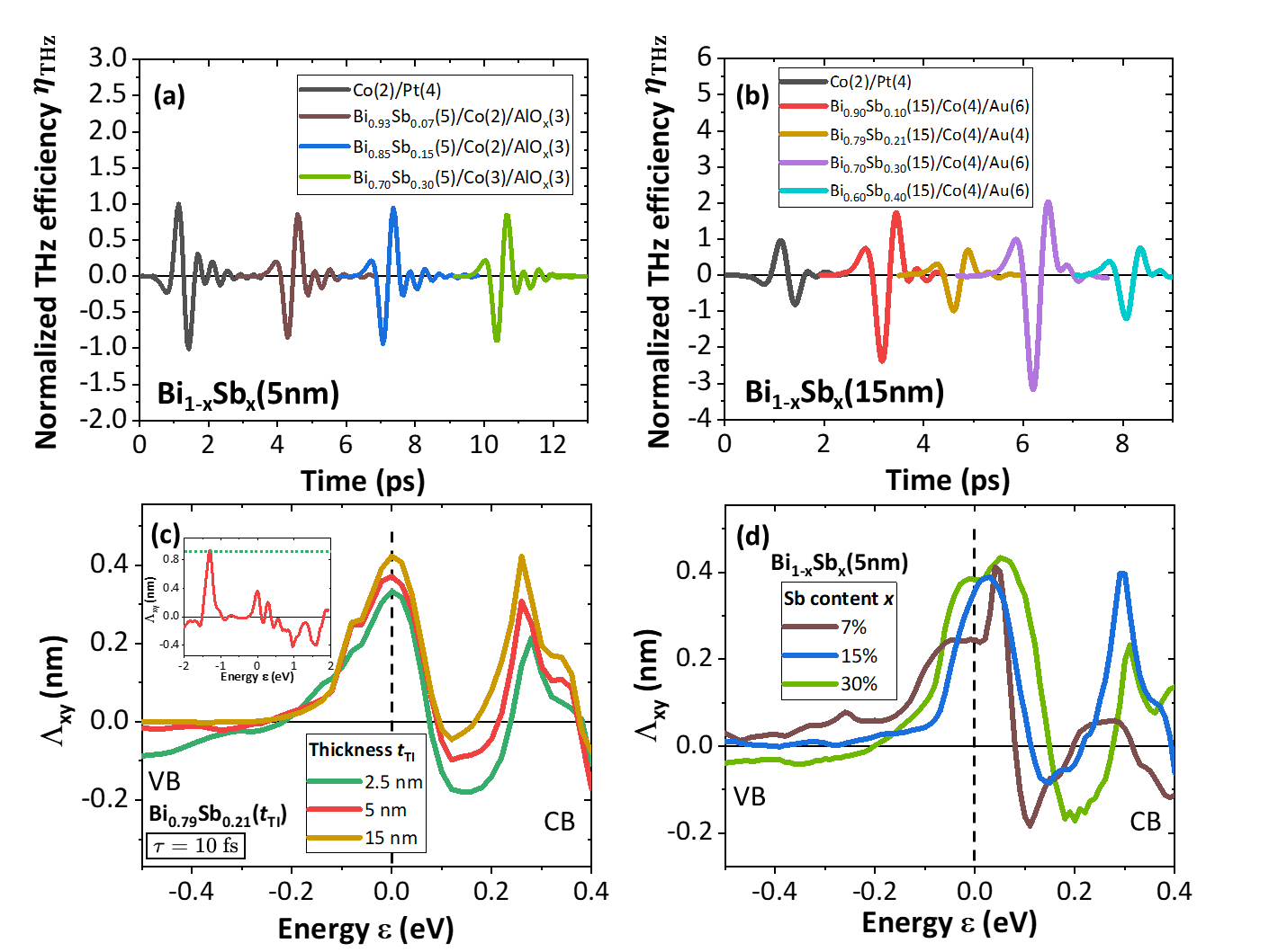
We now focus on the THz efficiency vs. the Sb content , plotted for Bi1-xSbx(5)/Co(2)/AlOx(3) in Fig. 3a and for Bi1-xSbx(15)/Co(4)/Au in Fig. 3b (Suppl. Mat. LABEL:S_concentration). In each series, a large is measured, comparable to that of Co/Pt with a maximum for for the 15 nm series, i.e. at the limit of the topological phase diagram [20]. Importantly, remains similar for all the samples for the nm series (Fig. 3a), highlighting again the prominent role of the surface states in the SCC. It also emphasizes the robustness of the IREE over a wide range of Sb content. The persistence of a large signal outside the bulk topological window ( for 15 nm thickness, in Fig. 3b) indicates that bulk states may start to contribute by shunting a part of the spin current.
III SCC and IREE tensor from Linear Response theory
We now compare the enhanced THz emission observed on ultrathin BiSb films to that obtained from the linear response theory described by the IREE response, namely matching with the so-called inverse Edelstein length (see Suppl. Mat. LABEL:S_lin_resp_th and Methods). We consider an extended formalism to the one recently developed to address the direct REE response as given in Refs. [40, 41, 42]. We evaluate here the intraband response to an ongoing spin-current relaxing onto the Fermi surface generating, via an out-of-equilibrium spin-density, a charge current according to: with where is the direction of the spin injected with a flow along whereas is the direction of the in-plane charge current. In the above expression, is the band index, the corresponding band velocity along and is the typical (spin) relaxation time assumed to be constant onto the Fermi surface. is the occupation number for the band and wavevector whereas represents the local DOS in the k space.
Calculations are performed on bare BiSb bilayers (BLs) free of any Co overlayer as investigated by SARPES. We show, on Fig. 3c, the energy dependence of obtained for Bi0.79Sb0.21 of different film thicknesses: 2.5, 5 and 15 nm (see Methods). The Fermi level position corresponds to . One observes that is largely enhanced in the bandgap region in the (-0.2 - 0.2) eV window where the surface state and TSS are located, however without being able to differentiate their individual contributions (see Fig. LABEL:figS_IREEthick for the corresponding DOS in the Suppl. Mat. LABEL:S_lin_resp_th). remains constant vs. BiSb film thickness in this window range, as experimentally observed in THz data of Fig. 2c. Last, is maximum at the Fermi level, where it reaches values in the range of the equivalent SCC efficiency of Pt, product of the spin-Hall angle by the spin-diffusion length as nm for the same spin or momentum relaxation time ( fs). Increasing the spin-relaxation onto the surface states to 30 fs would yield nm. is displayed in Fig. 3c as a function of the Sb content for the 5 nm series. Although one observes a slight increase of the SCC response from =0.1 to 0.3 in the gap window (still in line with the presence of the surface states, and possibly indicating a volume contribution), one may conclude that the SCC remains roughly constant at the vicinity of the Fermi energy (). This is observed experimentally from THz-TDS measurements, and thus suggests an interfacial IREE nature of the SCC, at least for the thinner films. One cannot totally rule out a certain ISHE contribution arising from the bulk propagating bands associated to a very short spin-diffusion length. Nonetheless, the strong impedance mismatch and subsequent spin-backflow at Co/BiSb interface would be strongly in disfavor of such scenario.
Conclusions
Although less investigated compared to other Bi-based families because of its modest bandgap, BiSb ultrathin films still exhibit very robust surface states, as revealed by our spin-resolved ARPES measurements. This is in part related to the confinement effects without being detrimental to the surface states. In particular, the presence of a topological surface state in a wide Sb-composition and thickness ranges is clearly observed, displaying helical spin texture at the Fermi surface with a specific opposite chirality between the electron pocket near the point and the six hole pockets away from . Via ultrafast THz emission spectroscopy, we demonstrate that the complex spin-texture gives rise to a very efficient spin-charge conversion, resulting from the spin-injection from a Co overlayer excited by an ultrashort laser pulse, mainly occurring via inverse Rashba-Edelstein effect (IREE) owing to the strong localization of the surface states. Our results address the role of spin-textured hybridized Rashba-like surface states offering unprecedented SCC efficiency despite the breaking of the TRS symmetry due to the local exchange interactions imposed by the magnetic contact. These results hold promise for efficient and integrated structures based on BiSb. Future investigations will concern the dynamics of the spin relaxation onto the BiSb surface states excited by ultrashort pulses.
Acknowledgments
We thank T. Kampfrath and G. Bierhance (Freie Universität Berlin) for very fruitful discussions. This work was supported by a grant overseen by the French National Research Agency (ANR) as part of the “Generic Project Call - 2021” Programme (ANR-21-CE24-0011 TRAPIST), public grant overseen by the French National Research Agency (ANR) as part of the “Investissements d’Avenir” program (Labex NanoSaclay, reference: ANR-10-LABX-0035 SPICY) and the program ESR/EquipEx+ (Grant No. ANR-21-ESRE-0025). We acknowledge financial support from the Horizon 2020 Framework Programme of the European Commission under FET-Open Grant No. 863155 (s-Nebula) and Grant No. 64735 (Extreme-IR).
Author contributions
J.-M.G., H.J., P.LF., S.D. and A.L. conceived and designed the experiment. J.-M.G. supervised the project. L.B., D.S., Ma.Mo., A.L., N.R., F.B., P.LF. and J.-M.G. grew the samples and performed ARPES and SARPES experiments at Synchrotron Soleil. G.P, L.B. and A.L. performed TEM cross-section and SR-TEM microscopy. E.R, S.D., Ma.Mi., Ju.M., J.T. performed THz-TDS experiments at room temperature. H.J. performed TB calculations. E.R., P.LF., S.D., A.L., R.L., N. R., H.J, J.-M.G. analysed the data. E.R., P.LF., S.D., A.L., N. R., R.L., H.J., J.-M.G. wrote the paper.
Methods
MBE growth of Bi1-xSbx. The Bi1-xSbx samples were grown by Molecular Beam Epitaxy (MBE). A Si(111) substrate was annealed in ultra-high vacuum (UHV) at 1370 K in order to obtain a 77 surface reconstruction, observed by reflection high energy electron diffraction (RHEED). The Bi1-xSbx alloy is grown by co-deposition from two Knudsen cells. Each cell flux is calibrated prior to the deposition using a quartz microbalance and the relative deposition rates are directly used to estimate the Sb-concentration . RHEED measurements are performed throughout the deposition. Up to 5 nm, we observe a 2D-growth; for thicker films, we stop the evaporation at 7 nm for a 10 min intermediate annealing at 500 K before completing the film growth up to the targeted thickness. This procedure is further described in Ref. [18]. BiSb films with thicknesses from 2.5 to 15 nm and with various compositions (0.03<<0.3) were grown using this method and their crystallographic quality was demonstrated by RHEED, X-ray-diffraction or Scanning Transmission Electron Microscopy (STEM) [18].
All our samples were grown in the MBE chamber of the CASSIOPEE beamline installed on the SOLEIL synchrotron. After their elaboration, they can be transferred in UHV to an ARPES (Angle-Resolved PhotoEmission Spectroscopy) or a SARPES (Spin-Resolved ARPES) experiments where we can characterize their electronic structure. After photoemission measurements, some of the sample were transferred again into the MBE chamber for Co electron beam deposition. These bilayer systems were used for SCC measurements using THz emission spectroscopy.
SEM - FIB milling and EDX. Lamellae for STEM observation were prepared from the sample using Focused Ion Beam (FIB) ion milling and thinning. Prior to FIB ion milling, the sample surface was coated with 50 nm of carbon to protect the surface from the platinum mask deposited used for the ion milling process. Ion milling and thinning were carried out in a FEI SCIOS dual-beam FIB-SEM. Initial etching was performed at 30 keV, and final polishing was performed at 5 keV. The lamellae were prepared following the two different zone axis ( and ) of the BaF2 substrate. All samples were observed in an aberration-corrected FEI TITAN 200 TEM-STEM operating at 200 keV. The convergence half-angle of the probe was 17.6 mrad and the detection inner and outer half-angles for HAADF-STEM were 69 mrad and 200 mrad, respectively. All micrographs where 2048 by 2048 pixels. The dwell time was 8 µs and the total acquisition time 41 s. EDX measurements were performed in the Titan microscope featuring the Chemistem system, that uses a Bruker windowless Super-X four-quadrant detector and has a collection angle of 0.8 sr.
(Spin-)Angular-resolved photoemission spectroscopy. The photoemission experiments were performed on the CASSIOPEE beamline installed on the SOLEIL storage ring (Saint-Aubin, France). The beamline hosts two endstations. A high-resolution ARPES endstation, which was used in this work for the measurement of the Fermi surface and of the band dispersion, using 20 eV incident photons with a linear horizontal polarization. It is equipped with a Scienta R4000 electron analyzer. The photon spot size on the sample is of the order of 5050 µm2 and the overall kinetic energy resolution (taking into account both the photon energy and the electron kinetic energy resolutions) was of the order of 10 meV. The second endstation is a spin-resolved ARPES experiment, where the beam size is around 300300 µm2. It is equipped with a MBS A1-analyzer with a 2D detector for ARPES measurements. Close to this 2D detector, a 11 mm2 hole collects photoelectron with well-defined kinetic energy and momentum. They are sent into a spin manipulator able to orient any spin component along the magnetization axis of a FERRUM VLEED spin-detector, made of a Fe(100)-p(11)O surface [43, 44] deposited on a W-substrate.
The spin polarization along the selected direction is proportional to the difference of the two signals collected for opposite magnetizations of the Fe-oxide target. To reduce as much as possible the measurement asymmetries stemming from the instrument (i.e., not due to the spin polarization), four measurements per polarization direction are acquired, reversing both the ferrum magnetization direction, and the electron spin direction. This four measurements are combined into a geometrical average. The polarization is then determined by .
The 11 mm2 hole introduces an integration on both the kinetic energy and the wave vector. For the kinetic energy, it corresponds to 0.23% of the used pass energy (10 eV in our case), so around 23 meV. Convoluted with the energy resolution of the analyzer (10 meV for this pass energy and an entrance slit of 400 µm), it gives an overall kinetic energy resolution of 25 meV. For the wave vector, the 1 mm aperture corresponds to an integration on 4% of the total (30∘) angular range, which gives 1.2∘. At 20 eV photon energy, for electrons at the Fermi level, this gives a -resolution of around 0.048 Å-1. This explains the relatively broad features of the SARPES in Fig. 1c,e compared to Fig. 1a.
The analyzer optics is movable and can collect electrons in a large 2D (30) angular range. To map the spin texture at the Fermi level, the analyzer is set to the appropriate kinetic energy while the optics is moved by 0.2∘ step along two X and Y perpendicular directions. The two in-plane spin components are measured at each step.
THz emission spectroscopy. Ultrafast near-infrared (NIR) pulses (100 fs) centered at =810 nm are derived from a Ti:Sapphire oscillator to photo-excite the spin carriers directly from the front surface (Co side). Average powers of up to 600 mW were used with a repetition rate of 80 MHz (the energy per pulse is around 3 nJ). The typical laser spot size on the sample was about 200 µm 200 µm. The optical pump is initially linearly polarized and irradiate the TI/FM heterostructure under normal incidence. The generated THz pulses were also collected from the front surface of the samples (i.e., reflection geometry) using a set of parabolic mirrors of 150 and 75 mm focal length to focus on the detection crystal. The samples were placed on a mount with a small magnetic field (around 100 mT) in the plane of the thin films. Both the sample orientation (angle ) and the in-plane magnetic field (angle ) can be independently rotated in the sample plane. Standard electro-optic sampling was used to detect the electric field of the THz pulses, using a 500 µm-thick ZnTe crystal. A chopper was placed at the focal point between the second and third parabolic mirror to modulate the THz beam at 6 kHz for heterodyne lock-in detection. A mechanical delay line was used to sample the THz ultrafast pulse as a function of time. The THz propagation path was enclosed in a dry-atmosphere purged chamber (typically <2% humidity) to reduce water absorption of the THz radiation.
Tight-binding calculations of Bi1-xSbx multilayers. We have developed a tight binding (TB) model in order to describe the Bi1-xSbx electronic band structure as well as their surface topological properties [45]. This approach is indeed well suited for TI and gives a fair description of the surface state spin texture in close agreement with the one derived from Density Functional Theory (DFT) developed for pure Bi surfaces [46, 21, 22]. The rhombohedral A7 structure is described by two atoms per unit cell, forming then a bilayer (BL) of thickness of about 0.4 nm. Bi1-xSbx slabs are obtained by stacking the BL along the (1 1 1) direction ( axis) with two different plane-to-plane distances. We constructed our Hamiltonian on the basis of the work of Ref. [45] using the generalization of the sp3 TB-model Hamiltonian proposed for bulk Bi and Sb crystals [47], adapted to Bi1-xSbx alloys [15] and complemented by the introduction of additional surface potential terms when dealing with thin layers (treatment in slabs) [48, 49, 45]. In particular, the hopping parameters for the BiSb alloys are obtained by using the virtual crystal approximation (VCA) according to [15]:
| (2) |
where is the antimony content and and are the respective hopping parameters of Sb and Bi taken from Ref. [47]. One notes the spin index on each atom where stands for the directional index. The hopping terms among the atomic orbitals are decomposed into inter- and intra-BL hopping terms. The inter-BL off-diagonal hopping term between atoms (plane) 1 and atoms (plane) 2 consists of the nearest-neighbor coupling in the bulk BiSb Hamiltonian, whereas the intra-BL hopping term consists of two parts which represents respectively the third and second nearest neighbor contributions. We considered the overall TB Hamiltonian according to:
| (3) |
where represents the hopping Hamiltonian (, are the atomic positions, , are the orbitals), the SOC term and the Rashba surface potential induced by the deformation of the surface orbitals due to the local electric field. Indeed, due to the symmetry breaking at the surface, a Rashba SOC term must be taken into account in the Hamiltonian at the two surface planes. We model such effect for the basis by using the approach of Ast and Gierz [49] for considering two additional surface hopping terms and acting respectively between the and (or ) surface orbitals. We thus add the Hamiltonian term of the form:
| (8) |
where the + (-) sign corresponds to the uppermost (lowermost) atomic plane and is the angle between the direction joining the two atoms considered and the -direction. We then restrained ourselves to the in-plane surface hopping as for a pure 2D system. The best agreement with ARPES results is found by adding, as proposed in Ref. [49], additional on-site coupling eV, and surface hopping terms =0.3 eV and =-0.6 eV for =0.15 slightly departing from the values given for pure Bi, i.e. =0.45 eV and =-0.27 eV [45], with opposite sign for the top and bottom surfaces due to the opposite direction of the potential gradient. We emphasize that this surface terms are required to correctly reproduce the surface state dispersion as observed by ARPES experiments. The size of the Hamiltonian to diagonalize is where is the number of bilayers (BLs). Once the Green function of the multilayer system is defined as:
| (9) |
the partial density of state (DOS) vs. the energy equals whereas the spin density of states (spin-DOS) with spin along the direction is . is the typical energy broadening ( 10 meV) and the trace () is applied over the considered orbitals on a given BL index (). The energy zero (=0) refers to the Fermi level position.
The modelling of IREE were performed by TB method. We have summed the contributions from the different Fermi surface pockets within the 2D-BZ after i) having introduced the Rashba potentials at the BiSb surfaces, required to match both the TSS electronic dispersion and SML measured in (S)ARPES experiments [18]; and after ii) having considered a same (spin) relaxation time of fs involved in the intraband transitions. The inverse Edelstein length has been then evaluated on the whole Fermi surface according to the following expression (see Suppl. Mat. LABEL:S_lin_resp_th).
The typical value of fs corresponds to an energy broadening meV) and a Fermi velocity of about m.s-1 like extracted from ARPES data. The trace on is performed by summing the BL contributions from the top surface down to the middle of the BL, typically matching the typical finite TSS evanescence or extension length.
References
- [1] M. Z. Hasan and C. L. Kane, “Colloquium : topological insulators,” Reviews of Modern Physics, vol. 82, pp. 3045–3067, Nov. 2010.
- [2] Y. Ando, “Topological Insulator Materials,” Journal of the Physical Society of Japan, vol. 82, p. 102001, Oct. 2013.
- [3] X.-L. Qi and S.-C. Zhang, “Topological insulators and superconductors,” Reviews of Modern Physics, vol. 83, pp. 1057–1110, Oct. 2011.
- [4] Y. Shiomi, K. Nomura, Y. Kajiwara, K. Eto, M. Novak, K. Segawa, Y. Ando, and E. Saitoh, “Spin-Electricity Conversion Induced by Spin Injection into Topological Insulators,” Physical Review Letters, vol. 113, p. 196601, Nov. 2014.
- [5] Y. Ando and M. Shiraishi, “Spin to Charge Interconversion Phenomena in the Interface and Surface States,” Journal of the Physical Society of Japan, vol. 86, p. 011001, Jan. 2017.
- [6] W. Han, Y. Otani, and S. Maekawa, “Quantum materials for spin and charge conversion,” npj Quantum Materials, vol. 3, p. 27, Dec. 2018.
- [7] V. Edelstein, “Spin polarization of conduction electrons induced by electric current in two-dimensional asymmetric electron systems,” Solid State Communications, vol. 73, pp. 233–235, Jan. 1990.
- [8] A. R. Mellnik, J. S. Lee, A. Richardella, J. L. Grab, P. J. Mintun, M. H. Fischer, A. Vaezi, A. Manchon, E.-A. Kim, N. Samarth, and D. C. Ralph, “Spin-transfer torque generated by a topological insulator,” Nature, vol. 511, pp. 449–451, Jul 2014.
- [9] S. Zhang and A. Fert, “Conversion between spin and charge currents with topological insulators,” Physical Review B, vol. 94, p. 184423, Nov. 2016.
- [10] I. M. Miron, K. Garello, G. Gaudin, P.-J. Zermatten, M. V. Costache, S. Auffret, S. Bandiera, B. Rodmacq, A. Schuhl, and P. Gambardella, “Perpendicular switching of a single ferromagnetic layer induced by in-plane current injection,” Nature, vol. 476, pp. 189–193, Aug. 2011.
- [11] L. Liu, O. J. Lee, T. J. Gudmundsen, D. C. Ralph, and R. A. Buhrman, “Current-Induced Switching of Perpendicularly Magnetized Magnetic Layers Using Spin Torque from the Spin Hall Effect,” Physical Review Letters, vol. 109, p. 096602, Aug. 2012.
- [12] L. Liu, C.-F. Pai, Y. Li, H. W. Tseng, D. C. Ralph, and R. A. Buhrman, “Spin-Torque Switching with the Giant Spin Hall Effect of Tantalum,” Science, vol. 336, pp. 555–558, May 2012.
- [13] K. Kondou, R. Yoshimi, A. Tsukazaki, Y. Fukuma, J. Matsuno, K. S. Takahashi, M. Kawasaki, Y. Tokura, and Y. Otani, “Fermi-level-dependent charge-to-spin current conversion by Dirac surface states of topological insulators,” Nature Physics, vol. 12, pp. 1027–1031, Nov 2016.
- [14] N. H. D. Khang, Y. Ueda, and P. N. Hai, “A conductive topological insulator with large spin Hall effect for ultralow power spin–orbit torque switching,” Nature Materials, vol. 17, pp. 808–813, Sept. 2018.
- [15] J. C. Y. Teo, L. Fu, and C. L. Kane, “Surface states and topological invariants in three-dimensional topological insulators: Application to ,” Phys. Rev. B, vol. 78, p. 045426, Jul 2008.
- [16] D. Hsieh, D. Qian, L. Wray, Y. Xia, Y. S. Hor, R. J. Cava, and M. Z. Hasan, “A topological Dirac insulator in a quantum spin Hall phase,” Nature, vol. 452, pp. 970–974, Apr. 2008.
- [17] H. M. Benia, C. Straßer, K. Kern, and C. R. Ast, “Surface band structure of Bi1-xSbx(111),” Physical Review B, vol. 91, p. 161406, Apr. 2015.
- [18] L. Baringthon, T. H. Dang, H. Jaffrès, N. Reyren, J.-M. George, M. Morassi, G. Patriarche, A. Lemaitre, F. Bertran, and P. Le Fèvre, “Topological surface states in ultrathin Bi1-xSbx layers,” Physical Review Materials, vol. 6, p. 074204, July 2022.
- [19] S. Ito, M. Arita, J. Haruyama, B. Feng, W.-C. Chen, H. Namatame, M. Taniguchi, C.-M. Cheng, G. Bian, S.-J. Tang, T.-C. Chiang, O. Sugino, F. Komori, and I. Matsuda, “Surface-state Coulomb repulsion accelerates a metal-insulator transition in topological semimetal nanofilms,” Science Advances, vol. 6, no. 12, p. eaaz5015, 2020.
- [20] B. Lenoir, H. Scherrer, and T. Caillat, “An overview of recent developments for BiSb Alloys,” in Semiconductors and Semimetals, vol. 69, pp. 101–137, Elsevier, 2001.
- [21] T. Hirahara, T. Nagao, I. Matsuda, G. Bihlmayer, E. V. Chulkov, Y. M. Koroteev, P. M. Echenique, M. Saito, and S. Hasegawa, “Role of Spin-Orbit Coupling and Hybridization Effects in the Electronic Structure of Ultrathin Bi Films,” Phys. Rev. Lett., vol. 97, p. 146803, Oct 2006.
- [22] Y. M. Koroteev, G. Bihlmayer, E. V. Chulkov, and S. Blügel, “First-principles investigation of structural and electronic properties of ultrathin Bi films,” Phys. Rev. B, vol. 77, p. 045428, Jan 2008.
- [23] I. Aguilera, H.-J. Kim, C. Friedrich, G. Bihlmayer, and S. Blügel, “ topology of bismuth,” Physical Review Materials, vol. 5, p. L091201, Sept. 2021.
- [24] T. Seifert, S. Jaiswal, U. Martens, J. Hannegan, L. Braun, P. Maldonado, F. Freimuth, A. Kronenberg, J. Henrizi, I. Radu, E. Beaurepaire, Y. Mokrousov, P. M. Oppeneer, M. Jourdan, G. Jakob, D. Turchinovich, L. M. Hayden, M. Wolf, M. Münzenberg, M. Kläui, and T. Kampfrath, “Efficient metallic spintronic emitters of ultrabroadband terahertz radiation,” Nature Photonics, vol. 10, pp. 483–488, Jul 2016.
- [25] X. Wang, L. Cheng, D. Zhu, Y. Wu, M. Chen, Y. Wang, D. Zhao, C. B. Boothroyd, Y. M. Lam, J.-X. Zhu, M. Battiato, J. C. W. Song, H. Yang, and E. E. M. Chia, “Ultrafast Spin-to-Charge Conversion at the Surface of Topological Insulator Thin Films,” Advanced Materials, vol. 30, no. 52, p. 1802356, 2018.
- [26] M. Tong, Y. Hu, Z. Wang, T. Zhou, X. Xie, X. Cheng, and T. Jiang, “Enhanced Terahertz Radiation by Efficient Spin-to-Charge Conversion in Rashba-Mediated Dirac Surface States,” Nano Letters, vol. 21, no. 1, pp. 60–67, 2021. PMID: 33331788.
- [27] X. Chen, H. Wang, C. Wang, C. Ouyang, G. Wei, T. Nie, W. Zhao, J. Miao, Y. Li, L. Wang, and X. Wu, “Efficient Generation and Arbitrary Manipulation of Chiral Terahertz Waves Emitted from Bi2Te3–Fe Heterostructures,” Advanced Photonics Research, vol. 2, no. 4, p. 2000099, 2021.
- [28] V. Sharma, W. Wu, P. Bajracharya, D. Q. To, A. Johnson, A. Janotti, G. W. Bryant, L. Gundlach, M. B. Jungfleisch, and R. C. Budhani, “Light and microwave driven spin pumping across FeGaB–BiSb interface,” Phys. Rev. Materials, vol. 5, p. 124410, Dec 2021.
- [29] H. Park, K. Jeong, I. Maeng, K. I. Sim, S. Pathak, J. Kim, S.-B. Hong, T. S. Jung, C. Kang, J. H. Kim, J. Hong, and M.-H. Cho, “Enhanced Spin-to-Charge Conversion Efficiency in Ultrathin Bi2Se3 Observed by Spintronic Terahertz Spectroscopy,” ACS Applied Materials & Interfaces, vol. 13, no. 19, pp. 23153–23160, 2021. PMID: 33945256.
- [30] H. Park, S. Rho, J. Kim, H. Kim, D. Kim, C. Kang, and M. Cho, “Topological Surface-Dominated Spintronic THz Emission in Topologically Nontrivial Bi1-xSbx Films,” Advanced Science, p. 2200948, May 2022.
- [31] E. Rongione, S. Fragkos, L. Baringthon, J. Hawecker, E. Xenogiannopoulou, P. Tsipas, C. Song, M. Mičica, J. Mangeney, J. Tignon, T. Boulier, N. Reyren, R. Lebrun, J.-M. George, P. Le Fèvre, S. Dhillon, A. Dimoulas, and H. Jaffrès, “Ultrafast Spin-Charge Conversion at SnBi2Te4/Co Topological Insulator Interfaces Probed by Terahertz Emission Spectroscopy,” Advanced Optical Materials, vol. 10, no. 7, p. 2102061, 2022.
- [32] L. Baringthon, Élaboration et caractérisation de phases topologiques de l’alliage Bi1-xSbx pour la conversion spin charge. PhD thesis, Université Paris-Saclay, 2022.
- [33] T. H. Dang, J. Hawecker, E. Rongione, G. Baez Flores, D. Q. To, J. C. Rojas-Sanchez, H. Nong, J. Mangeney, J. Tignon, F. Godel, S. Collin, P. Seneor, M. Bibes, A. Fert, M. Anane, J.-M. George, L. Vila, M. Cosset-Cheneau, D. Dolfi, R. Lebrun, P. Bortolotti, K. Belashchenko, S. Dhillon, and H. Jaffrès, “Ultrafast spin-currents and charge conversion at 3d-5d interfaces probed by time-domain terahertz spectroscopy,” Applied Physics Reviews, vol. 7, no. 4, p. 041409, 2020.
- [34] O. Gueckstock, L. Nádvorník, M. Gradhand, T. S. Seifert, G. Bierhance, R. Rouzegar, M. Wolf, M. Vafaee, J. Cramer, M. A. Syskaki, G. Woltersdorf, I. Mertig, G. Jakob, M. Kläui, and T. Kampfrath, “Terahertz Spin-to-Charge Conversion by Interfacial Skew Scattering in Metallic Bilayers,” Advanced Materials, vol. 33, no. 9, p. 2006281, 2021.
- [35] M. Meinert, B. Gliniors, O. Gueckstock, T. S. Seifert, L. Liensberger, M. Weiler, S. Wimmer, H. Ebert, and T. Kampfrath, “High-Throughput Techniques for Measuring the Spin Hall Effect,” Phys. Rev. Applied, vol. 14, p. 064011, Dec 2020.
- [36] J. Hawecker, E. Rongione, A. Markou, S. Krishnia, F. Godel, S. Collin, R. Lebrun, J. Tignon, J. Mangeney, T. Boulier, J.-M. George, C. Felser, H. Jaffrès, and S. Dhillon, “Spintronic THz emitters based on transition metals and semi-metals/Pt multilayers,” Applied Physics Letters, vol. 120, no. 12, p. 122406, 2022.
- [37] Y. Zhang, K. He, C.-Z. Chang, C.-L. Song, L.-L. Wang, X. Chen, J.-F. Jia, Z. Fang, X. Dai, W.-Y. Shan, S.-Q. Shen, Q. Niu, X.-L. Qi, S.-C. Zhang, X.-C. Ma, and Q.-K. Xue, “Crossover of the three-dimensional topological insulator BiSe to the two-dimensional limit,” Nature Physics, vol. 6, pp. 584–588, Aug. 2010.
- [38] H. Ishida, “Decay length of surface-state wave functions on Bi(1 1 1),” Journal of Physics: Condensed Matter, vol. 29, p. 015002, nov 2016.
- [39] J. Sinova, S. O. Valenzuela, J. Wunderlich, C. H. Back, and T. Jungwirth, “Spin Hall effects,” Rev. Mod. Phys., vol. 87, pp. 1213–1260, Oct 2015.
- [40] J.-C. Rojas-Sánchez and A. Fert, “Compared Efficiencies of Conversions between Charge and Spin Current by Spin-Orbit Interactions in Two- and Three-Dimensional Systems,” Phys. Rev. Appl., vol. 11, p. 054049, May 2019.
- [41] A. Johansson, B. Göbel, J. Henk, M. Bibes, and I. Mertig, “Spin and orbital Edelstein effects in a two-dimensional electron gas: Theory and application to interfaces,” Phys. Rev. Res., vol. 3, p. 013275, Mar 2021.
- [42] A. Roy, F. T. Cerasoli, A. Jayaraj, K. Tenzin, M. B. Nardelli, and J. Sławińska, “Long-range current-induced spin accumulation in chiral crystals,” npj Computational Materials, vol. 8, p. 243, Nov 2022.
- [43] R. Bertacco and F. Ciccacci, “Oxygen-induced enhancement of the spin-dependent effects in electron spectroscopies of Fe(001),” Phys. Rev. B, vol. 59, pp. 4207–4210, Feb 1999.
- [44] M. Escher, N. B. Weber, M. Merkel, L. Plucinski, and C. M. Schneider, “FERRUM: A New Highly Efficient Spin Detector for Electron Spectroscopy,” e-Journal of Surface Science and Nanotechnology, vol. 9, pp. 340–343, 2011.
- [45] K. Saito, H. Sawahata, T. Komine, and T. Aono, “Tight-binding theory of surface spin states on bismuth thin films,” Phys. Rev. B, vol. 93, p. 041301, Jan 2016.
- [46] Y. M. Koroteev, G. Bihlmayer, J. E. Gayone, E. V. Chulkov, S. Blügel, P. M. Echenique, and P. Hofmann, “Strong Spin-Orbit Splitting on Bi Surfaces,” Phys. Rev. Lett., vol. 93, p. 046403, Jul 2004.
- [47] Y. Liu and R. E. Allen, “Electronic structure of the semimetals Bi and Sb,” Phys. Rev. B, vol. 52, pp. 1566–1577, Jul 1995.
- [48] L. Petersen and P. Hedegård, “A simple tight-binding model of spin–orbit splitting of -derived surface states,” Surface Science, vol. 459, no. 1, pp. 49–56, 2000.
- [49] C. R. Ast and I. Gierz, “-band tight-binding model for the Bychkov-Rashba effect in a two-dimensional electron system including nearest-neighbor contributions from an electric field,” Phys. Rev. B, vol. 86, p. 085105, Aug 2012.