Ferroelectric metals in 1T/1T′-phase
transition metal dichalcogenide Te2 bilayers ( Pt, Pd, and Ni)
Abstract
Ferroelectricity and metallicity cannot coexist due to the screening effect of conducting electrons, and a large number of stable monolayers with 1T/1T′ phase lack spontaneous polarization due to inversion symmetry. In this work, we have constructed the -bilayer structures for transition metal dichalcogenides (Te Pt, Pd, and Ni) with van der Waals stacking, where two monolayers are related by rotation, and have demonstrated that these bilayers are typical ferroelectric metals (FEMs). The -bilayer structure widely exists in nature, such as 1T′/Td-TMD, -Bi4Br4. The computed vertical polarization of PtTe2 and MoTe2 bilayers are 0.46 and 0.25 pC/m, respectively. We show that the switching of polarization can be realized through interlayer sliding, which only requires crossing a low energy barrier. The interlayer charge transfer is the source of both vertical polarization and metallicity, and these properties are closely related to the spatially extended Te- orbital. Finally, we reveal that electron doping can significantly adjust the vertical polarization of these FEMs in both magnitude and direction. Our findings introduce a class of FEMs, which have potential applications in functional nanodevices such as ferroelectric tunneling junction and nonvolatile ferroelectric memory.
I INTRODUCTION
Ferroelectric (FE) materials, where spontaneous polarization can be reversed or changed by an external electric field Valasek (1921), are gradually being developed as two-dimensional (2D) atom-thin layers in order to meet the needs of device miniaturization Shen et al. (2019); Yuan et al. (2019); Ding et al. (2017); Fei et al. (2016); Qi et al. (2021); Chanana and Waghmare (2019). However, many layered transition metal dichalcogenides (TMD) with 2H, 1T, and 1T′ phases Manzeli et al. (2017); Yin et al. (2021) and 2D hexagonal planar structures Novoselov et al. (2004); Tavakoli et al. (2021) have mirror/glide symmetry or inversion symmetry (IS), which precludes spontaneous vertical polarization. Recently, the concept of sliding ferroelectricity has been proposed Lei and Menghao (2017), which has successfully expanded the 2D FE family and has opened up a research field known as slidetronics Zhong et al. (2021); Xiao et al. (2022); Sun et al. (2022); Zhang et al. (2022); Liu et al. (2020); Yasuda et al. (2021); Stern et al. (2021); Wang et al. (2022); Meng et al. (2022); Deb et al. (2022); Fei et al. (2018); Qing et al. (2018); Xiao et al. (2020); Wan et al. (2022); Jindal et al. (2023). This sliding ferroelectricity generates vertical polarization by van der Waals (vdW) stacking, with switching coupled with interlayer sliding. It has been studied theoretically and experimentally in many materials, such as an h-BN bilayer Yasuda et al. (2021); Stern et al. (2021), 1H-MoS2 multilayers Wang et al. (2022); Meng et al. (2022); Deb et al. (2022), and 1T′-WTe2 and ReS2 multilayers Fei et al. (2018); Qing et al. (2018); Xiao et al. (2020); Wan et al. (2022). The general theory of bilayer stacking ferroelectricity has recently been proposed, which not only includes sliding ferroelectricity but also provides alternative perspectives Ji et al. (2023).
The coexistence of ferroelectricity and metallicity is generally not possible because conducting electrons can effectively screen internal electric fields, preventing the material from exhibiting FE behavior. However, the concept of ferroelectric metal (FEM) has been proposed Anderson and Blount (1965), and some materials have been proposed as FEM candidates, such as LiOsO3 Shi et al. (2013); Xiang (2014), SrTiO3 Rischau et al. (2017); Enderlein et al. (2020), and Hg3Te ( = Cl, Br) Cai et al. (2021), but lack direct evidence of polarization switching. It has been reported that the polar (; Td phase) and nonpolar structures (; T0 phase) of metallic MoTe2 can be straightforwardly connected through interlayer shifts Wang et al. (2019); Huang et al. (2019). In 2D materials, an external electric field can penetrate the material and reverse vertical polarization due to electron confinement within the plane Luo et al. (2017); Lu et al. (2019). Despite theoretical predictions of FEM behavior in other 2D materials, such as buckled CrN Luo et al. (2017), LiOsO3 films Lu et al. (2019), and the bimetal phosphates MIMIIP2X6 family Ma et al. (2021), only 1T′-WTe2 multilayers have been experimentally confirmed as FEMs Fei et al. (2018); Xiao et al. (2020), and the tunability of polarization by carriers doping in FEMs has been rarely studied yet due to the lack of FEM candidates de la Barrera et al. (2021).
In this work, we propose that the PtTe2-family bilayers are typical 2D FEMs with spontaneous vertical polarization. Starting from centrosymmetric insulating 1T monolayers, we obtain the metallic -bilayer polar structures through vdW stacking. By allowing for interlayer sliding, two FE phases with opposite polarization can switch between each other with low energy cost. The polarization and metallicity of the bilayers can be attributed to charge density redistribution of the Te- orbital induced by interlayer vdW interactions. Finally, we show that the vertical polarization can be significantly adjusted in both magnitude and direction by doping the bilayers with I atoms as electron dopants.

II CALCULATIONS AND RESULTS
II.1 Crystal structure and vdW stacking
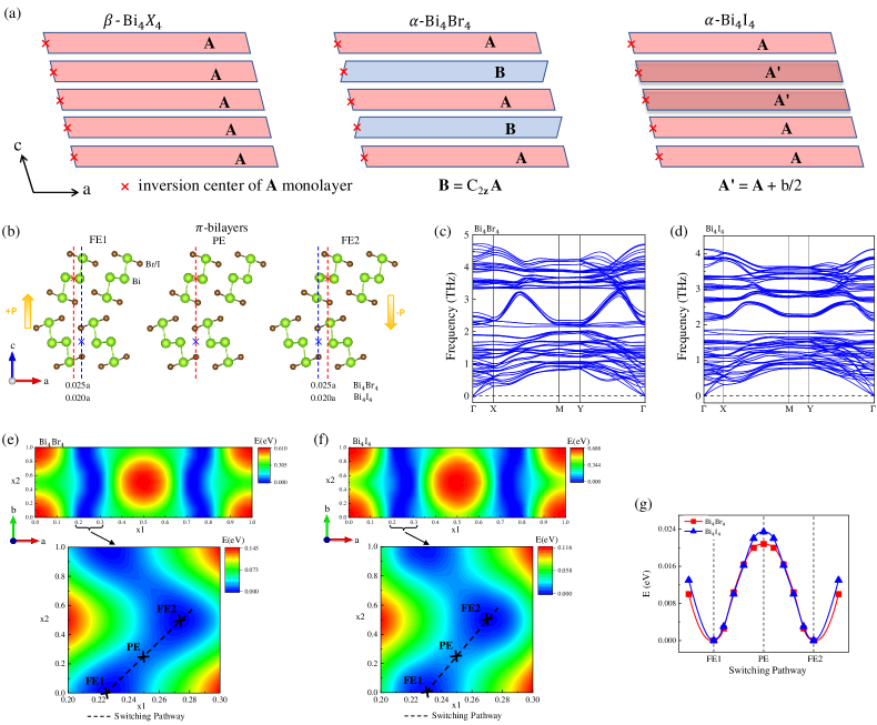
The 1T-Te2 monolayer possesses a hexagonal structure with space group (SG #164), where each atom lies at the center of an octahedral cage formed by Te atoms. IS forbids spontaneous polarization. As reported in Ref Wang et al. (2019), the two adjacent layers are related by rotation, and the only difference between Td and T0 phase MoTe2 is the interlayer shift, yielding ferroelectricity in the semimetal Td-MoTe2. We construct a bilayer system, where the top and bottom 1T monolayers ( plane) are related by rotation. The calculation details are given in Appendix A. Hereafter, starting from the centrosymmetric monolayer without symmetry, the -related bilayer system is called the bilayer, which breaks IS. The -bilayer structure can be widely found in nature materials, such as 1T′/Td/T0-TMD, -Bi (=Br, I). Note that the monolayer of the Td and T0 phase is identical. Exfoliated from the Td-MoTe2 bulk, we calculate the FE polarization of the metallic MoTe2 bilayer being 0.25 pC/m, where FE switching under the electric field can be easily achieved (Appendix B). In addition, the crystal structures, bilayers, and vertical polarization of topological compounds Bi are presented in detail in Appendix B.
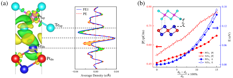
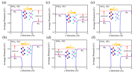
In the series of -bilayer structures, a glide symmetry (: mirror symmetry with a fractional in-plane translation) is preserved in the systems with , while others with do not have such a . The interlayer Te atoms distance of the bilayer is obtained by full relaxation. Its structure is parametrized by the (with respect to the lattice constants; ). The two FE phases with SG (#156) of PtTe2 are obtained in our calculations [FE1: ; FE2: ], whose structures are shown in Figs. 1(a) and 1(b). Because the two FE structures are related by , they have the opposite vertical polarizations. The vertical polarizations of Te2 FE bilayers are presented in Table 1. For the PtTe2 bilayer, the vertical polarization is 0.46 pC/m, comparable to that of the previous FEM WTe2 (0.40 pC/m) Fei et al. (2018); Qing et al. (2018). Due to the existence of symmetry, the net in-plane polarization is zero. The existence of vertical polarization is also confirmed by the discontinuity of vacuum levels on the upper and lower sides of the slab, details of which are shown in Appendix C. These results are consistent with the general theory for bilayer stacking ferroelectricity Ji et al. (2023).

| FE1 | P | Ebarrier | |
|---|---|---|---|
| PtTe2 | 0.46 | 2.67 | 56 |
| PdTe2 | 0.06 | 2.54 | 32 |
| NiTe2 | -0.52 | 2.66 | 22 |
II.2 Ferroelectric switching through interlayer sliding
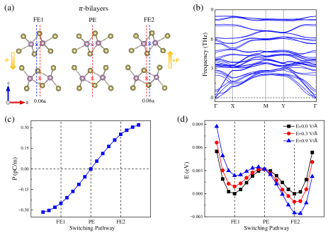
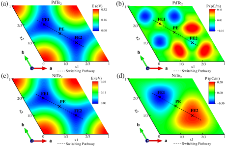
From the total energy and vertical polarization as a function of the in Figs. 1(c) and 1(e), we obtained an FE switching pathway realized by interlayer sliding as depicted by the dashed line. The energy barrier and polarization transition on the pathway are plotted in Figs. 1(d) and 1(f), respectively. As global ground states, two FE phases are dynamically stable, which is confirmed by phonon spectra in Fig. 2(a) for the PtTe2 FE bilayer. The phonon spectra of the PtTe2 paraelectric (PE) bilayer is presented in Fig. 2(b), with the vibration pattern of the B1 optical soft mode at point depicted in the inset. The PE phase [SG Aem2 (#39)] with at the saddle point of the energy surface is unstable and will spontaneously transition to two FE phases, which indicates that the PE phase is the transition state of the FE switching pathway.
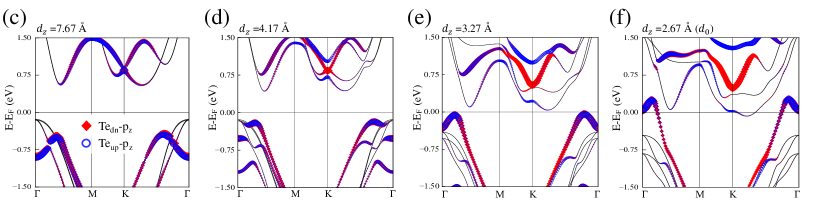
In addition, the typical energy double well structure is clearly visible in Fig. 1(d), with a low energy barrier of 56 meV per unit cell for the PtTe2 -bilayer, which is listed in Table 1. Such a low energy barrier is attributed to the fact that the interlayer sliding to achieve FE switching only needs to overcome weak interlayer vdW interactions, which does not involve the deformations of tightly bonded atoms as in displacive ferroelectrics Ding et al. (2017); Cohen (1992). Sliding driven the oscillation of interlayer potential can generate alternating current, which provides a platform for the development of a nanogenerator Lei and Menghao (2017); Qing et al. (2018). For PdTe2 and NiTe2 bilayers, contour plots of total energy and vertical polarization versus the can be found in Appendix C, which are similar to those of the PtTe2 bilayer.
II.3 Origin of vertical polarization
Interlayer sliding can be equivalent to rigid ion translation without vertical displacement, so vertical polarization is purely electronic in origin. We attribute the origin of polarization to the asymmetric charge density redistribution induced by interlayer vdW interactions, instead of the subtle ion displacement along the polarization direction from the inversion center as in displacive ferroelectrics represented by perovskite oxides Cohen (1992). In the FE1 phase of Fig. 3(a), the Te atom (Tedn) at the interface in the lower layer is directly below the Pt atom (Ptup) in the upper layer, while the Te atom (Teup) at the interface in the upper layer sits above the center of the triangle spanned by the Pt atom (Ptdn) in the lower layer. This asymmetric vdW stacking causes strong distortion of the spatially extended Tedn- orbital, making the interlayer vdW charge transfer near the Tedn atom significantly deviate from the symmetric distribution of the PE phase, as shown by the plane-averaged charge density difference along the direction in Fig. 3(a) for the PtTe2 bilayer. When the top layer slides along the switching pathway, the interlayer vdW charge transfer gradually reverses, resulting in the reversal of vertical polarization. Additionally, FE materials usually have a piezoelectric effect. By compressing in Fig. 3(b), vertical polarization can be further enhanced due to more intense vdW charge transfer.
II.4 Metallicity
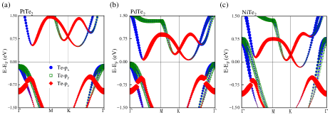
It is worth mentioning that the vdW charge transfer also introduces additional metallicity into our FE bilayers. Although the monolayer is insulating, the bilayer becomes metallic, which is further checked by the HSE06 functional (Appendix D). After the stacking, Teup and Tedn atoms lose electrons seriously due to the space expansion of the orbital, forming a large charge depletion zone like the orbital, as shown by the charge density difference in Fig. 3(a) for the PtTe2 bilayer. When the two monolayers are far apart in Fig. 3(c), the band structure can be regarded as a direct doubling of the band of monolayer (Appendix E). With the increase of the interlayer vdW charge transfer due to the reduced in Figs. 3(d)-3(f), the valence band dominated by Teup- and Tedn- orbitals gradually rise above near the point, moving the PtTe2 FE bilayer from an insulating phase to a metallic phase (see more in Appendix E).
In particular, the origin of metallicity of Te2 bilayers is different from that of the previous FEM WTe2 multilayers, where the centrosymmetric monolayer is already metallic Fei et al. (2018); Qing et al. (2018). In addition, by stacking 2D FE semiconductors to manipulate the depolarization field, it is possible to drive the inversion of the valence band maximum and the conduction band minimum, which is successful in introducing metallicity into the In ( = S, Se, and Te) FE system Ke et al. (2021). Electron doping is also an effective strategy. Very recently, by applying external gate bias to introduce free carriers, the coexistence of vertical polarization and in-plane conductance is realized in MoS2 and WSe2 insulated FE bilayers Deb et al. (2022).
II.5 Polarization versus doping
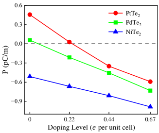
Next we will discuss the tunability of polarization in PtTe2-family bilayers through electron doping. Due to the metallic nature of FEMs, their carrier densities can be easily modified, and this can be simulated by replacing Te atoms with I atoms as electron doping. In Fig. 4, we simulate carrier densities regulation of polarization. The vertical polarization of the PtTe2 bilayer is shown to decrease to zero and then increase in the opposite direction with the increase of additional electrons. The magnitude of polarization reaches a maximum of 0.59 pC/m when doping 0.67 per unit cell, which is slightly larger than the original polarization of the PtTe2 bilayer. The introduction of effective electron doping in Te2 bilayers causes the negative charge centers to move upward relative to their positive charge centers. Recently, the full tunability of polarization by changing carrier densities in the FEM WTe2 bilayer is proved by experiments de la Barrera et al. (2021). Our results suggest that this ability to significantly adjust vertical polarization through charge carrier doping is a great advantage of Te2 FEMs and will be of great experimental interest.
III DISCUSSION
FEMs (or FE-like metals) are rare in nature but have demonstrated various fascinating properties, such as unconventional superconductivity Rischau et al. (2017); Saxena (2004), unique optical responses Mineev and Yoshioka (2010); Edelstein (2011), and magnetoelectric effects Edelstein (1995); Kanasugi and Yanase (2018). The vdW layered materials provide an ideal platform for the study of sliding and metallic ferroelectricity due to their unique interlayer interactions. In this work, we demonstrate that the series of PtTe2-family -bilayers are typical FEMs with significant adjustment of vertical polarization by changing carrier densities. First, we design the metallic -bilayer structure with vertical polarization by starting from centrosymmetric insulating 1T monolayers. Second, we show that the switching of vertical polarization is coupled with interlayer sliding, where a low energy barrier ensures high speed and energy-saving data storage and processing. Third, we explain that the polarization and metallicity are caused by charge density redistribution of the Te- orbital, induced by interlayer vdW interactions. Finally, we find that vertical polarization can be significantly adjusted in both magnitude and direction by doping I atoms, which is a advantage of Te2 FEMs. Electron doping causes the negative charge center to move upward relative to the positive charge center. These results predict a class of typical 2D FEMs, which have potential applications in functional nanodevices such as ferroelectric tunneling junction and nonvolatile ferroelectric memory. In addition, the bilayer of MoTe2 simultaneously exhibits ferroelectricity and superconductivity, which can be tuned by electron or hole doping. As the Bi monolayer is a quantum spin Hall insulator, the Bi bilayer would show both ferroelectricity and topology. In conclusion, the bilayer structure can be obtained in nature or in laboratory, which enables us to manipulate the interplay between the ferroelectricity and other properties, such as superconductivity and topology.
IV ACKNOWLEDGMENTS
We thank Professor Hongjun Xiang for helpful discussions. This work was supported by the National Key R&D Program of China (Grant No. 2022YFA1403800), the National Natural Science Foundation of China (Grants No. 11974395 and No. 12188101), the Strategic Priority Research Program of Chinese Academy of Sciences (Grant No. XDB33000000), and the Center for Materials Genome.
Appendix A CALCULATION AND METHODOLOGY
We carried out the first-principles calculations based on the density functional theory (DFT) with projector augmented wave (PAW) method Blöchl (1994); Kresse and Joubert (1999), as implemented in the Vienna ab initio simulation package (VASP) Kresse and Furthmüller (1996, 1996). The generalized gradient approximation (GGA) in the form of Perdew-Burke-Ernzerhof (PBE) function Perdew et al. (1996) was employed for the exchange-correlation potential. The kinetic energy cutoff for plane wave expansion was set to 500 eV, and a 18181 Monkhorst-Pack k-mesh was adopted for the Brillouin zone sampling in the self-consistent process. The first-order Methfessel-Paxton scheme with the width of the smearing 0.1 eV is used as the k-space integration/smearing method. The thickness of the vacuum layer along the axis was set to > 20 Å. Both lattice parameters and atomic positions were fully relaxed by minimizing the interionic forces below 10-2 eV/Å. The DFT-D3 method of Grimme with BJ damping was applied to consider vdW interaction Grimme et al. (2010, 2011). The dipole correction was applied in all calculations Neugebauer and Scheffler (1992). The Heyd–Scuseria–Ernzerhof (HSE06) hybrid functional Heyd et al. (2003) was employed to check band structure. An FE switching pathway was obtained with the climbing-image nudged elastic band method Henkelman et al. (2000). Phonon spectra were gained with the finite-difference method using a 331 supercell, as implemented in the Phonopy package Togo and Tanaka (2015).
Due to the disappearance of polarization uncertainty caused by the absence of periodicity in the out-of-plane direction, the vertical polarization of 2D systems is well defined by the classical dipole method Ding et al. (2017); Qing et al. (2018); Ma et al. (2021); Ke et al. (2021). The ion vertical polarization can be calculated by the point charge model, as shown in the following formula:
| (A1) |
where is the in-plane area of the unit cell, is the elementary charge, is the spatial position of the ion along the direction, is the ionic charge of the ion, is the total number of electrons, and represents the ion center (positive charge center) of the system in the direction. The sum is over all ions in the unit cell.
Because of the continuous distribution of electron cloud, the electron vertical polarization can be calculated using the following equation:
| (A2) |
where represents the electronic charge density, represents the electron center (negative charge center) of the system in the direction, and the integral is over the whole unit cell.
The total vertical polarization is the sum of the ion polarization and the electron polarization,
| (A3) |
where the direction is from the negative charge center to the positive charge center.
Appendix B FERROELECTRIC IN MoTe2 AND Bi BILAYERS
The 1T′-MoTe2 monolayer with SG (#11) hosts IS and lacks spontaneous polarization. We construct the -bilayer structure, which can be directly exfoliated from the 1T′/Td/T0-phases MoTe2 bulk Wang et al. (2019); Huang et al. (2019), to introduce ferroelectricity. As shown in Fig. 5(a), the two FE phases with SG (#6) and the PE phase with SG (#26) are obtained in our calculations [FE1: ; FE2: ; PE: ]. Because the two FE structures are related by symmetry, they have the opposite vertical polarizations (0.25 pC/m). A glide symmetry (: with a fractional in-plane translation) and symmetry in the PE phase forbid vertical polarization. As confirmed by phonon spectra in Fig. 5(b), the two FE phases are dynamically stable. The FE switching is realized by interlayer sliding. The polarization transition and energy barrier (under different vertical electric fields) on the FE switching pathway are plotted in Fig. 5(c) and 5(d), respectively. The typical energy double well is clearly visible, with a low energy barrier of 3.18 meV per unit cell. In addition, we investigate the influence of the external electric field perpendicular to the slab on the energy pathway of FE switching, where the vertical electric field is applied by introducing a dipole layer in the middle of the vacuum region Neugebauer and Scheffler (1992). With increasing the electric field in Fig. 5(d), the energy barrier from FE1 to FE2 decreases dramatically, which suggests that FE switching under the electric field can be easily achieved Ma et al. (2021).
The - and -Bi (=Br, I) crystal structures are shown in Fig. 6(a). Among them, the -Bi4Br4 crystallizes in the monoclinic SG (#12), where the two adjacent layers are related by rotation Noguchi et al. (2021). The Bi4Br4 monolayer, a large-gap quantum spin Hall insulator Zhou et al. (2014), hosts IS and lacks polarization. In order to introduce ferroelectricity, we construct the -bilayer structure. The two FE phases with SG (#8) and the PE phase with SG (#7) are obtained in our calculations [FE1: ; FE2: ; PE: ], whose structures are shown in Fig. 6(b). The two FE structures linked by symmetry have the opposite vertical polarizations (0.05 pC/m), and are dynamically stable, which is confirmed by phonon spectra in Fig. 6(c). A glide symmetry in the PE phase forbids vertical polarization. From the total energy as a function of the in Fig. 6(e), we obtained an FE switching pathway realized by interlayer sliding as depicted by the dashed line. The typical energy double well structure is clearly visible in Fig. 6(g), with a low energy barrier of 20.8 meV per unit cell. In addition, the Bi4I4 -bilayer with vertical polarizations of 0.24 pC/m has the same FE behaviors [FE1: ; FE2: ; PE: ], as shown in Figs. 6(d), 6(f), and 6(g).
Appendix C FERROELECTRIC IN Te2 BILAYERS
Due to the presence of spontaneous vertical polarization, there is a built-in electric field, resulting in different vacuum levels on the upper and lower sides of the FE slab. As shown by plane-averaged electrostatic potential along the direction in Fig. 7, the discontinuity of vacuum levels is obvious, where and represent the vacuum levels of the top and bottom sides, respectively. For PtTe2 bilayers in Figs. 7(a) and 7(b), the negative (-0.051 eV) of the FE1 phase indicates an upward vertical polarization, while a vertical polarization of the FE2 phase with equal magnitude and the opposite direction is demonstrated by the positive (0.051 eV) with equal magnitude. The same is true for PdTe2 and NiTe2 bilayers, as shown in Figs. 7(c)-7(f). The larger the , the greater the spontaneous polarization, which is also reflected in Te2 FE bilayers. Contour plots of total energy and vertical polarization versus the for PdTe2 and NiTe2 bilayers are shown in Fig. 8, which are similar to those of the PtTe2 bilayer.

Appendix D BAND STRUCTURE OF Te2
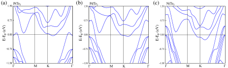
Orbital-resolved band structures for Te2 1T monolayers are shown in Fig. 9. In order to check the metallicity of Te2 FE bilayers, we employ the HSE06 functional to obtain more accurate band structures. As shown in Fig. 10, the bilayers are metallic, which is consistent with the results of the PBE functional [see Figs. 3(f), 11(d), and 11(h)]. The difference in band structure obtained by the HSE06 function and the PBE function is negligible.
Appendix E ORIGIN OF METALLICITY FOR PdTe2 AND NiTe2 BILAYERS
As with the PtTe2 FE bilayer described in the main text, interlayer vdW charge transfer also causes the valence band rise to introduce metallicity into PdTe2 and NiTe2 FE bilayers. With the increase of the interlayer vdW charge transfer due to the reduced in Fig. 11(a)-11(d), the valence band dominated by the Teup- and Tedn- orbitals gradually rises above near the point, which transforms the PdTe2 FE bilayer from an insulator to a metal. For the NiTe2 1T monolayer in Fig. 9(c), although there is a non-zero density of states near , only two isolated valence bands dominated by the Te- and Te- orbitals pass through , limiting conductivity. As shown in Figs. 11(e)-11(h), the same valence band rise gives the NiTe2 FE bilayer more conductive electron states.
References
- Valasek (1921) J. Valasek, Phys. Rev. 17, 475 (1921).
- Shen et al. (2019) X.-W. Shen, Y.-W. Fang, B.-B. Tian, and C.-G. Duan, ACS Applied Electronic Materials 1, 1133 (2019).
- Yuan et al. (2019) S. Yuan, X. Luo, H. L. Chan, C. Xiao, Y. Dai, M. Xie, and J. Hao, Nature Communications 10, 1775 (2019).
- Ding et al. (2017) W. Ding, J. Zhu, Z. Wang, Y. Gao, D. Xiao, Y. Gu, Z. Zhang, and W. Zhu, Nature Communications 8, 14956 (2017).
- Fei et al. (2016) R. Fei, W. Kang, and L. Yang, Phys. Rev. Lett. 117, 097601 (2016).
- Qi et al. (2021) L. Qi, S. Ruan, and Y.-J. Zeng, Advanced Materials 33, 2005098 (2021).
- Chanana and Waghmare (2019) A. Chanana and U. V. Waghmare, Phys. Rev. Lett. 123, 037601 (2019).
- Manzeli et al. (2017) S. Manzeli, D. Ovchinnikov, D. Pasquier, O. V. Yazyev, and A. Kis, Nature Reviews Materials 2, 17033 (2017).
- Yin et al. (2021) X. Yin, C. S. Tang, Y. Zheng, J. Gao, J. Wu, H. Zhang, M. Chhowalla, W. Chen, and A. T. S. Wee, Chem. Soc. Rev. 50, 10087 (2021).
- Novoselov et al. (2004) K. S. Novoselov, A. K. Geim, S. V. Morozov, D. Jiang, Y. Zhang, S. V. Dubonos, I. V. Grigorieva, and A. A. Firsov, Science 306, 666 (2004).
- Tavakoli et al. (2021) M. M. Tavakoli, J.-H. Park, J. Mwaura, M. Saravanapavanantham, V. Bulović, and J. Kong, Advanced Functional Materials 31, 2101238 (2021).
- Lei and Menghao (2017) L. Lei and W. Menghao, ACS Nano 11, 6382–6388 (2017).
- Zhong et al. (2021) T. Zhong, Y. Ren, Z. Zhang, J. Gao, and M. Wu, J. Mater. Chem. A 9, 19659 (2021).
- Xiao et al. (2022) R.-C. Xiao, Y. Gao, H. Jiang, W. Gan, C. Zhang, and H. Li, npj Computational Materials 8, 138 (2022).
- Sun et al. (2022) W. Sun, W. Wang, H. Li, X. Li, Z. Yu, Y. Bai, G. Zhang, and Z. Cheng, npj Computational Materials 8, 159 (2022).
- Zhang et al. (2022) T. Zhang, X. Xu, B. Huang, Y. Dai, and Y. Ma, npj Computational Materials 8, 64 (2022).
- Liu et al. (2020) X. Liu, A. P. Pyatakov, and W. Ren, Phys. Rev. Lett. 125, 247601 (2020).
- Yasuda et al. (2021) K. Yasuda, X. Wang, K. Watanabe, T. Taniguchi, and P. Jarillo-Herrero, Science 372, 1458 (2021).
- Stern et al. (2021) M. V. Stern, Y. Waschitz, W. Cao, I. Nevo, K. Watanabe, T. Taniguchi, E. Sela, M. Urbakh, O. Hod, and M. B. Shalom, Science 372, 1462 (2021).
- Wang et al. (2022) X. Wang, K. Yasuda, Y. Zhang, S. Liu, K. Watanabe, T. Taniguchi, J. Hone, L. Fu, and P. Jarillo-Herrero, Nature Nanotechnology 17, 367 (2022).
- Meng et al. (2022) P. Meng, Y. Wu, R. Bian, E. Pan, B. Dong, X. Zhao, J. Chen, L. Wu, Y. Sun, Q. Fu, Q. Liu, D. Shi, Q. Zhang, Y.-W. Zhang, Z. Liu, and F. Liu, Nature Communications 13, 7696 (2022).
- Deb et al. (2022) S. Deb, W. Cao, N. Raab, K. Watanabe, T. Taniguchi, M. Goldstein, L. Kronik, M. Urbakh, O. Hod, and M. Ben Shalom, Nature 612, 465 (2022).
- Fei et al. (2018) Z. Fei, W. Zhao, T. A. Palomaki, B. Sun, M. K. Miller, Z. Zhao, J. Yan, X. Xu, and D. H. Cobden, Nature 560, 336 (2018).
- Qing et al. (2018) Y. Qing, M. Wu, and L. Ju, J. Phys. Chem. Lett. 9, 7160–7164 (2018).
- Xiao et al. (2020) J. Xiao, Y. Wang, H. Wang, C. D. Pemmaraju, S. Wang, P. Muscher, E. J. Sie, C. M. Nyby, T. P. Devereaux, X. Qian, X. Zhang, and A. M. Lindenberg, Nature Physics 16, 1028 (2020).
- Wan et al. (2022) Y. Wan, T. Hu, X. Mao, J. Fu, K. Yuan, Y. Song, X. Gan, X. Xu, M. Xue, X. Cheng, C. Huang, J. Yang, L. Dai, H. Zeng, and E. Kan, Phys. Rev. Lett. 128, 067601 (2022).
- Jindal et al. (2023) A. Jindal, A. Saha, Z. Li, T. Taniguchi, K. Watanabe, J. C. Hone, T. Birol, R. M. Fernandes, C. R. Dean, A. N. Pasupathy, and D. A. Rhodes, Nature 613, 48 (2023).
- Ji et al. (2023) J. Ji, G. Yu, C. Xu, and H. J. Xiang, Phys. Rev. Lett. 130, 146801 (2023).
- Anderson and Blount (1965) P. W. Anderson and E. I. Blount, Phys. Rev. Lett. 14, 217 (1965).
- Shi et al. (2013) Y. Shi, Y. Guo, X. Wang, A. J. Princep, D. Khalyavin, P. Manuel, Y. Michiue, A. Sato, K. Tsuda, S. Yu, M. Arai, Y. Shirako, M. Akaogi, N. Wang, K. Yamaura, and A. T. Boothroyd, Nature Materials 12, 1024 (2013).
- Xiang (2014) H. J. Xiang, Phys. Rev. B 90, 094108 (2014).
- Rischau et al. (2017) C. W. Rischau, X. Lin, C. P. Grams, D. Finck, S. Harms, J. Engelmayer, T. Lorenz, Y. Gallais, B. Fauqué, J. Hemberger, and K. Behnia, Nature Physics 13, 643 (2017).
- Enderlein et al. (2020) C. Enderlein, J. F. de Oliveira, D. A. Tompsett, E. B. Saitovitch, S. S. Saxena, G. G. Lonzarich, and S. E. Rowley, Nature Communications 11, 4852 (2020).
- Cai et al. (2021) W. Cai, J. He, H. Li, R. Zhang, D. Zhang, D. Y. Chung, T. Bhowmick, C. Wolverton, M. G. Kanatzidis, and S. Deemyad, Nature Communications 12, 1509 (2021).
- Wang et al. (2019) Z. Wang, B. J. Wieder, J. Li, B. Yan, and B. A. Bernevig, Phys. Rev. Lett. 123, 186401 (2019).
- Huang et al. (2019) F.-T. Huang, S. Joon Lim, S. Singh, J. Kim, L. Zhang, J.-W. Kim, M.-W. Chu, K. M. Rabe, D. Vanderbilt, and S.-W. Cheong, Nature Communications 10, 4211 (2019).
- Luo et al. (2017) W. Luo, K. Xu, and H. Xiang, Phys. Rev. B 96, 235415 (2017).
- Lu et al. (2019) J. Lu, G. Chen, W. Luo, J. Íñiguez, L. Bellaiche, and H. Xiang, Phys. Rev. Lett. 122, 227601 (2019).
- Ma et al. (2021) X.-Y. Ma, H.-Y. Lyu, K.-R. Hao, Y.-M. Zhao, X. Qian, Q.-B. Yan, and G. Su, Science Bulletin 66, 233 (2021).
- de la Barrera et al. (2021) S. C. de la Barrera, Q. Cao, Y. Gao, Y. Gao, V. S. Bheemarasetty, J. Yan, D. G. Mandrus, W. Zhu, D. Xiao, and B. M. Hunt, Nature Communications 12, 5298 (2021).
- Cohen (1992) R. E. Cohen, Nature 358, 136 (1992).
- Ke et al. (2021) C. Ke, J. Huang, and S. Liu, Mater. Horiz. 8, 3387 (2021).
- Saxena (2004) P. Saxena, S.and Monthoux, Nature 427, 799 (2004).
- Mineev and Yoshioka (2010) V. P. Mineev and Y. Yoshioka, Phys. Rev. B 81, 094525 (2010).
- Edelstein (2011) V. M. Edelstein, Phys. Rev. B 83, 113109 (2011).
- Edelstein (1995) V. M. Edelstein, Phys. Rev. Lett. 75, 2004 (1995).
- Kanasugi and Yanase (2018) S. Kanasugi and Y. Yanase, Phys. Rev. B 98, 024521 (2018).
- Blöchl (1994) P. E. Blöchl, Phys. Rev. B 50, 17953 (1994).
- Kresse and Joubert (1999) G. Kresse and D. Joubert, Phys. Rev. B 59, 1758 (1999).
- Kresse and Furthmüller (1996) G. Kresse and J. Furthmüller, Computational Materials Science 6, 15 (1996).
- Kresse and Furthmüller (1996) G. Kresse and J. Furthmüller, Phys. Rev. B 54, 11169 (1996).
- Perdew et al. (1996) J. P. Perdew, K. Burke, and M. Ernzerhof, Phys. Rev. Lett. 77, 3865 (1996).
- Grimme et al. (2010) S. Grimme, J. Antony, S. Ehrlich, and H. Krieg, The Journal of Chemical Physics 132, 154104 (2010).
- Grimme et al. (2011) S. Grimme, S. Ehrlich, and L. Goerigk, Journal of Computational Chemistry 32, 1456 (2011).
- Neugebauer and Scheffler (1992) J. Neugebauer and M. Scheffler, Phys. Rev. B 46, 16067 (1992).
- Heyd et al. (2003) J. Heyd, G. E. Scuseria, and M. Ernzerhof, The Journal of Chemical Physics 118, 8207 (2003).
- Henkelman et al. (2000) G. Henkelman, B. P. Uberuaga, and H. Jónsson, The Journal of Chemical Physics 113, 9901 (2000).
- Togo and Tanaka (2015) A. Togo and I. Tanaka, Scripta Materialia 108, 1 (2015).
- Noguchi et al. (2021) R. Noguchi, M. Kobayashi, Z. Jiang, K. Kuroda, T. Takahashi, Z. Xu, D. Lee, M. Hirayama, M. Ochi, T. Shirasawa, P. Zhang, C. Lin, C. Bareille, S. Sakuragi, H. Tanaka, S. Kunisada, K. Kurokawa, K. Yaji, A. Harasawa, V. Kandyba, A. Giampietri, A. Barinov, T. K. Kim, C. Cacho, M. Hashimoto, D. Lu, S. Shin, R. Arita, K. Lai, T. Sasagawa, and T. Kondo, Nature Materials 20, 473 (2021).
- Zhou et al. (2014) J.-J. Zhou, W. Feng, C.-C. Liu, S. Guan, and Y. Yao, Nano Letters 14, 4767 (2014), pMID: 25058154, https://doi.org/10.1021/nl501907g .