From Clean Room to Machine Room: Commissioning of the First-Generation BrainScaleS Wafer-Scale Neuromorphic System
Abstract
The first-generation of BrainScaleS, also referred to as BrainScaleS-1, is a neuromorphic system for emulating large-scale networks of spiking neurons. Following a “physical modeling” principle, its VLSI circuits are designed to emulate the dynamics of biological examples: analog circuits implement neurons and synapses with time constants that arise from their electronic components’ intrinsic properties. It operates in continuous time, with dynamics typically matching an acceleration factor of compared to the biological regime. A fault-tolerant design allows it to achieve wafer-scale integration despite unavoidable analog variability and component failures. In this paper, we present the commissioning process of a BrainScaleS-1 wafer module, providing a short description of the system’s physical components, illustrating the steps taken during its assembly and the measures taken to operate it. Furthermore, we reflect on the system’s development process and the lessons learned to conclude with a demonstration of its functionality by emulating a wafer-scale synchronous firing chain, the largest spiking network emulation ran with analog components and individual synapses to date.
Index Terms:
Neuromorphic hardware, wafer-scale integration, spiking neural networks, emulated networks, analog neuromorphic devices, synfire chains.I Introduction
Simulating the dynamic properties of large-scale spiking neural networks is challenging due to the massively parallel interactions of their neurons and synapses. The BrainScaleS neuromorphic architecture proposes a solution to this dilemma by providing inherently parallel computation at nodes operating as neurons and synapses and communicating through asynchronous spikes. It thereby achieves a constant emulation speed with increasing network sizes [1].
BrainScaleS implements physical models of neurons and synapses on a CMOS substrate with analog circuits, while the spike communication is digital. On the one hand, the physical models inherently provide solutions to neuron and synapse dynamics in continuous time, in contrast to the time-discretized and numerically integrated solutions of digital systems and software simulations. On the other hand, the programmable digital communication of action potentials allows for flexible network topologies and the possibility of using digital logic to feed and read spike events from outside the system. Furthermore, circuits are operated in strong inversion, targeting dynamics with a typical speedup factor of compared to biological real-time.
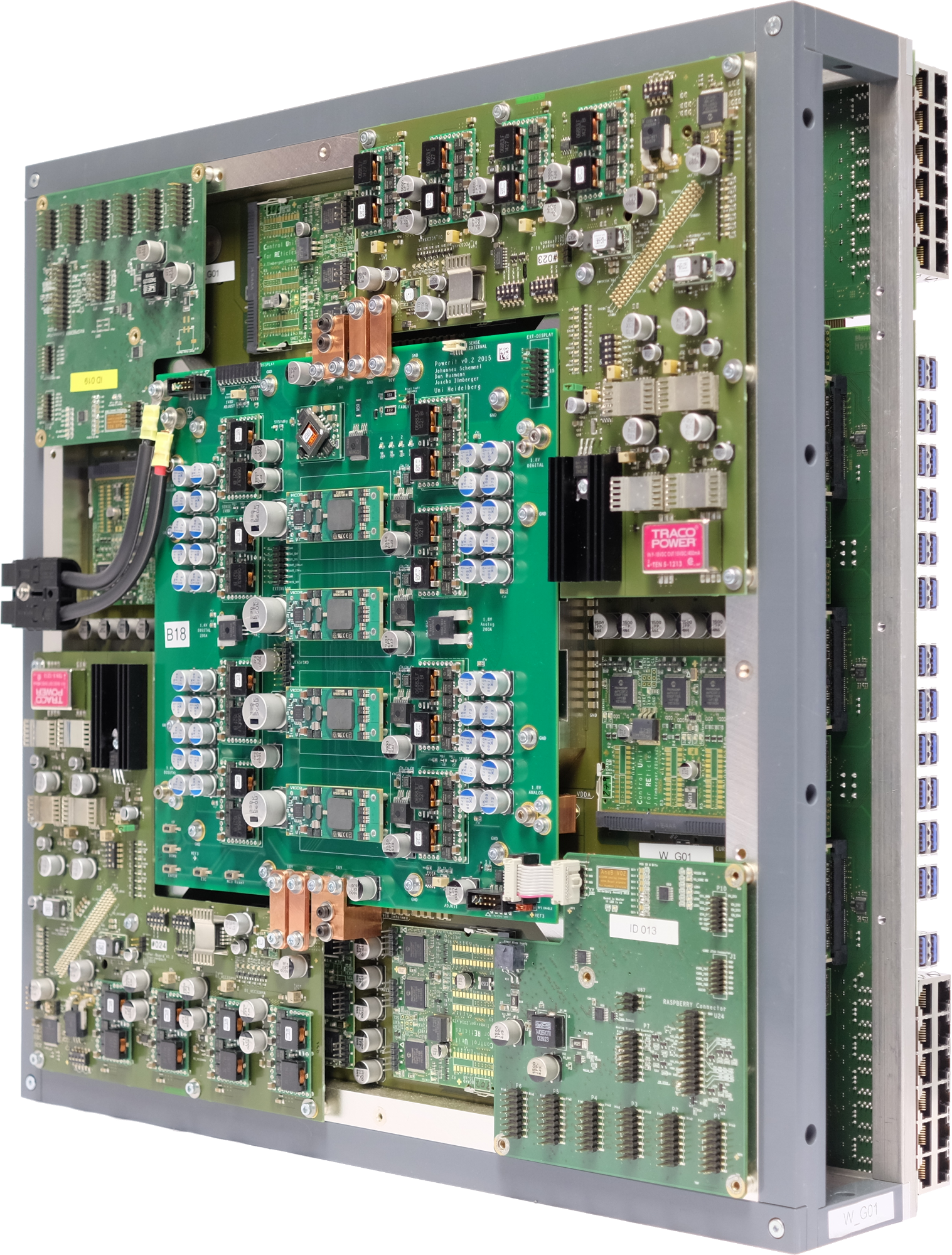
The BrainScaleS-1 system utilizes wafer-scale integration to achieve large ASIC counts with energy efficiency and high communication bandwidth. The structure of its underlying neuromorphic chip and the technology to achieve its wafer-scale integration are introduced in [2, 3, 4, 5]. Turning the silicon wafer into a ready-to-use system, though, implicates bringing several additional components, shown in fig. 1, to work hand in hand. For that cause, a commissioning chain is established, which is this paper’s focus.
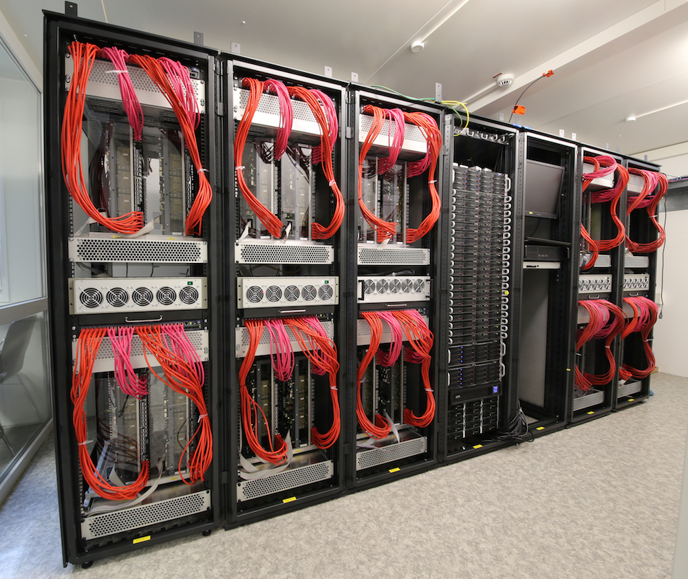
We first illustrate the different components that constitute the system and how they are tested. Then, we show the steps to assemble the module before it is finally placed in the machine room, as shown in fig. 2. In the second part of the paper, we describe the methods devised to bring such a system into a reliable substrate for neuromorphic experiments: a large number of VLSI analog components inevitably leads to malfunctioning parts and analog variability, for which an underlying fault-tolerant design and suitable handling have to be put in place. To demonstrate its operation and the successful implementation of these measures, a biologically-motivated network of spiking neurons, a synchronous firing chain, is emulated on a fully commissioned BrainScaleS-1 wafer module.
The system belongs to the still-nascent field of neuromorphic computing and remains under continuous development. Having pioneered a neuromorphic wafer-scale integration of VLSI analog and digital circuits, we also discuss the lessons learned while solving or circumventing the challenges faced along the way.
II System Components and Individual Tests
A BrainScaleS-1 wafer module is depicted in fig. 1. Each of its constituent boards is individually tested before its integration into the system, which permits differentiating errors in the parts from those arising from the assembly. A short description of each component and the tests it undergoes is given in the following.
II-A The BrainScaleS-1 Wafer
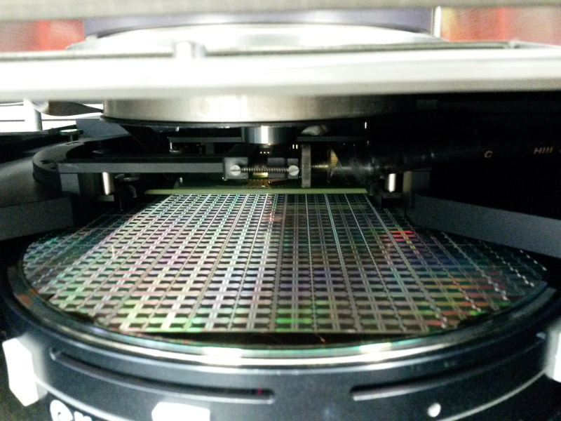
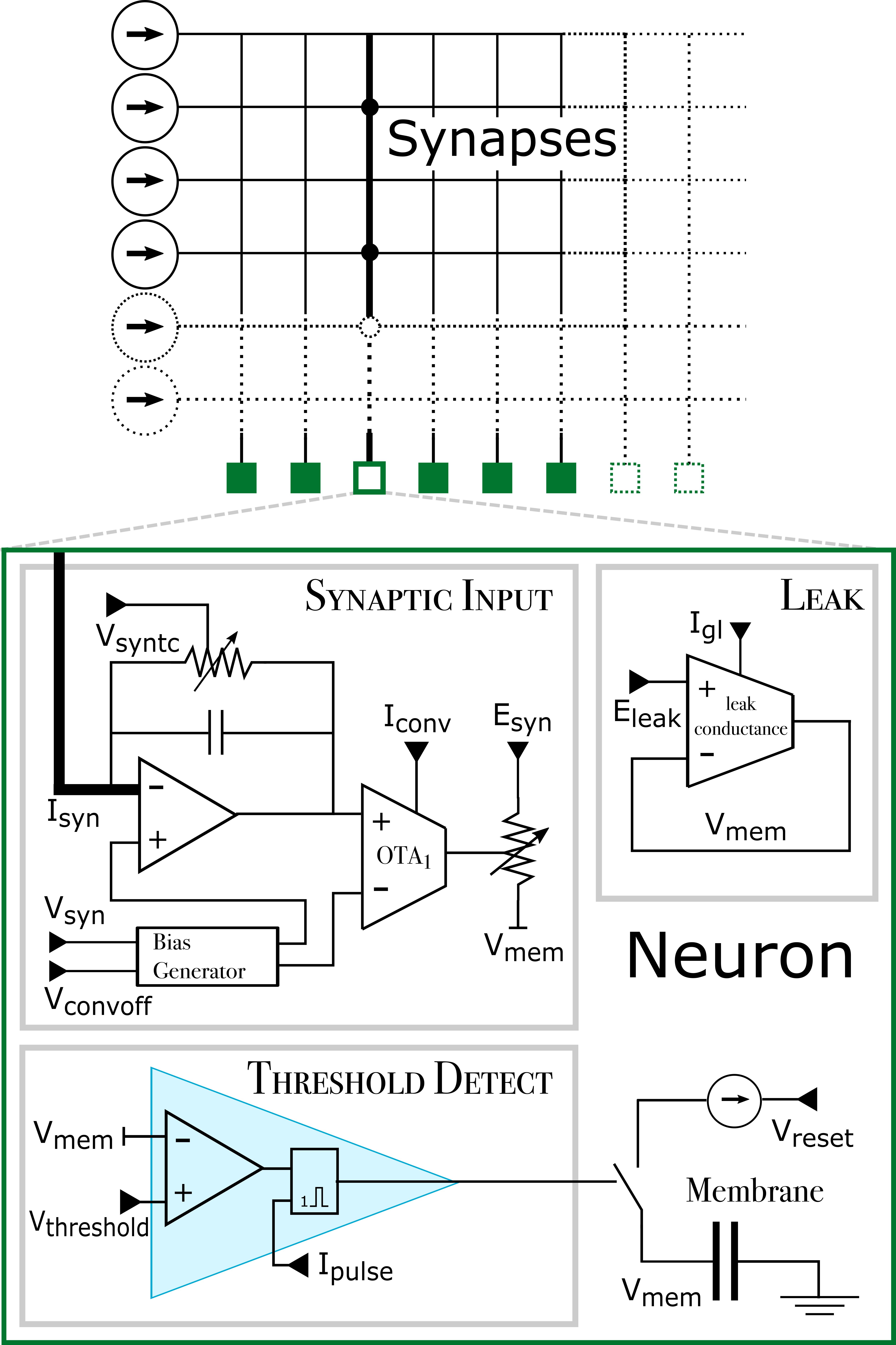
The heart of each module is an uncut wafer, displayed in fig. 3a, fabricated in UMC technology comprising 384 High Input Count Analog Neural Network (HICANN) ASICs. Each HICANN contains analog neuron circuits implementing the adaptive exponential integrate-and-fire (AdEx) model [5]. Single neuron circuits receive input from up to analog synapses. Since neuron membranes can interconnect in groups of up to , a maximum of synapses can provide input to each of these composite neurons. Synapse weights are stored with -bit resolution in local SRAM at each synapse.
Each HICANN stores analog quantities for parameterization of its analog circuits in Single-Poly Floating Gate (FG) CMOS cells that retain their operation levels according to their isolated gate’s accumulated charge [7, 8].
These FGs are written via an onboard -bit-resolution DAC, enabling reprogramming via incremental loops with feedback.
Then, the stored values get translated to either a voltage or a current using a source follower or a current mirror, respectively, to set neuron parameters and other onboard circuit operation levels.
While these FGs present a low-power, small-space solution to store analog operation settings, they introduce write-cycle to write-cycle variability, as will be further discussed.
Wafer-wide communication is achieved with a custom-developed redistribution layer applied post-wafer-production, creating around lateral connections across chip borders [9].
These connections provide the modules with on-wafer spike event communication through low-voltage differential signaling (LVDS) buses utilizing an asynchronous serial event transmission protocol.
Furthermore, connections through top-layer pads on the wafer provide the modules with parallel per HICANN off-wafer communication, which in conjunction with programmable and redundant components, constitute the system’s fault tolerance [2].
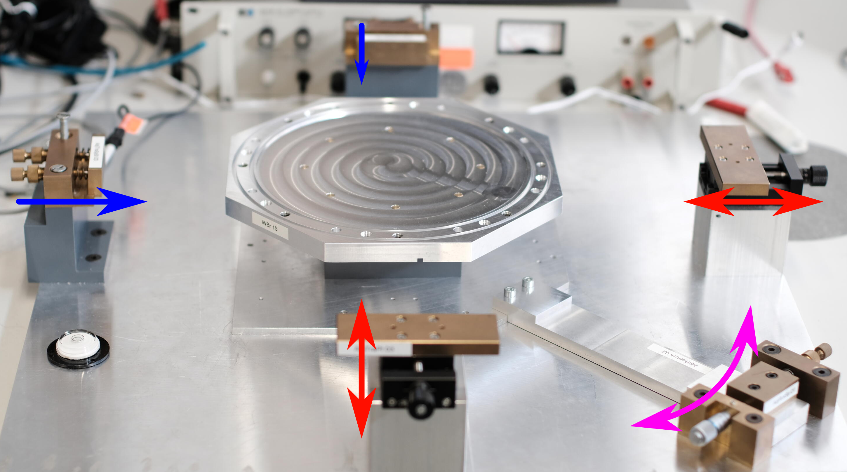
Testing: In order to assess the effect of wafer post-processing on the digital yield of an entire wafer, initial needle card tests were carried out on two unprocessed111”unprocessed” in this context means untested wafers straight from the manufacturer, before the custom redistribution layers have been added. wafers to determine their yield immediately after production. Since the wafers undergoing these tests cannot be further processed, comparing results on the same wafers before and after the post-processing is, however, not possible.
The setup for these tests in the institute’s clean room is shown in fig. 4, and the procedure is as follows. The needle card is used to contact each individual ASIC. Immediately after contacting and powering up, the total current on the used lab supply is measured to detect potential power shorts. Henceforward, all digital memory cells on the HICANN circuits are tested using a built-in Joint Test Action Group (JTAG) access mode. During these tests, HICANNs on each of the two wafers were tested, and of them showed no single digital error. To compare, UMC’s calculator estimates a yield of approximately by taking into account the process parameters and circuit size. However, our results are only an estimation: On the one hand, the tested digital memory cells only cover a fraction of the whole silicon area, which is dominated by analog circuitry. Therefore, the digital test yield could be assumed to be too optimistic. On the other hand, perfect power and signal integrity could not be ensured while connecting the circuits through the needles, leading to a possible detection of false negatives, caused for example by slightly underpowered memory cells. In addition, only wafers from the initial engineering sample production have been available for testing. No documentation has been available to relate the production yield data from UMC to small batch-size engineering runs. Nonetheless, the results match the expectations taking the high level of uncertainty into account. Also, a yield in the order of, e.g., would not indicate that of the dies cannot be used. Instead, advantaging from the fault-tolerant design, and depending on the defect type, it could suffice to disable single neuron or synapse circuits, for example, on affected HICANNs that are otherwise fully functional and can remain available for experiments.
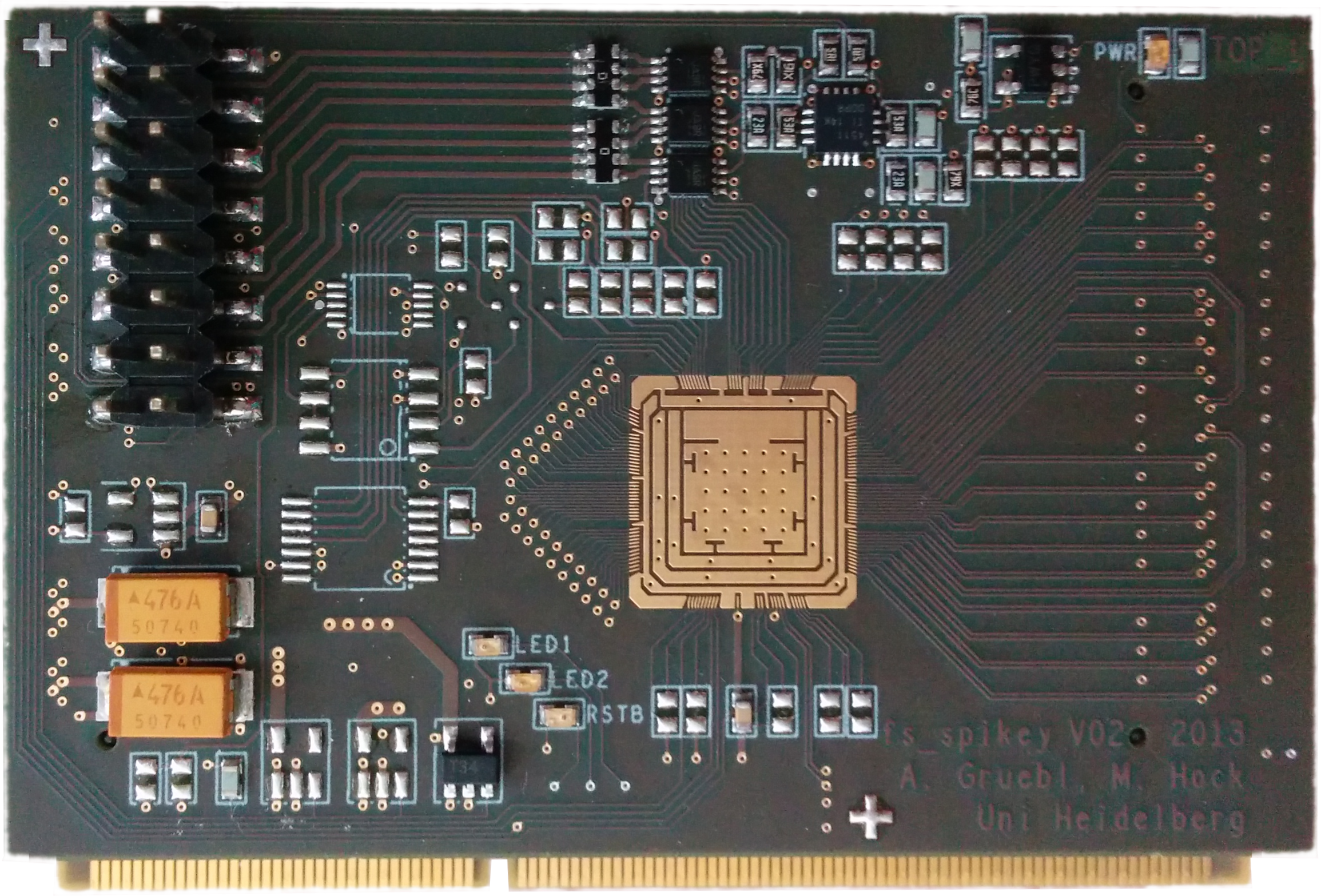
II-B Main PCB
The Main PCB, displayed in fig. 3b, is a passive interconnector board for most parts of the wafer-scale integration system. Seven of its layers are used to distribute power rails carrying up to of current. The rest of the layers are used to route power monitoring, high-speed differential communication, and different sideband signals. Auxiliary boards, communication infrastructure, and the silicon wafer are connected via various kinds of detachable connectors. These enable system modularity for development and upgrades, desirable for research and development in dynamic environments over longer timespans.
Testing: The manufacturer222Manufactured by Würth Elektronik, Germany performs complete optical inspection and electrical tests of the Main PCB. The BrainScaleS-1 wafer modules are assembled using exclusively fully validated, error-free Main PCBs.
II-C Auxiliary Boards
The wafer module is completed by populating it with communication boards and auxiliary boards for power delivery, control, monitoring, and inter-module communication.
II-C1 Communication Boards
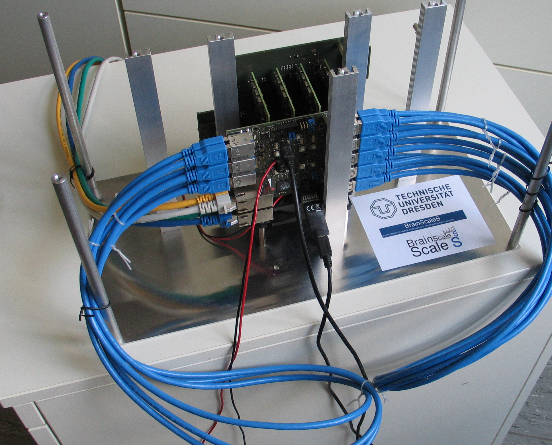
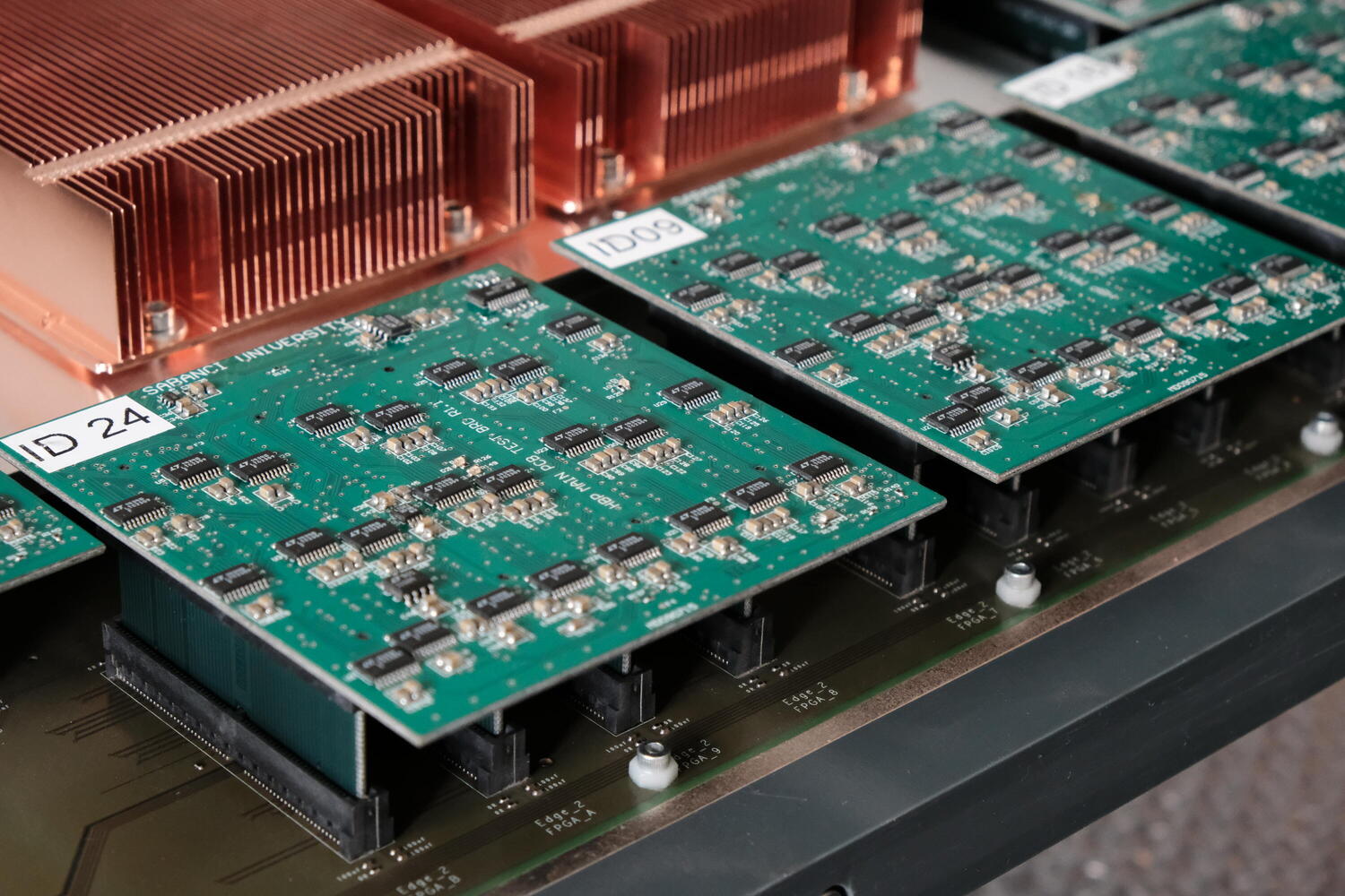
Each communication board333Developed at the chair of Hochparallele VLSI-Systeme und Neuromikroelektronik at TU Dresden contains a field-programmable gate array (FPGA) and connects to one HICANN group consisting of HICANNs . These boards communicate through separate high-speed LVDS interfaces with each of the connected HICANNs to configure, monitor, and coordinate the experiment runs; they feed and collect generated spikes into/from the experiments. Furthermore, they synchronize the start of experiments to allow for wafer wide execution. Trigger signals generated on these boards also align experiments with analog recordings using the Analog Readout Module (AnaRM) .
Testing: The communication boards are tested on a standalone setup that implements loopback connections for the high-speed interfaces. For this purpose, a test board accommodates and tests four PCBs in parallel, as shown in fig. 5a. Primarily automated and controlled via software, the tests switch the power supply via General Purpose Interface Bus (GPIB) . Programming is performed via JTAG and Power Management Bus (PMBus) . Tests comprising current consumption measurements, loading and communicating with the FPGA design, as well as memory tests are conducted. In addition, communication with the host computer as well as the links to the wafer and neighboring communication boards are tested. As per data logs, only out of produced PCBs had to be discarded after failed tests.
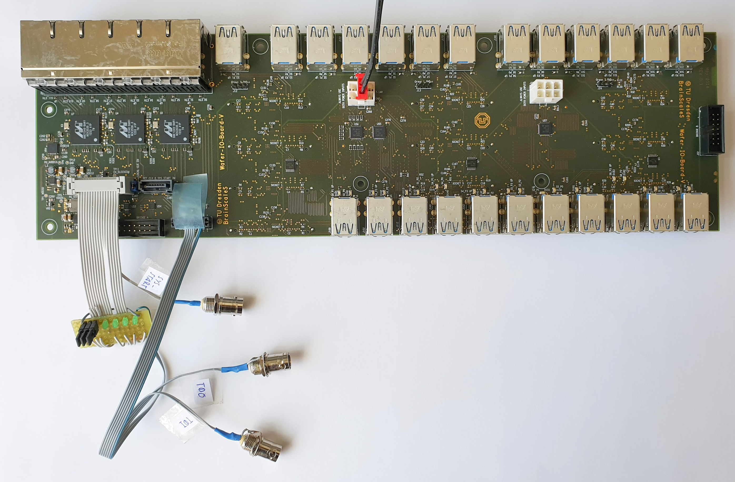
II-C2 Wafer I/O PCB
Each one of the module’s four Wafer I/O PCBs (WIOs) 3 attaches to twelve communication boards, aggregating Gbit-Ethernet and connections to other communication boards.
Testing: A manual approach is followed as the number of boards is smaller than that of the communication boards. The board, shown in fig. 5b, is supplied with power, and the proper functioning of the DC/DC converters is checked with a multimeter. Individual communication ports are tested. In addition, the proper transmission of signals using a signal generator and differential probes is measured. A partial test of the JTAG pins is also carried out. As per data logs, only out of produced WIOs were discarded after failed tests.
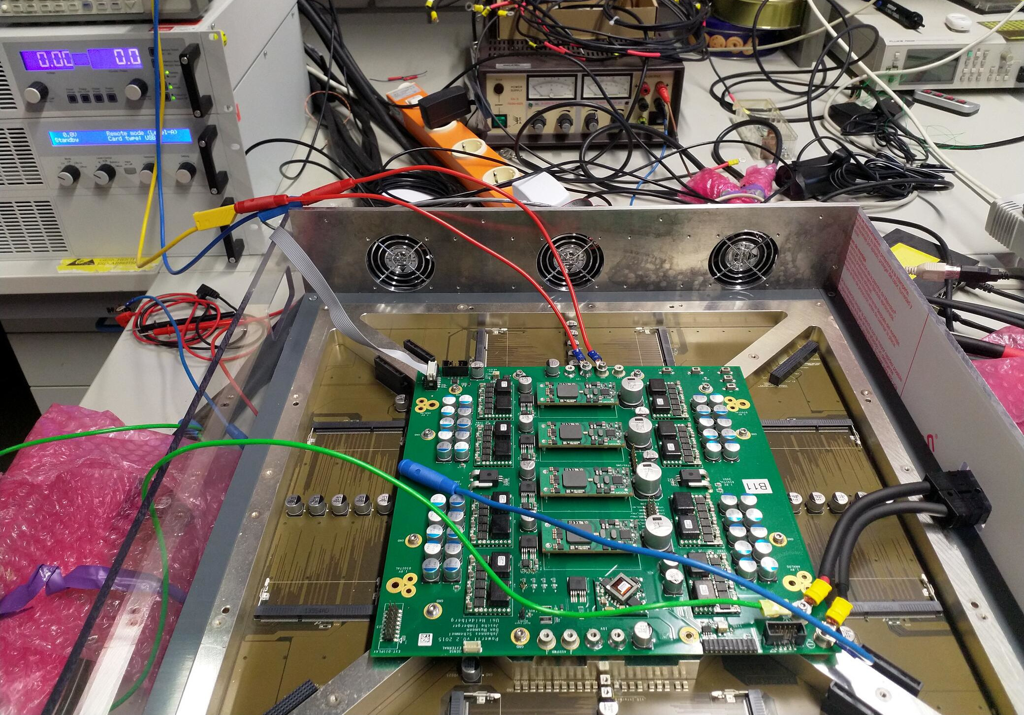
II-C3 Main Power Supply
The Main Power Supply (PowerIt) has three output channels: Two outputs as main analog and digital supplies of the wafer with a current limit of each, as well as a output capable of up to to supply the communication boards. Multiple custom-milled copper parts ensure a low-resistance screw connection between the PowerIt and the Main PCB. Additionally, digital control of the voltages and sensors as near to the wafer as possible allow for compensation of IR-drop. An integrated microcontroller can measure input and output currents and voltages via shunt resistors, hall sensors, and voltage dividers.
Testing: Commissioning of the PowerIt involves basic functionality tests and calibration of the current and voltage measurement circuits using an external electronic load capable of sinking and precision multimeters, see fig. 5c.

II-C4 Auxiliary Power Supply
The Auxiliary Power Supply PCB (AuxPwr) designed in [10], receives from the PowerIt and provides ten different voltage outputs for the wafer module. The currents drawn at the derived voltages vary from , for the common-mode voltage of the LVDS on-wafer communication, to for the synapse driver output. The board has an L-shape with linear and switching regulators placed on different axes to reduce the coils’ electromagnetic-noise induction. In addition, the usage of intermediate voltages reduces the power dissipation for the voltage scaling. An onboard microcontroller monitors all the voltages and currents. Four voltages can be controlled digitally through the Inter-Integrated Circuit (I2C) protocol.
Testing: The AuxPwr components’ functionality is tested during the calibration process of the board, during which an external voltmeter permits adjusting voltage offsets. A two-point linear calibration under load is performed for the currents. The test stand can be seen in fig. 5d.
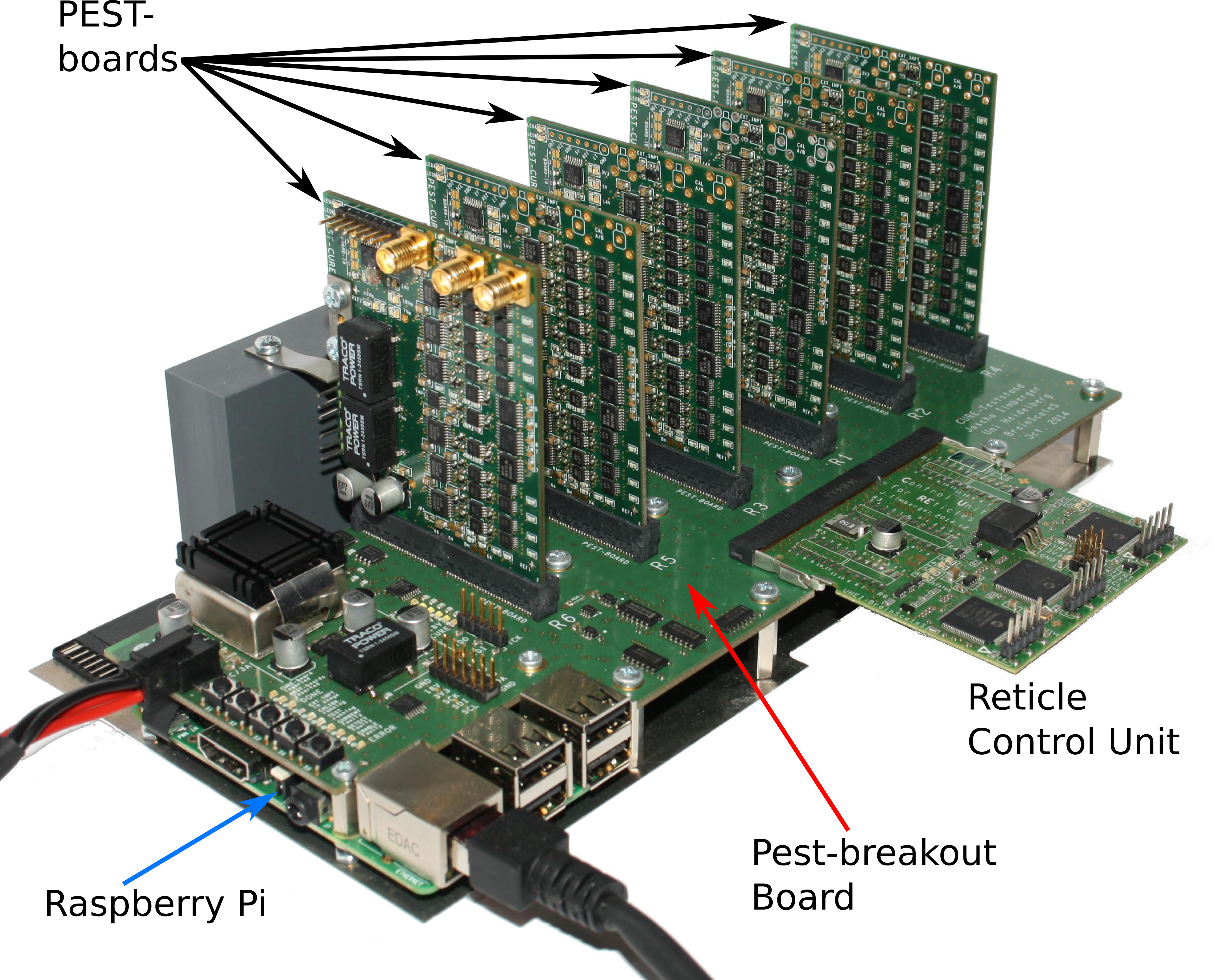
II-C5 Control Unit for Reticles
Since the BrainScaleS-1 wafer is not cut into individual chips, the wafer module must be fault-tolerant to individual HICANN problems. For this purpose, the Main PCB features power-FETs for the supply rails of each HICANN group of the wafer; overcurrents manifest as a large voltage drop across these power transistors. The Control Unit for Reticles (CURe) controls the gates of these transistors and monitors the supply voltages of the wafer. Three microcontrollers manage the measured data and react to fault conditions by shutting off the power of the affected HICANN groups. Thus, the CURe allows to identify individual fatal faults and to exclude the respective HICANN groups from the usable components. The term reticle refers to the semiconductor manufacturing process and consists of one HICANN group.
Testing: The CURe is tested using a custom setup producing the voltages expected inside the actual BrainScaleS-1 wafer module, simulating all possible fault conditions while the response time is measured. Likewise, the drive strength of the control signals for the power transistors on the Main PCB is quantified. The test setup is displayed in fig. 5e.
II-C6 Analog Readout Module
Further insight into the neuron dynamics can be obtained via measurements of its membrane potential, allowing for a better understanding of experiment results and the implementation of calibration routines. To this end, each neuron contains a switchable analog output amplifier that connects to one of two output buffers per die. These two outputs are each short-circuited across dies in the same HICANN group. Therefore, each of these groups has two analog outputs, totaling independent analog channels available on each wafer module.
The AnaRM system consists of twelve FPGA -controlled -bit ADC modules that allow for the digitization of the membrane voltages on one wafer module per BrainScaleS-1 system rack. Each of the modules in the AnaRM system connects through a ribbon cable to one of two Analog Breakout PCBs (AnaBs) mounted on the Main PCB, receiving eight analog signals that are multiplexed into the ADC. An additional digital signal acts as a trigger; four HICANN groups share one, allowing synchronization during an experiment between the involved communication boards, HICANNs and the AnaRM system. Overall, the AnaRM system can simultaneously sample 12 membrane traces per wafer module.
Testing: The FPGA board in the AnaRM , displayed in fig. 5f, undergoes DRAM memory tests and basic functional testing of all its peripheral components. The analog front end is tested during the calibration of the modules. This calibration is performed using a source meter to generate a series of ground-truth voltages, which are subsequently measured using each input channel. A series impedance is used at the output of the source meter to match the impedance of the output buffers on the HICANN . This voltage divider formed by the output and input impedances halves the span of the HICANN output to the maximum input of the AnaRM . A linear function fits the recorded signal to the source meter voltages, and the per board offset and gains are stored in a database.
II-D Main Control Unit
The Main Control Unit (MaCU) consists of a Raspberry Pi powered by the standby voltage of the PowerIt . Using the I2C protocol to communicate with all other wafer module components, it controls the start-up sequence of the system. Additionally, it monitors the multitude of components of a wafer module, which is crucial to ensure robust operation. With this in mind, the MaCU aggregates over metrics per wafer, e.g., supply voltages, temperatures, or the active/inactive status of components. Most data is of a time-series nature and stored via Graphite [11], with visualization through Grafana dashboards [12]. These dashboards are hierarchically structured, allowing an intuitive drill-down navigation of the data. As it is not practical to manually oversee such a large amount of metrics, alerts are set up to check for unexpected events. For example, supply voltages are checked to be in a valid range and to remain constant over time. Furthermore, event data, e.g., powering up components, is handled via the ELK stack [13] but also integrated into Grafana and displayed as marks. These allow easily matching the events with changes in the time-series data.
Testing: The Raspberry Pi computers used for the MaCUs are purchased and commissioned without further tests. However, the maintenance and deployment of the control and monitoring software they run is part of the system’s continuous integration development methodology [14].
III System Assembly and Integration Tests
In addition to the tests devised for the individual components, the BrainScaleS-1 wafer module assembly process is carried out along with additional tests that allow pinpointing problems to the individual steps. In the following, we discuss the module assembly method and the different tests it undergoes during this phase.
III-A Wafer to Main PCB Marriage and Module Integration
The wafer is connected to a total of pads on the Main PCB via elastomeric connectors, shown in fig. 6a. Mounting the Main PCB and the silicon wafer in custom-milled aluminum brackets allows reaching the compression forces required by the connectors. The station used to align the two components is shown in fig. 6b. Electrical resistance tests, described in section III-B2, are performed while compressing the elastomeric connectors to ensure correct positioning and even pressure distribution. Then, the wafer module is populated with the auxiliary boards and, when fully assembled, connected to the MaCU . Afterward, it is put on a test stand for initial full-system tests using the same communication chain later used for experiments. Following this step, the wafer module is placed in a rack in the machine room and attached to the AnaRM system.
III-B Tests at Different Assembly Stages
Stage-specific tests allow mapping arising errors to individual assembly steps of the BrainScaleS-1 wafer module, which enables evaluating and improving the procedure. This section shows the test results obtained for one wafer as an example.
III-B1 Pre-Assembly Tests of All HICANNs on the Wafer
Before placing a wafer in a module, digital and analog tests are performed on a wafer prober in the institute’s clean room, see fig. 4.
These tests distinguish production problems from those arising in the wafer module assembly procedure.
Similar to the initial needle card tests on the unprocessed wafers, described in section II-A, a test system was built using a different needle card connecting to the redistribution layer of a pair of HICANNs on a wafer with post-processing.
Extended analog and digital tests are run on the connected dies, a process that is repeated until the entire wafer is analyzed.
These tests serve two purposes: first, to sort out wafers with a high error count that might arise from disrupted connections in the post-processing, and second, to establish a base level for the following assembly tests.
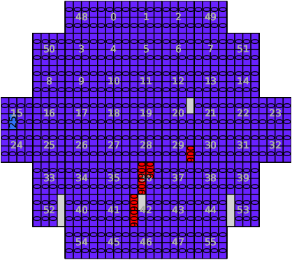
Figure 7a shows the results of a high-level test for all HICANNs of one wafer.
The image shows more test results than the number of dies on the picture of the assembled wafer module.
The reason for this was design constraints and limited routing resources on the Main PCB, by which not all HICANN groups could be electrically connected and thus used within the module context; those at the edge of the wafer were left out.
For the same reason, the two HICANN groups at the center are without high-speed connection.
III-B2 Tests During the Assembly Phase
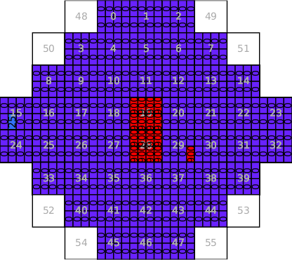
For these additional tests the Main PCB is equipped with test PCBs444Developed by the group of Yasar Gürbüz at Sabanci University, Istanbul, shown in fig. 6c, which measure ESD diode currents and termination resistances between the LVDS lines on the wafer. The tests determine whether a good connection of the wafer to the Main PCB exists. Figure 7b shows the result of one of these tests, where only the same faulty device on HICANN group 29, also detected in the needle card test, can be seen. No additional faulty devices validate that the wafer to Main PCB marriage was appropriate.
III-B3 Post-Assembly Tests of All HICANNs on the Wafer
After the assembly of the wafer module is completed, the same tests run on the pre-assembly phase are conducted, and results are compared. The results for one test are shown in fig. 7c. The errors in HICANN groups and are still present, while the errors in groups and are not. Further investigations could trace these last errors to connection problems of the needle card used in the wafer prober.
IV Commissioning Software
After assembly, additional steps are necessary to bring the BrainScaleS-1 wafer module into readiness for experiments. These include digital tests to find and exclude malfunctioning components and calibrating the individual neurons to address manufacturing-process-induced circuit mismatches. Databases store the results from these two steps, allowing serialized data storage to disk. See [14] for details. Furthermore, all steps are fully automated and periodically executed after installation of the module in the machine room to track the systems’ current state.
IV-A Communication Tests
The first test that is executed on a newly assembled wafer module is the communication test, which is used to find unresponsive HICANNs .
Communication problems most likely arise from insufficient connection quality between the Main PCB and the wafer, cf. [9], or from scratches or similar defects on the post-processing layers.
During the test, an individual connection is established to each of the HICANNs of one wafer.
The test is split into a high-speed test and a JTAG test, which reflects the two possibilities to communicate with the HICANN.
Failures are stored separately in the availability database.
The result of a communication test is shown in fig. 7d.
In this example, the result comparison between the test stand and the rack-mounted fully assembled wafer module shows one additional HICANN group and individual HICANNs that cannot communicate via JTAG .
IV-B Memory Tests
Using a whole uncut wafer, each BrainScaleS-1 wafer module profits from better energy efficiency and higher bandwidth for communication between its ASICs as if these were produced separately and then integrated.
This approach presents a challenge, though, as producing an error-free wafer-scale system in such a way is not possible, as ASICs with manufacturing-induced problems cannot be removed.
The BrainScaleS-1 system addresses this through a digital memory test, which in conjunction with the fault-tolerant system design, enables dynamic handling of malfunctioning components.
Executed after assembly as well as periodically, the test also tracks the state of the systems over time.
Therefore, it allows to operate wafer modules despite a subset of malfunctioning components or connections, consequently increasing the yield of functional systems.
The test builds upon the communication test and establishes a connection to a HICANN group.
First, it initializes the connected communication board and the HICANN under test.
Subsequently, each digital memory is repeatedly write/read-tested using random values.
If a mismatch is found, the largest functional unit that depends on the malfunctioning component is excluded so that it is not utilized in experiments.
HICANNs that can communicate only via JTAG are exclusively used for spike route-through to and from neighboring HICANNs on the same wafer.
For these, a routing-specific reduced memory test minimizes the runtime using the slower connection.
In total, more than of digital memory get tested per wafer.
Results for a fully assembled wafer module are shown in table I.
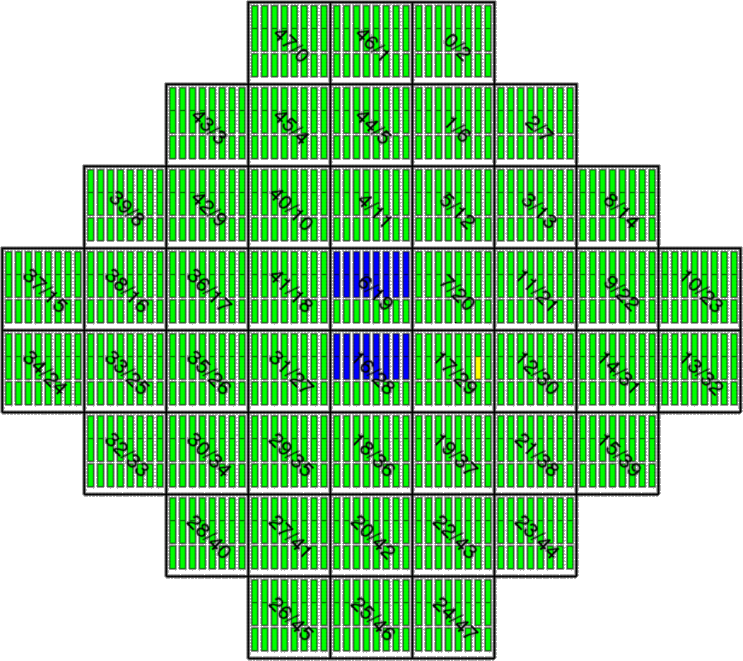
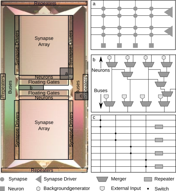
Tested components and their position on the HICANN are visualized in fig. 8.
| Resource | Components | Excluded | |
|---|---|---|---|
| Individual | Effective | ||
| JTAG comm. | 384 | ||
| High-speed comm. | 368/384 | ||
| Synapse drivers | 78320 | ||
| Synapse arrays | 712 | ||
| Synapse rows | 159488 | ||
| Synapses | 40099840 | ||
| FG blocks | 1492 | ||
| External input mergers | 2848/2984 | ||
| Analog outputs | 712 | ||
| Background-generators | 2848 | ||
| Mergers | 5340 | ||
| Buses | -/119360 | - | |
| Repeaters | 119360 | ||
| Switches | 2864640 | ||
With per HICANN , the configuration registers of the synapses make up the largest part of the tested memory.
They are split into two synapse arrays per HICANN , each of which is programmed by a custom on-chip SRAM controller described in [15].
In the tests, on of the synapse arrays, unstable behavior is observed.
This means, consecutive write/read operations with fixed values on a single synapse register show varying results.
Since problems in individual synapse registers are very unlikely and could also derive e.g. from the control chain, a special stability test is introduced.
There, each register is tested several times with the same value.
If a single register shows unstable behavior, the whole synapse array is excluded.
Thereby, at the expense of functional components, only stable programmable synapses are used during experiments.
A test with ten write/reads of random data per component and a stability test with ten repetitions takes approximately per HICANN . Since the tests can be executed in parallel for each HICANN group, a full wafer test takes approximately and can be executed periodically to track the state of the systems.
IV-C Effective Exclusion of Components
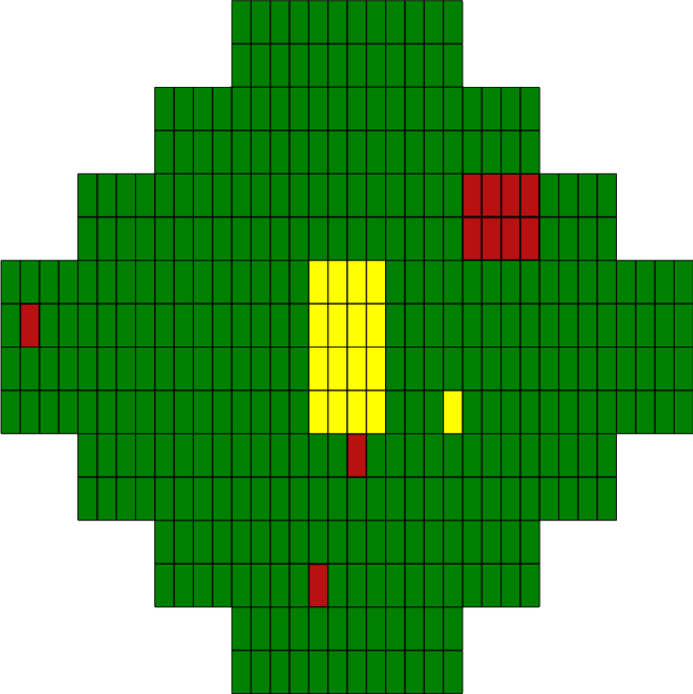
In special cases, it is not enough to skip malfunctioning components during an experiment, but it is also important to be aware of hardware specific dependencies that can be linked with these components. This is achieved through an additional step, the effective exclusion of components, where functional but dependent components are excluded. Several dependencies lead to an effective exclusion. Some of them are visualized in fig. 8.
-
•
Unstable repeater controller: To enhance the signal integrity of spike events that have to be routed across several HICANNs, the signal is regenerated between dies by repeaters. These repeaters are organized in blocks where each block has a custom on-chip controller used to program its repeaters. Since failures in the digital memory of the repeaters are very unlikely, more than one failing repeater per block indicates that there could also be a problem in the control chain. To ensure no unstable components are used, all repeaters connected to the corresponding repeater block are removed from the availability database in such cases.
-
•
Buses connected to malfunctioning repeaters: Buses are used to route spike events between neuron circuits. On boundaries between two HICANNs , the buses are connected to repeaters that regenerate the signal. Each repeater is connected to a bus on its own HICANN as well as on a neighboring one. If a repeater is failing the memory test, there is no possibility to test if it sends wrong signals to its connected buses. To circumvent this, all buses connected to such a repeater are excluded and thus not used during an experiment. The same holds for repeaters on HICANNs without JTAG connection. As the repeaters cannot be initialized correctly, all neighboring buses connected to repeaters on the problematic HICANN are excluded.
-
•
Malfunctioning FG controller: The FGs are not only used to configure the neurons but also to supply bias voltages to the spike event routing. If an error in the controller programming the FGs is found, the whole HICANN is excluded from the availability database and, in the following, treated as if there would be no JTAG connection. Such a HICANN is not used at all in experiments.
-
•
Without high-speed: HICANNs that have no high-speed connection are, due to the higher bandwidth requirements, not used to emulate neurons or external inputs but only used to route spike events. This is achieved by removing all neurons and external input mergers from the availability database.
-
•
No routing options: To improve the placement and prevent lost connections, the algorithm checks that all the components required to establish a route from each neuron and external input merger are available. If not, the neuron or the external input merger is excluded and therefore skipped in the process of building a network.
-
•
Handling hardware versioning: In an earlier version of the post-processing, connections were established to HICANNs on the edges of the wafer that must not be connected. To prevent leakage currents from these dies, the connected buses are excluded. Therefore, it is unnecessary to distinguish wafer versions in all the following steps.
An overview of removed components before and after the effective exclusion of components can be seen in table I. The availability database, used to handle the excluded components, allows for storing different states on disk, so malfunctioning components and effective components can be differentiated afterward. This is for example important during the initialization of the HICANNs, where only malfunctioning components have to be handled specifically.
IV-D Analog Readout Tests
Before usage, the analog recording system gets verified for correct connectivity and configuration by running a series of tests. Each HICANN is set in sequence to generate two different voltage levels, which the AnaRM measures. The voltage levels originate from the configuration of one of the FGs . A recording that agrees with the settings and whose noise levels are within a tolerance threshold indicates that the system is ready for experiments or calibration runs.
IV-E Calibration
VLSI transistors are subject to manufacturing variations translating into differences in signal response. This problem and the potential impacts have been noted since the first approaches to neuromorphic computing using VLSI [16]. Consequently, the HICANN ’s microelectronic analog circuits require correction mechanisms to deliver homogeneous responses.
As the manufacturing variability is stationary within the components’ operating ranges, thus termed fixed-pattern noise, it can be reduced by suitable calibration. To this end, a framework has been developed for the BrainScaleS-1 wafer module that performs a one-time circuit characterization through running sequences of experiments that sweep neuron parameters, measure the effect in the observable, and perform appropriate fits on suitable models. The process creates a database that holds the calibration results and is loaded on routine hardware usage, allowing for automatic translation between biological-space parameters and FG -stored parameters. Such a conversion is automated and transparent for the users when running an experiment. See [14] for details.
The calibration procedure configures all the neuron circuits at once and then processes the individual measurements to allow for programming the FGs in parallel. In addition, parallelizing the analysis algorithms on the already measured steps further optimizes the time required for calibration. Regardless, an increase in the number of calibration steps could improve the quality of the fits, while also parameters that are more sensitive to FG parameter variability benefit from an increase in the number of measurement repetitions. Consequently, calibration time and precision of the results require balancing.
IV-E1 Calibration Methodology
In the BrainScaleS-1 system, the only analog neuron property that can be directly recorded is the membrane voltage. Accordingly, all parameter calibrations are based on membrane recordings under different parameter configurations. In general, the calibration of one parameter sweeps over its operating range while maintaining the rest of the parameters constant. The execution order is relevant, as some calibration routines require an already calibrated subset of parameters. Furthermore, the calibration accounts for analog readout noise, and measurements can be repeated to factor in FG parameter variability.
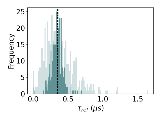
The main neuron calibration parameters are summarized in fig. 9. In the following, the calibration procedure is exemplarily shown for the parameter , which controls the refractory period , i.e., the time after the emission of a neuron’s action potential during which its membrane is clamped to the reset potential and the neuron can elicit no further spike. The higher is, the shorter the achieved . Each calibration step sets the resting potential above the level at which a spike event is elicited, i.e., , which causes the neurons to spike continuously. The inter spike interval (ISI) is the measurable result.
In the first step, is set to maximum, and the corresponding ISI is regarded as ISI 0, the minimum attainable interval under the current settings. Larger refractory periods are referenced to ISI 0 by using
| (1) |
making the minimum zero seconds by definition. Afterward, each step’s distinct target FG values of are programmed, causing changes observable in the ISI and thus in . The obtained set of configured parameters and their achieved refractory periods is then fit to a model, which in the case of corresponds to
| (2) |
Such a model derives from transistor-level simulations described in [17]. The resulting fits for five neurons are shown in fig. 10.
The pair of constants and corresponding to model eq. 2 is stored in the calibration database for each neuron, which is then used for translation from in seconds to in digital value. Further details for each parameter calibration are provided in the supplementary material.
Depending on each parameter’s sensitivity to the programmed FG values, some calibrations enable a more precise setting of parameters than others. An increased sensitivity due to non-linear hardware dependencies is found where small changes in FG values cause large changes in the observables. Furthermore, for some FGs only a limited range of their available parameter space is used, reducing the ability to set their corresponding parameters precisely. As can be seen from the measured values in fig. 10, such is the case for . For comparison, fig. 11 shows how the leak potential , which is easier to control, obtains a more precise calibration than . For this reason, the control precision of several parameters was improved in the second-generation BrainScaleS-2 chip [18] partly by enabling digital value storage.


IV-E2 Synapse Weight Calibration
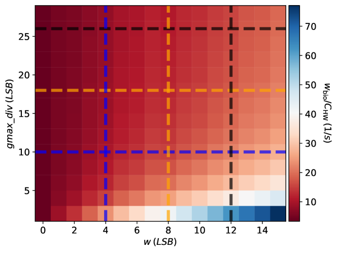
The calibration of the synaptic input differs from the other calibrations due to its additional dependency on the synapse drivers. The strength of a synapse is configured by three hardware parameters. The -bit digital weight stored per synapse, a scaling factor stored per synapse row, and the FG -stored reference parameter . This last parameter is set per synapse row and selects one of four possible values shared by blocks of 128 neurons. Calibrating this large parameter space for each of the neurons with connected synapse drivers using the analog readout system, which allows for measuring membrane traces in parallel, is not possible in a reasonable time frame. Therefore, a per wafer translation is performed, where only some of the components are taken into account to find the average circuit behavior. The measurement requires the results of all previous calibrations. Neurons on different HICANNs are stimulated by a single spike for different combinations of the three hardware parameters to cover the whole parameter range. Subsequently, a fit of the conductance based neuron model is applied to the recorded membrane traces to extract the ratio between biological weight and membrane capacitance . Since the membrane capacitance is fixed during experiments, it is unnecessary to separately determine both values. During the fit, the model parameter of the already calibrated reversal potential is fixed. The reduced value of the fit is used to identify and exclude saturation effects of the involved operational transconductance amplifier (OTA) 1, cf. fig. 9, which might occur for large weight values. Finally, the weight translation is found by fitting the expected hardware behavior
| (3) |
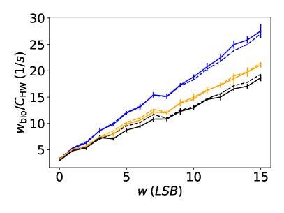
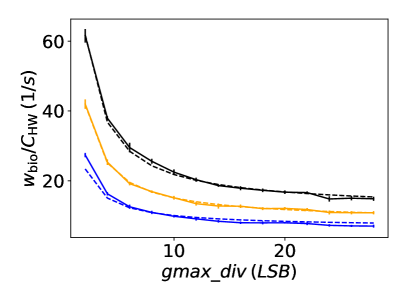
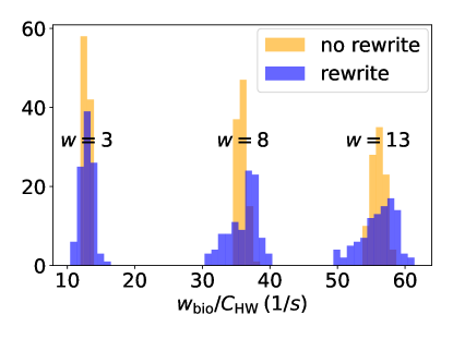
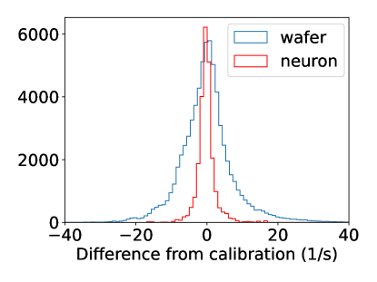
adapted from [19], to the results of the first fits. The fit parameters characterize the effect of parasitic capacitances found in the synaptic circuit for each enabled bit of the -bit weight value . Figure 12a demonstrates the large parameter space of the synapse weight calibration. It shows the measurement of a single neuron, stimulated by a single synapse driver for a single value without rewriting the FGs . The performance of the fit applied on the whole measured parameter space is shown for fixed values of in fig. 12b and for fixed digital weight values in fig. 12c. Although the whole neuron circuit and consequently the expected noise of each individual component is involved, the error of each measurement does not exceed the variations observed in other calibrations. However, additional deviations arise from rewriting the FGs , which is demonstrated in fig. 12d; this renders the search for a more precise fit function unbeneficial. In addition, the per wafer calibration opted over a per neuron circuit calibration introduces a dominant error due to the deviations between neuron circuits, shown in fig. 12e. A precise weight calibration within a reasonable runtime would be achievable via a parallel measurement of each neuron circuit. This would also allow to exclude neurons showing unintended behavior. However, this is not possible with the currently used analog readout system. Nonetheless, the lack of a perfect weight calibration can be circumvented via in-the-loop training on the BrainScaleS-1 system, as shown for inference tasks in previous results [6].
IV-E3 Calibration Based Exclusion of Components
The operation of the HICANNs during the calibration is similar to the operation during experiments. All components have to work correctly for the calibration to succeed. Failing calibrations indicate unintended behavior. This allows for testing the whole die, especially the analog circuits that cannot be tested directly. Additionally, thresholds can be defined to exclude outliers. Consequently, neurons that do not pass all calibration steps are excluded from the availability database. Numbers of calibration based excluded neurons on a typical wafer are given in table II.
| Neurons | Excluded by Calibration | Effective Exclusion |
|---|---|---|
| 182272/190976 |
V Experiment Showcase - Synchronous Firing Chain
Previous experiments on the BrainScaleS-1 system relied on a small subset of the available neurons [6, 20, 21]. In this section, we use a synchronous firing chain (synfire chain) to utilize a large number of the available wafer module resources. We start with a relatively short chain to illustrate the behavior of the network and finally present a longer one that utilizes a large part of a single wafer module.
Synfire chains can filter for synchronous activity and propagate the activity along a chain of neuron groups [22, 23]. We choose synfire chains since they can easily be scaled up to arbitrary sizes by increasing the chain length as well as the number of neurons in a single group and have been studied extensively in previous publications [24, 25, 26]. Furthermore, synfire chains were used to showcase the functionality of the predecessor of BrainScaleS-1 [27] and to characterize the behavior of the current system in software simulations [28].
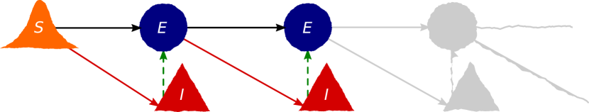
Figure 13 displays a synfire chain with feed-forward inhibition. Each chain link consists of an excitatory and inhibitory population. The inhibitory populations are connected to the excitatory population within the same group. This feed-forward inhibition can enhance the filtering properties of the chain [29, 26]. The excitatory population forwards its outputs to both populations within the next group. External stimulus is injected in the form of Gaussian pulse packages [24]. The strength denotes the number of input spikes per stimulus neuron and the standard deviation of the Gaussian from which the spike times are drawn. We will use to refer to specific packages.
V-A Network Behavior
In a first step we will look at a relatively short chain with six chain links, shown in fig. 14, to illustrate how the filtering properties of the chain can be tuned. Table III summarizes some of the key properties of the network. We used the manual placement described in [14] to place the different populations on the wafer. Specifically, we distribute the external stimulus over several HICANNs in order to minimize spike loss due to limited bandwidth.
| Parameter | Short Chain | Long Chain |
|---|---|---|
| Chain Length | 6 | 190 |
| Stimulus Neurons | 100 | 80 |
| Excitatory Neurons per Group | 100 | 80 |
| Inhihibitory Neurons per Group | 25 | 20 |
| Total Number of Neurons | 750 | 19000 |
| Total Number of Neuron Circuits | 3000 | 76000 |
| Total Number of Synapses | ||
| Used HICANNs | 48 | 230 |
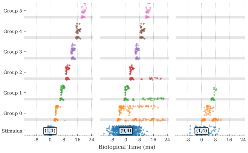
As mentioned previously, synfire chains are able to filter for synchronous input and to synchronize less-synchronous input as it travels along the chain [24, 23]. Figure 14a shows the propagation of three different input stimuli along the chain. In case of a relatively weak and synchronous input a single, narrow package travels along the chain. If the input is stronger and more asynchronous, we observe a broader response in the first groups of the chain which is synchronized as the signal propagates along the chain such that the responses in the final group are comparable. Too weak and asynchronous input, here as an example, dies out and does not cause a response in the final group. This is in agreement with previous results [24, 29, 27, 28].
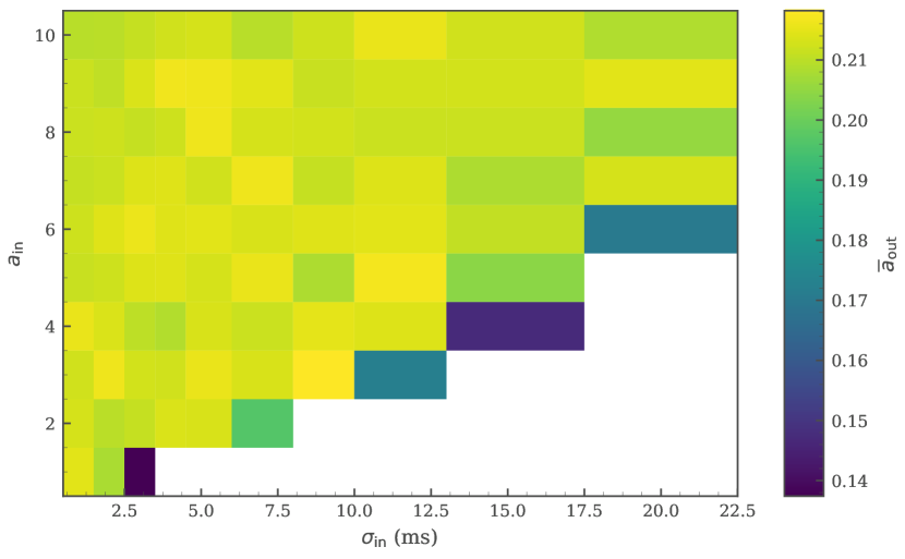
Figure 14b shows in more detail for which input stimuli the propagation along the chain is successful. In agreement with the previous observations, weak and asynchronous input is not transmitted to the final group. The response in the final group is almost uniform. This indicates that the packages are synchronized as they travel along the chain. Setting appropriate parameters which reproduce the expected results from simulations relies on the calibration routines, introduced in section IV-E. The calibration allows to set model parameters in the biological domain and reduces the inherent mismatch between the physical components.
V-B Wafer-Scale Network
The previous section demonstrates the implementation and control of a short synfire chain on the BrainScaleS-1 system. This section shows that the commissioning efforts described in section IV also facilitate the implementation of wafer-scale networks. The properties of this synfire chain are summarized in table III.

The complexity of the emulation increases with the size of the model. While for a relatively short chain it is possible to investigate the behavior of individual neurons and manually detect malfunctioning and bad calibrated entities, this is not feasible for larger experiments. Therefore, digital tests described in section IV-B are essential to automatically avoid these components during the experiment.
To simplify the automatic routing of the abstract network description to physical entities on the wafer, we once again employ manual mapping, see fig. 15a. We place the different groups in a zig-zag pattern starting from the top-left side towards the bottom of the wafer and then back up towards the top-right side. This placement schema allows the BrainScaleS-1 operating system [14] to find appropriate connections between the different populations and minimizes synapse loss, i.e. synaptic connections that could not be mapped to the hardware.
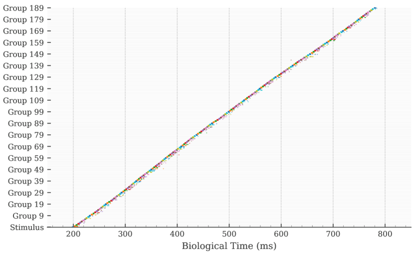
We were able to successfully emulate a synfire chain with chain links on the BrainScaleS-1 system. Figure 15b shows an example of a pulse package that travels along the full length of the chain. The activity of the individual groups still depends on the exact neuron and synapse properties, but the calibration ensures that the pulse package remains compact. A synchronous pulse reaches the final group after a signal propagation time of about in the biological regime, which corresponds to wall-clock time.
VI Discussion
Starting its development more than ten years ago, the first-generation BrainScaleS wafer-scale neuromorphic system represents a milestone toward a large-scale analog neural network emulation platform. Over years during which several modules have been commissioned and experiments run, we have learned important lessons on building and handling such a complex system. We discovered drawbacks in our first implementation; some of them could successfully be circumvented via our commissioning software. Our second-generation neuromorphic BrainScaleS-2 chip [18] addresses BrainScaleS-1’s design weaknesses. Moreover, it enables the application of advanced learning mechanisms by introducing a digital plasticity processor, neuron multi-compartment capabilities, as well as extended analog to digital conversion capacities.
In this paper, we described the individual components of a BrainScaleS-1 wafer module and showed the necessary steps to assemble it. A wafer-scale analog system is complex and requires many hardware components working concurrently. Once a wafer module is assembled, it is often not possible to pinpoint defects in individual components. To alleviate this, each component must get tested on its own; malfunctioning ones must be repaired or replaced before they are added to the system. Additional tests during the assembly are also crucial to allow for finding and solving errors that arise during that process. The remaining problems are handled by the exclusion of affected components or circuits from the availability database to ensure the correct operation of the system.
The importance of the tests and monitoring remains after the wafer module gets placed in the rack. For example, tight monitoring during system operation is necessary to uncover the wear out of system components. Automated alerts are fundamental for warning in case of values deviating over time. Furthermore, the tests executed nightly help keep track of the wafer modules’ state.
Concerning the wafer in the core of the BrainScaleS-1 system, the probability of fabrication defects in microelectronics is proportional to the circuit area [30]. Thus, it is unfeasible to build such a large analog system without malfunctioning components. This will most likely further intensify in the future by utilizing novel materials. With this in mind, the digital tests introduced are executed nightly to identify such malfunctioning components and exclude them from our availability database. These tests enable storing different states of the database on disk and allow to differentiate actual malfunctioning components from those not usable due to a dependency. The users can then utilize reliable components, possibly even using a custom availability database.
An additional challenge using analog hardware is the fixed-pattern noise introduced by unavoidable manufacturing process variations. In the BrainScaleS-1 system, this is worsened by the design decision to use FGs to store the neuron configuration. These cells allow for long-term storage of analog parameters without storing digital values onboard. However, the current implementation introduces write-cycle to write-cycle variability. Though small, these variations lead to noticeable errors if they are further enlarged by non-linear dependencies between control signal and observable. To minimize these effects, we presented our calibration framework, which also allows non-expert users to configure experiments in the biological domain without specific knowledge of the hardware. We demonstrated the narrowing and centering of the achieved value distribution for exemplary parameters after the calibration was applied, limited by thermal noise and the variations caused by the FGs , nonetheless. Since single-poly floating-gate cells are non-standard devices and not supported by the manufacture, the second-generation BrainScaleS-2 chip reverts to a digital parameter storage scheme employed in a previous neuromorphic architecture [31], thereby vastly improving analog parameter accuracy. Since the second generation uses a manufacturing process with much smaller geometry, namely vs. , the area penalty for the digital parameter storage is manageable. A further advantage of the novel parameter storage is the reduced programming time [32]. In the presented wafer-scale implementation, the single-poly floating-gate parameter storage was the only feasible solution to achieve the required number of analog parameters for the neuron circuits.
On top of explaining the calibration methodology, we demonstrated the necessity for parallel execution of the calibrations. The large parameter space of the synapse weight calibration exceeds reasonable runtimes using the current readout system. In order to circumvent this, we introduced a per wafer calibration which, compared to a per circuit calibration, shows larger errors but can be generated in a reasonable time frame. To improve this, we developed a new readout system, which will replace the external set of ADCs with on-wafer-module boards, increasing the parallel readout capabilities from to channels [33]. Moreover, in the BrainScaleS-2 chip, we introduce a per neuron-circuit ADC system, which allows for a massive parallel calibration [18]. A per-circuit calibration before each experiment becomes feasible with such a solution.
Finally, we demonstrated the operation of a fully commissioned BrainScaleS-1 wafer module implementing synfire chains . While small chains portray the capability to fine-tune the network parameters, extending to a long chain of links illustrates the possibility to scale up networks. Successfully mapped to an inherently imperfect substrate, it consists of the largest spiking network emulation run with analog components and individual synapses to date.
Our endeavor in developing and maintaining the BrainScaleS-1 system has demonstrated, while illustrating the field’s challenges, that building wafer-scale analog neuromorphic hardware is feasible. Furthermore, the BrainScaleS-1 wafer module with its operating system laid the foundation for the next-generation systems; all lessons learned from the first generation contribute to the success of future large-scale neuromorphic systems.
Acknowledgments
The authors wish to thank all present and former members of the Electronic Vision(s) research group contributing to the BrainScaleS-1 platform, development and operation methodologies, as well as software development. We thank S. Schiefer and S. Hartmann from the group Hochparallele VLSI-Systeme und Neuromikroelektronik at TU-Dresden for the development and before-assembly routine testing of the communication boards and the WIOs , as well as for providing test details and images for this writing. We thank M. Yaziki and O. Ceylan from the group of Yasar Gürbüz at Sabanci University, Istanbul for the development of test boards that are being used during assembly of the wafer modules. We thank Würth Elektronik, Germany for dedicated and detailed support during the development of the Main PCB. This work has received funding from the EU ([FP7/2007-2013], [H2020/2014-2020]) under grant agreements 604102 (HBP), 269921 (BrainScaleS), 243914 (Brain-i-Nets), 720270 (HBP SGA1), 785907 (HBP SGA2) and 945539 (HBP SGA3), the Deutsche Forschungsgemeinschaft (DFG, German Research Foundation) under Germany’s Excellence Strategy EXC 2181/1-390900948 (the Heidelberg STRUCTURES Excellence Cluster), the Helmholtz Association Initiative and Networking Fund (ACA, Advanced Computing Architectures) under Project SO-092, as well as from the Manfred Stärk Foundation.
References
- [1] D. Brüderle, J. Bill, B. Kaplan, J. Kremkow, K. Meier, E. Müller, and J. Schemmel, “Simulator-like exploration of cortical network architectures with a mixed-signal VLSI system,” in Proceedings of the 2010 IEEE International Symposium on Circuits and Systems (ISCAS). IEEE, May 2010, pp. 2784–2787. [Online]. Available: http://ieeexplore.ieee.org/document/5537005/
- [2] J. Schemmel, J. Fieres, and K. Meier, “Wafer-scale integration of analog neural networks,” in Proceedings of the 2008 International Joint Conference on Neural Networks (IJCNN), 2008.
- [3] J. Fieres, J. Schemmel, and K. Meier, “Realizing biological spiking network models in a configurable wafer-scale hardware system,” in Proceedings of the 2008 International Joint Conference on Neural Networks (IJCNN), 2008.
- [4] J. Schemmel, D. Brüderle, A. Grübl, M. Hock, K. Meier, and S. Millner, “A wafer-scale neuromorphic hardware system for large-scale neural modeling,” in Proceedings of the 2010 IEEE International Symposium on Circuits and Systems (ISCAS), May 2010, pp. 1947–1950. [Online]. Available: http://ieeexplore.ieee.org/document/5536970/
- [5] S. Millner, A. Grübl, K. Meier, J. Schemmel, and M.-O. Schwartz, “A VLSI implementation of the adaptive exponential integrate-and-fire neuron model,” in Advances in Neural Information Processing Systems 23, J. Lafferty, C. K. I. Williams, J. Shawe-Taylor, R. Zemel, and A. Culotta, Eds., 2010, pp. 1642–1650.
- [6] S. Schmitt, J. Klähn, G. Bellec, A. Grübl, M. Güttler, A. Hartel, S. Hartmann, D. Husmann, K. Husmann, S. Jeltsch, M. Kleider, C. Koke, A. Kononov, C. Mauch, E. Müller, P. Müller, J. Partzsch, M. A. Petrovici, B. Vogginger, S. Schiefer, S. Scholze, V. Thanasoulis, J. Schemmel, R. Legenstein, W. Maass, C. Mayr, and K. Meier, “Neuromorphic hardware in the loop: Training a deep spiking network on the BrainScaleS wafer-scale system,” Proceedings of the 2017 IEEE International Joint Conference on Neural Networks (IJCNN), pp. 2227–2234, May 2017. [Online]. Available: http://ieeexplore.ieee.org/document/7966125/
- [7] S. Millner, “Development of a multi-compartment neuron model emulation,” Ph.D. dissertation, Ruprecht-Karls University Heidelberg, November 2012. [Online]. Available: http://www.ub.uni-heidelberg.de/archiv/13979
- [8] T. Lande, H. Ranjbar, M. Ismail, and Y. Berg, “An analog floating-gate memory in a standard digital technology,” in Microelectronics for Neural Networks, 1996., Proceedings of Fifth International Conference on. IEEE Comput. Soc. Press, 12-14 1996, pp. 271 –276. [Online]. Available: http://ieeexplore.ieee.org/document/493802/
- [9] K. Zoschke, M. Guettler, L. Boettcher, A. Gruebl, D. Husmann, J. Schemmel, K. Meier, and O. Ehrmann, “Full wafer redistribution and wafer embedding as key technologies for a multi-scale neuromorphic hardware cluster,” EPTC 2017, 2017.
- [10] L. Sterzenbach, “Entwicklung einer selbstüberwachenden Spannungsversorgung für ein auf Wafer-Ebene integriertes neuromorphes Hardware-System,” Bachelor thesis (German), Hochschule Mannheim University of Applied Sciences, 2014.
- [11] G. Project, “Carbon.” [Online]. Available: https://github.com/graphite-project/carbon
- [12] G. Labs, “Grafana: The open observability platform.” [Online]. Available: https://grafana.com
- [13] elastic, “Elasticsearch: The official distributed search & analytics engine.” [Online]. Available: https://www.elastic.co/elasticsearch
- [14] E. Müller, S. Schmitt, C. Mauch, S. Billaudelle, A. Grübl, M. Güttler, D. Husmann, J. Ilmberger, S. Jeltsch, J. Kaiser, J. Klähn, M. Kleider, C. Koke, J. Montes, P. Müller, J. Partzsch, F. Passenberg, H. Schmidt, B. Vogginger, J. Weidner, C. Mayr, and J. Schemmel, “The operating system of the neuromorphic BrainScaleS-1 system,” Neurocomputing, vol. 501, pp. 790–810, Aug 2022. [Online]. Available: https://linkinghub.elsevier.com/retrieve/pii/S0925231222006646
- [15] S. Friedmann, “A new approach to learning in neuromorphic hardware,” Ph.D. dissertation, Ruprecht-Karls-Universität Heidelberg, 2013.
- [16] C. A. Mead, Analog VLSI and Neural Systems. Reading, MA: Addison Wesley, 1989.
- [17] M.-O. Schwartz, “Reproducing biologically realistic regimes on a highly-accelerated neuromorphic hardware system,” Ph.D. dissertation, Universität Heidelberg, 2013.
- [18] J. Schemmel, S. Billaudelle, P. Dauer, and J. Weis, “Accelerated analog neuromorphic computing,” arXiv preprint, 2020. [Online]. Available: https://arxiv.org/abs/2003.11996
- [19] C. Koke, “Device variability in synapses of neuromorphic circuits,” Ph.D. dissertation, Ruprecht-Karls University Heidelberg, February 2017. [Online]. Available: http://www.ub.uni-heidelberg.de/archiv/22742
- [20] A. F. Kungl, S. Schmitt, J. Klähn, P. Müller, A. Baumbach, D. Dold, A. Kugele, E. Müller, C. Koke, M. Kleider, C. Mauch, O. Breitwieser, L. Leng, N. Gürtler, M. Güttler, D. Husmann, K. Husmann, A. Hartel, V. Karasenko, A. Grübl, J. Schemmel, K. Meier, and M. A. Petrovici, “Accelerated physical emulation of bayesian inference in spiking neural networks,” Frontiers in Neuroscience, vol. 13, p. 1201, Nov 2019. [Online]. Available: https://www.frontiersin.org/article/10.3389/fnins.2019.01201
- [21] J. Göltz, L. Kriener, A. Baumbach, S. Billaudelle, O. Breitwieser, B. Cramer, D. Dold, Á. F. Kungl, W. Senn, J. Schemmel, K. Meier, and M. A. Petrovici, “Fast and energy-efficient neuromorphic deep learning with first-spike times,” Nature Machine Intelligence, vol. 3, no. 9, pp. 823–835, Sep 2021. [Online]. Available: https://www.nature.com/articles/s42256-021-00388-x
- [22] A. Aertsen, M. Diesmann, and M. O. Gewaltig, “Propagation of synchronous spiking activity in feedforward neural networks.” Journal of Physiology-Paris, vol. 90, no. 3-4, pp. 243–247, Jan 1996. [Online]. Available: http://view.ncbi.nlm.nih.gov/pubmed/9116676
- [23] M. O. Gewaltig, M. Diesmann, and A. Aertsen, “Propagation of cortical synfire activity: survival probability in single trials and stability in the mean.” Neural Networks, vol. 14, no. 6-7, pp. 657–673, Jul 2001. [Online]. Available: https://linkinghub.elsevier.com/retrieve/pii/S0893608001000703
- [24] M. Diesmann, M.-O. Gewaltig, and A. Aertsen, “Stable propagation of synchronous spiking in cortical neural networks,” Nature, vol. 402, no. 6761, pp. 529–533, Dec 1999. [Online]. Available: http://www.nature.com/articles/990101
- [25] M. Diesmann, “Conditions for stable propagation of synchronous spiking in cortical neural networks: Single neuron dynamics and network properties,” Ph.D. dissertation, Ruhr-Universität Bochum, 2002.
- [26] A. Kumar, S. Rotter, and A. Aertsen, “Conditions for propagating synchronous spiking and asynchronous firing rates in a cortical network model,” Journal of Neuroscience, vol. 28, no. 20, pp. 5268–5280, May 2008. [Online]. Available: https://www.jneurosci.org/lookup/doi/10.1523/JNEUROSCI.2542-07.2008
- [27] T. Pfeil, A. Grübl, S. Jeltsch, E. Müller, P. Müller, M. A. Petrovici, M. Schmuker, D. Brüderle, J. Schemmel, and K. Meier, “Six networks on a universal neuromorphic computing substrate,” Frontiers in Neuroscience, vol. 7, p. 11, 2013. [Online]. Available: http://www.frontiersin.org/neuromorphic_engineering/10.3389/fnins.2013.00011/abstract
- [28] M. A. Petrovici, B. Vogginger, P. Müller, O. Breitwieser, M. Lundqvist, L. Muller, M. Ehrlich, A. Destexhe, A. Lansner, R. Schüffny, J. Schemmel, and K. Meier, “Characterization and compensation of network-level anomalies in mixed-signal neuromorphic modeling platforms,” PLOS ONE, vol. 9, no. 10, p. e108590, Oct 2014. [Online]. Available: https://dx.plos.org/10.1371/journal.pone.0108590
- [29] J. Kremkow, L. Perrinet, G. Masson, and A. Aertsen, “Functional consequences of correlated excitatory and inhibitory conductances in cortical networks.” Journal of Computational Neuroscience, vol. 28, no. 3, pp. 579–594, Jun 2010. [Online]. Available: http://link.springer.com/10.1007/s10827-010-0240-9
- [30] S. Werner, J. Navaridas, and M. Luján, “A survey on design approaches to circumvent permanent faults in networks-on-chip,” ACM Computing Surveys (CSUR), vol. 48, no. 4, pp. 1–36, May 2016. [Online]. Available: https://dl.acm.org/doi/10.1145/2886781
- [31] J. Schemmel, K. Meier, and E. Muller, “A new VLSI model of neural microcircuits including spike time dependent plasticity,” in Proceedings of the 2004 International Joint Conference on Neural Networks (IJCNN’04). IEEE Press, 2004, pp. 1711–1716.
- [32] M. Hock, A. Hartel, J. Schemmel, and K. Meier, “An analog dynamic memory array for neuromorphic hardware,” in Circuit Theory and Design (ECCTD), 2013 European Conference on, Sep. 2013, pp. 1–4.
- [33] J. Ilmberger, “Development of a digitizer for the brainscales neuromorphic hardware system,” Master thesis, Ruprecht-Karls-Universität Heidelberg, 2017.