Janus monolayer ScXY (XY=Cl, Br and I) for piezoelectric and valleytronic application: a first-principle prediction
Abstract
Coexistence of ferromagnetism, piezoelectricity and valley in two-dimensional (2D) materials is crucial to advance multifunctional electronic technologies. Here, Janus ScXY (XY=Cl, Br and I) monolayers are predicted to be in-plane piezoelectric ferromagnetic (FM) semiconductors with dynamical, mechanical and thermal stabilities. The predicted piezoelectric strain coefficients and (absolute values) are higher than ones of most 2D materials. Moreover, the (absolute value) of ScClI reaches up to 1.14 pm/V, which is highly desirable for ultrathin piezoelectric device application. To obtain spontaneous valley polarization, charge doping are explored to tune the direction of magnetization of ScXY. By appropriate hole doping, their easy magnetization axis can change from in-plane to out-of-plane, resulting in spontaneous valley polarization. Taking ScBrI with 0.20 holes per f.u. as a example, under the action of an in-plane electric field, the hole carriers of K valley turn towards one edge of the sample, which will produce anomalous valley Hall effect (AVHE), and the hole carriers of valley move in a straight line. These findings could pave the way for designing piezoelectric and valleytronic devices.
I Introduction
In two-dimensional (2D) materials, there may be piezoelectric, magnetic or valley properties, and their coupling may provide a potential platform for multifunctional electronic devicesa1 . The combination of piezoelectricity and ferromagnetic (FM) order, namely 2D piezoelectric ferromagnetism (PFM), has been widely investigated by the first-principle calculationsqt1 ; q15 ; q15-0 ; q15-1 ; q15-2 ; q15-3 . Especially, the PFM with large out-of-plane piezoresponse is highly desirable for ultrathin piezoelectric device application. Some of PFMs may have ferrovalley (FV) properties with spontaneous spin and valley polarizationsf10 . In fact, a FV semiconductor with FM ordering must be a PFM due to broken time-reversal and space-inversion symmetries. The piezoelectric properties of some FV semiconductors have been explored theoreticallyf11 ; f12 . The anomalous valley Hall effect (AVHE) driven by piezoelectric effect has been proposed in monolayer f11 . Therefore, searching for 2D PFMs with large vertical piezoelectric response and FV properties is significative and interesting.
2D Janus materials could be potential candidates with out-of-plane piezoelectric response and FV properties due to broken out-of-plane symmetryq16 ; q16-1 , and the representative Janus monolayer MoSSe has been experimentally fabricatede1 ; e2 . The Janus strategy has been used to produce large out-of-plane piezoelectric responseqt1 ; q15 . For example Janus monolayer CrSCl, the predicted out-of-plane piezoelectric strain coefficient is -1.58 pm/Vq15 . Moreover, for many three-layer Janus family, the size of out-of-plane is positively related to electronegativity difference of bottom and top atomsq15 .
Recently, monolayer (X = Cl, Br and I) are predicted to be in-plane FM semiconductors, which are dynamically, mechanically and thermally stable with preserved out-of-plane symmetryf13 . These monolayers provide the foundation for building Janus structures to induce out-of-plane piezoelectric response. In this work, we construct Janus ScXY (XY=Cl, Br and I) monolayers, which are stable in-plane FM semiconductors. Among the three monolayers, due to largest electronegativity difference of Cl and I atoms, ScClI monolayer has the highest (absolute value) of 1.14 pm/V, which is higher than ones (less than 1 pm/V) of most 2D materialsq7 ; q7-2 . After hole doping, the easy magnetization axis changes from in-plane to out-of-plane, and the AVHE can be realized under the action of an in-plane electric field. Taking ScBrI with 0.20 holes per f.u. as a example, the carrier doping density is around 1.53 , which can be realized in Hall devices through available gate techniques. Our works provide potential candidate materials for piezoelectric and valleytronic application.
II Computational detail
Within density functional theory (DFT)1 , we perform the first-principle calculations by using the projector augmented wave (PAW) method as implemented in Vienna ab initio Simulation Package (VASP)pv1 ; pv2 ; pv3 . The generalized gradient approximation of Perdew, Burke and Ernzerhof (GGA-PBE)pbe is adopted as exchange-correlation functional. The on-site Coulomb correlation of Sc-3 electrons is considered by PBE+ method within the rotationally invariant approach proposed by Dudarev et alu , and the 2.5 eVf13 is adopted. The spin-orbital coupling (SOC) is included to investigate magnetocrystalline anisotropy (MCA) energy and valley properties of ScXY (XY=Cl, Br and I). The energy cut-off of 500 eV, total energy convergence criterion of eV and force convergence criteria of less than 0.0001 are set to attain reliable results. A vacuum space of more than 16 between slabs along the direction is added to eliminate the spurious interactions. The phonon spectrum is obtained by using the Phonopy codepv5 with a 551 supercell. The elastic stiffness () are obtained by strain-stress relationship (SSR), and the piezoelectric stress tensors () are calculated by using density functional perturbation theory (DFPT) methodpv6 . The Curie temperature is estimated by Monte Carlo (MC) simulations with a 4040 supercell and loops using Wolff algorithm, as implemented in Mcsolver codemc . A 21211 k-point meshes in the first Brillouin zone (BZ) are used for electronic structures and , and 12211 for FM/antiferromagnetic (AFM) energies and .
| Name | MAE (MSA, MCA) | |||||||||
|---|---|---|---|---|---|---|---|---|---|---|
| 3.649 | 76 | -53 (-3, -50) | 147 | 48.19 | 15.72 | -2.43 | -0.28 | -7.49 | -0.44 | |
| 3.881 | 87 | -228 (-3, -225) | 168 | 41.58 | 12.92 | -2.10 | -0.43 | -7.33 | -0.79 | |
| 3.806 | 77 | -198 (-3, -195) | 149 | 46.48 | 15.13 | -2.32 | -0.70 | -7.39 | -1.14 |
III Main calculated results
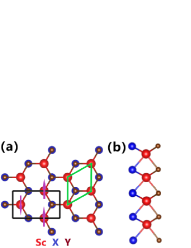
For Janus monolayer ScXY (XY=Cl, Br and I), the crystal structures are shown in Figure 1. The Sc atoms are surrounded by three X and three Y atoms, and form a distorted octahedral structure due to inequivalent Sc-X and Sc-Y bonding lengths caused by different atomic size and electronegativity of X and Y atoms. This also leads to lower space group of (No.156) with respect to monolayer (X=Cl, Br and I)f13 . Therefore, both central inversion symmetry and horizontal mirror symmetry of ScXY are broken, which can induce both in-plane and out-of-plane piezoelectric response. Their energy differences between AFM and FM configurations (=-) are listed in Table 1, and the positive values confirm that they all are FM ground state. The optimized lattice constant with FM ordering are also summarized in Table 1.
The magnetocrystalline direction determines type of magnetic phase transition of 2D hexagonal symmetric system with a typical triangle lattice structure, which can be determined by calculating magnetic anisotropy energy (MAE), including MCA energy () and magnetic shape anisotropy (MSA) energy (). The MCA depends on SOC, and the can be calculated by , where and mean that spins lie in-plane and out-of-plane. The MSA is produced by the anisotropic dipole-dipole (D-D) interactiona1-7 ; a7-1 :
| (1) |
where the represent the local magnetic moments of Sc atoms, and the sites and are connected by vectors . For a collinear FM monolayer, the ()can be written as :
| (2) |
where is the angle between the and . It is clearly seen that the depends the crystal structure and local magnetic moment of magnetic atoms, which tends to make spins be in-plane.
The calculated MAE, MSA and MCA energies of ScXY (XY=Cl, Br and I) are listed in Table 1, and the negative MAE indicate that the three monolayers have an in-plane magnetic anisotropy. It is found that their MSA energies are about -3 with magnetic moment of Sc atom about 0.59 , which is very smaller than MCA energy. Therefore, we will ignore MSA energy in later calculations of MAE. For in-plane case, there is no energetic barrier to the rotation of magnetization in the plane, and a Berezinskii-Kosterlitz-Thouless (BKT) magnetic transition will be produced with a quasi-long-range phasere5 ; re5-1 . Therefore, the ScXY (XY=Cl, Br and I) are 2D magnets. The monte Carlo simulations have shown that BKT magnetic transition takes place at a critical temperature re6 ; re7 , where and are the nearest-neighboring exchange parameter and Boltzmann constant. The can be determined from =-, and the FM and AFM energies with rectangle supercell can be obtained:
| (3) |
| (4) |
where means the total energy of system without magnetic coupling. The corresponding can be expressed:
| (5) |
The predicted of ScXY (XY=Cl, Br and I) (=1) are summarized in Table 1, which are higher than those of experimental discovered 2D ferromagnetic materials (45 K) and (30 K)f3-2 ; f3-3 .
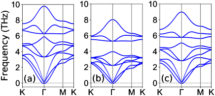
The phonon dispersions of ScXY (XY=Cl, Br and I) are calculated to verify their dynamical stabilities, as shown in Figure 2. All the phonon frequencies are non-negative in the whole BZ, implying that three monolayers are dynamically stable. To further confirm their thermal stabilities, the ab-initio molecular dynamics (AIMD) simulations are performed with a 441 supercell and a time step of 1 fs at 300 K for 8 ps. According to FIG.1 of electronic supplementary information (ESI), the energy of ScXY (XY=Cl, Br and I) fluctuates within a small range during the whole simulation time. Moreover, their snapshots show no structural transitions at the end of the AIMD simulations, manifesting their thermal stabilities. The linear elastic constants of ScXY (XY=Cl, Br and I) are calculated to determine their mechanical stabilities. Due to space group, only two independent elastic constants ( and ) can be observed, which are shown in Table 1. These and meet Born-Huang criteria of mechanical stability ( and )ela , thereby verifying their mechanical stabilities.
Due to unique Janus structure of ScXY (XY=Cl, Br and I), the broken central inversion symmetry and horizontal mirror symmetry can induce both in-plane and out-of-plane piezoelectric response. By using Voigt notation, due to space group, the 2D elastic tensor, piezoelectric stress and strain tensors can be reduced intoq7 ; q7-2 :
| (6) |
| (7) |
| (8) |
With an imposed uniaxial in-plane strain, /0 and /0. However, /=0, but /0, when a biaxial in-plane strain is applied. Here, the two independent and can be derived by :
| (9) |
A piezoelectric material should be a semiconductor to prevent leakage current. The energy band structures of ScXY (XY=Cl, Br and I) with intrinsic in-plane magnetization are calculated, as shown in FIG.2 of ESI. It is clearly seen that they all are indirect bandgap semiconductors. The conduction band bottom (CBM) of three monolayers all are at M point, and the valence band maximum (VBM) locates at point except for ScBrI at K/-K point. The orthorhombic supercell (see Figure 1) is used to calculate the / of ScXY (XY=Cl, Br and I). The elastic constants (, , - and +) and piezoelectric stress coefficients ( and ) along the ionic and electronic contributions of ScXY (XY=Cl, Br and I) are shown in FIG.3 of ESI. For of three monolayers, the electronic and ionic parts have superposed contributions, and the ionic part is larger than electronic one. However, the electronic and ionic contributions of have opposite signs, and the electronic part dominates the piezoelectricity.
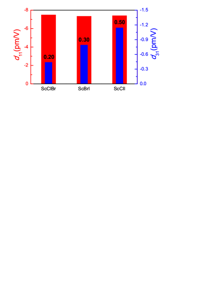
And then, their / of ScXY can be calculated from Equation 9, which are plotted in Figure 3 along with the electronegativity difference between X and Y atoms. It is found that the of three monolayers are almost the same (absolute value for about 7.40 pm/V), which is higher than ones of many 2D materialsq7 ; q7-2 . A large out-of-plane piezoelectric response (for example high ) is highly desired to be compatible with the nowadays bottom/top gate technologies to meet the needs of practical application,. For many 2D Janus families, the size of out-of-plane response is positively related to electronegativity difference of bottom and top atomsq15 . It is clearly seen that ScXY family is also accord with this law. From ScClBr to ScBrI to ScClI, the electronegativity difference of X and Y increases, and then the enhances. For ScClI, the (absolute value) reaches up to 1.14 pm/V, which is higher ones of most 2D materials (1 pm/V), such as oxygen functionalized MXenes (0.40-0.78 pm/V)q9 , Janus TMD monolayers (0.03 pm/V)q7 , functionalized h-BN (0.13 pm/V)o1 , kalium decorated graphene (0.3 pm/V)o2 , Janus group-III materials (0.46 pm/V)q7-6-1 , Janus BiTeI/SbTeI monolayer (0.37-0.66 pm/V)o3 , - (0.415 pm/V)o4 and MoSO (0.7 pm/V)re-11 . The large out-of-plane piezoelectric response also has been predicted in some 2D materials, such as NiClI (1.89 pm/V)qt1 , TePtS/TePtSe (2.4-2.9 pm/V)re-6 , CrSCl (1.58 pm/V)q15 and (1.138 pm/V)q15-1 . However, the ScClI possesses FM ordering with large in-plane piezoelectric response with respect to these 2D materials.
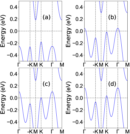
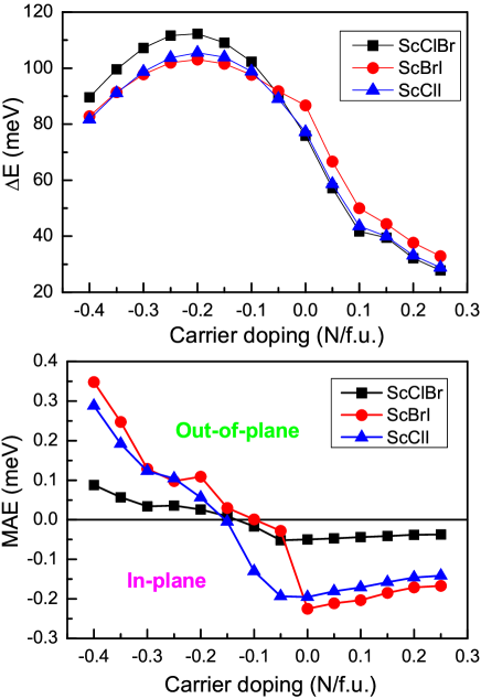
According to the Sc- band structure projection of ScXY (FIG.2 of ESI), the -K and K valleys of valence band are near the Fermi level with / characters. This means that the spontaneous valley polarization will be produced, when the magnetization direction is tuned to out-of-plane case by external field, such as magnetic field, electric field and carrier dopingf13 ; f16 ; f17 . Here, the carrier doping with the concentration of -0.40.25 carriers per f.u. is used to tune magnetization direction of ScXY, and the negative/positive values mean the hole/electron doping. For ScXY (XY=Cl, Br and I), the energy differences between AFM and FM orderings and MAE as a function of carrier doping concentration are plotted in Figure 4. It is found that the FM ordering is always ground state in considered doping range for three monolayers, and the FM interaction can be enhanced in a certain hole doping range. In considered doping range, the MAE of SxXY is always negative for the electron doping, indicating that their magnetization direction is always in-plane. Fortunately, the easy axis becomes out-of-plane, when the hole doping concentration is beyond about 0.15/0.10/0.15 holes per f.u. for ScClBr/ScBrI/ScClI.
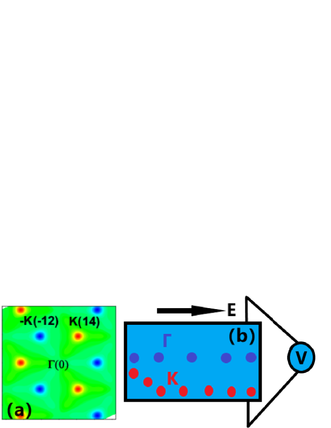
The energy band structures of monolayer ScBrI with representative hole doping are plotted in Figure 5, and those of ScClBr and ScClI are shown in FIG.4 and FIG.5 of ESI. For undoped ScBrI monolayer, the energy at K point is higher than one at point. The hole doping make the energy at point become higher than one at K point. When the hole doping concentration is over 0.15 holes per f.u, the K valley is also doped. For undoped case, the Berry curvature distribution of ScBrI with assumed out-of-plane direction is plotted in Figure 6. The Berry curvature mainly occurs around -K and K valleys with opposite signs and unequal magnitudes, and Berry curvature around valley is almost zero. Under an in-plane longitudinal electric field , the carriers with the nonzero Berry curvature can obtain the general group velocity and anomalous transverse velocity xd ; qqq :
| (10) |
where is along the electric field direction, and is perpendicular to the electric field and out-of-plane directions. For ScBrI with 0.20 holes per f.u., under an in-plane longitudinal electric field , the hole carriers of K valley turn towards one edge of the sample due to anomalous transverse velocity , which will induce a charge Hall current with a voltage (namely AVHE), and the hole carriers of valley move in a straight line (see Figure 6). The corresponding carrier doping density is around 1.53 , which can be experimentally realized by available gate techniques.
The Curie temperature of ScBrI with 0.20 holes per f.u. is estimated with the spin Hamiltonian under the Heisenberg model:
| (11) |
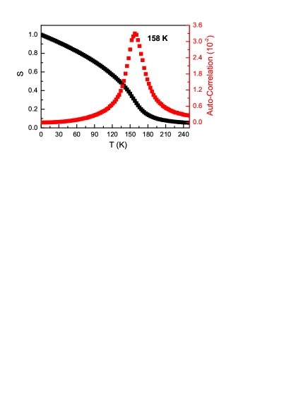
where , and are the nearest exchange parameter, spin quantum number and MAE, respectively. The can be calculated by Equation 5, and the corresponding value is 12.88 meV. The magnetic moment and auto-correlation as a function of temperature are plotted in Figure 7, and the is predicted to be about 158 K, which is higher than those of 2D ferromagnetic materials (45 K) and (30 K)f3-2 ; f3-3 .
IV Conclusion
In conclusion, the piezoelectric and valley
properties of Janus ScXY (XY=Cl, Br and I) are systematically studied by first-principles calculations.
Calculated results show that these monolayers are in-plane FM semiconductors with excellent stability.
The findings indicate that the piezoelectric and FM properties can be combined in monolayer ScXY (XY=Cl, Br and I), and both in-plane and out-of-plane piezoelectric coefficients are higher than those of most known 2D materials.
Under appropriate holes doping, the easy magnetization axis of these monolayers turns to out-of-plane from in-plane, and the AVHE can be realized under the action of an in-plane electric field. Our works provide a development guide for searching 2D multifunctional materials.
SUPPLEMENTARY MATERIAL
See the supplementary material for AIMD results, projected energy band structures and elastic/piezoelectric stress coefficients of ScXY (XY=Cl, Br and I), and the energy band structures of ScClBr and ScClI with hole doping.
Conflicts of interest
There are no conflicts to declare.
Acknowledgements.
This work was supported by Natural Science Basis Research Plan in Shaanxi Province of China (No. 2021JM-456). We are grateful to Shanxi Supercomputing Center of China, and the calculations were performed on TianHe-2.References
- (1) P. Lin, C. Pan and Z. L. Wang, Mater. Today Nano 4, 17 (2018).
- (2) S. D. Guo, Y. T. Zhu, K. Qin and Y. S. Ang, Appl. Phys. Lett. 120, 232403 (2022).
- (3) S. D. Guo, X. S. Guo, Y. T. Zhu and Y. S. Ang, Appl. Phys. Lett. 121, 062403 (2022).
- (4) G. Song, C. F. Zhang, Z. Z. Zhang, G. N. Li, Z. W. Li, J. Du, B. W. Zhang, X. K. Huang and B. L. Gao, Phys. Chem. Chem. Phys.24, 1091 (2022).
- (5) S. D. Guo, X. S. Guo, X. X. Cai, W. Q. Mu and W. C. Ren, J. Appl. Phys. 129, 214301 (2021).
- (6) G. Song, D. S. Li, H. F. Zhou et al., Appl. Phys. Lett. 118, 123102 (2021).
- (7) J. H. Yang, A. P. Wang, S. Z. Zhang, J. Liu, Z. C. Zhong and L. Chen, Phys. Chem. Chem. Phys., 21, 132 (2019).
- (8) W. Y. Tong, S. J. Gong, X. Wan, and C. G. Duan, Nat. Commun. 7, 13612 (2016).
- (9) S. D. Guo, J. X. Zhu, W. Q. Mu and B. G. Liu, Phys. Rev. B 104, 224428 (2021).
- (10) Y. F. Zhao, Y. H. Shen, H. Hu, W. Y. Tong and C. G. Duan, Phys. Rev. B 103, 115124 (2021).
- (11) M. Yagmurcukardes, Y. Qin, S. Ozen, M. Sayyad, F. M. Peeters, S. Tongay and H. Sahin, Appl. Phys. Rev. 7, 011311 (2020).
- (12) L. Zhang, Z. J. F. Yang, T. Gong et al., J. Mater. Chem. A 8, 8813 (2020).
- (13) A.-Y. Lu, H. Zhu, J. Xiao, C.-P. Chuu, Y. Han, M.-H. Chiu, C.-C. Cheng, C.-W. Yang, K.-H. Wei, Y. Yang, Y. Wang, D. Sokaras, D. Nordlund, P. Yang, D. A. Muller, M.-Y. Chou, X. Zhang and L.-J. Li, Nat. Nanotechnol. 12, 744 (2017).
- (14) J. Zhang, S. Jia, I. Kholmanov, L. Dong, D. Er, W. Chen, H. Guo, Z. Jin, V. B. Shenoy, L. Shi and J. Lou, ACS Nano 11, 8192 (2017).
- (15) Y. Z. Wu, J. W. Tong, L. Deng, F. F. Luo, F. B. Tian, G. W. Qin and X. M. Zhang, Acta Mater. 246, 118731 (2023).
- (16) L. Dong, J. Lou and V. B. Shenoy, ACS Nano, 11, 8242 (2017).
- (17) M. N. Blonsky, H. L. Zhuang, A. K. Singh and R. G. Hennig, ACS Nano 9, 9885 (2015).
- (18) P. Hohenberg and W. Kohn, Phys. Rev. 136, B864 (1964); W. Kohn and L. J. Sham, Phys. Rev. 140, A1133 (1965).
- (19) G. Kresse, J. Non-Cryst. Solids 193, 222 (1995).
- (20) G. Kresse and J. Furthmller, Comput. Mater. Sci. 6, 15 (1996).
- (21) G. Kresse and D. Joubert, Phys. Rev. B 59, 1758 (1999).
- (22) J. P. Perdew, K. Burke and M. Ernzerhof, Phys. Rev. Lett. 77, 3865 (1996).
- (23) S. L. Dudarev, G. A. Botton, S. Y. Savrasov, C. J. Humphreys and A. P. Sutton, Phys. Rev. B 57, 1505 (1998).
- (24) A. Togo, F. Oba, and I. Tanaka, Phys. Rev. B 78, 134106 (2008).
- (25) X. Wu, D. Vanderbilt and D. R. Hamann, Phys. Rev. B 72, 035105 (2005).
- (26) L. Liu, X. Ren, J. H. Xie, B. Cheng, W. K. Liu, T. Y. An, H. W. Qin and J. F. Hu, Appl. Surf. Sci. 480, 300 (2019).
- (27) X. B. Lu, R. X. Fei, L. H. Zhu and L. Yang, Nat. Commun. 11, 4724 (2020).
- (28) K. Yang, G. Y. Wang, L. Liu , D. Lu and H. Wu, Phys. Rev. B 104, 144416 (2021).
- (29) K. Sheng, Q. Chen , H. K. Yuan and Z. Y. Wang, Phys. Rev. B 105, 075304 (2022).
- (30) J. L. Lado and J. Fernndez-Rossier, 2D Mater. 4, 035002 (2017).
- (31) P. Jiang, L. Kang, Y.-L. Li, X. Zheng, Z. Zeng, and S. Sanvito, Phys. Rev. B 104, 035430 (2021).
- (32) S. Zhang, R. Xu, W. Duan, and X. Zou, Adv. Funct. Mater. 29, 1808380 (2019).
- (33) C. Gong, L. Li, Z. Li, H. Ji, A. Stern, Y. Xia, T. Cao et al., Nature 546, 265 (2017).
- (34) B. Huang, G. Clark, E. Navarro-Moratalla, D. R. Klein, R. Cheng, K. L. Seyler, D. Zhong et al., Nature 546, 270 (2017).
- (35) R. C. Andrew, R. E. Mapasha, A. M. Ukpong and N. Chetty, Phys. Rev. B 85, 125428 (2012).
- (36) J. Tan, Y. H. Wang, Z. T. Wang, X. J. He, Y. L. Liu, B. Wanga, M. I. Katsnelson and S. J. Yuan, Nano Energy 65, 104058 (2019).
- (37) A. A. M. Noor, H. J. Kim and Y. H. Shin, Phys. Chem. Chem. Phys. 16, 6575 (2014).
- (38) M. T. Ong and E. J. Reed, ACS Nano 6, 1387 (2012).
- (39) Y. Guo, S. Zhou, Y. Z. Bai, and J. J. Zhao, Appl. Phys. Lett. 110, 163102 (2017).
- (40) S. D. Guo, X. S. Guo, Z. Y. Liu and Y. N. Quan, J. Appl. Phys. 127, 064302 (2020).
- (41) L. Hu and X. R. Huang, RSC Adv. 7, 55034 (2017).
- (42) M. Yagmurcukardes and F. M. Peeters, Phys. Rev. B 101, 155205 (2020).
- (43) Z. Kahraman, A. Kandemir, M. Yagmurcukardes and H. Sahin, J. Phys. Chem. C 123, 4549 (2019).
- (44) H. X. Cheng, J. Zhou, W. Ji, Y. N. Zhang and Y. P. Feng, Phys. Rev. B 103, 125121 (2021).
- (45) S. D. Guo, X. S. Guo, G. Z. Wang, K. Cheng and Y. S. Ang, J. Mater. Chem. C 10, 16363 (2022).
- (46) X. Xu, W. Yao, D. Xiao and T. F. Heinz, Nat. Phys. 10, 343 (2014).
- (47) D. Xiao, M. C. Chang, and Q. Niu, Rev. Mod. Phys. 82, 1959 (2010).