Hot-electron resonant terahertz bolometric detection in the graphene/black-AsP field-effect transistors with a floating gate
Abstract
We evaluate the terahertz (THz) detectors based on field effect transistor (FET) with the graphene channel GC and a floating metal gate (MG) separated from the GC by a black-phosphorus (b-P) or black-arsenic (b-As) barrier layer (BL). The operation of these GC-FETs is associated with the heating of the two- dimensional electron gas in the GC by impinging THz radiation leading to thermionic emission of the hot electrons from the GC to the MG. This results in the variation of the floating gate potential, which affects the source-drain current. At the THz radiation frequencies close to the plasmonic resonance frequencies in the gated GC, the variation of the source-drain current and, hence, the detector responsivity can be resonantly large.
I Introduction
The specific properties of graphene channel (GCs) [2, 3, 4] and black-P (b-P), black-As (b-As) , or black-AsP (b-AsP) layers [5, 6, 7, 8, 9] open up prospects for devices based on the GCs (see, for example, the review [10]) and
on the GC/b-AsP heterostructures [7], including the electron devices using
the real-space transfer over the b-AsP layers [11, 12]
and different optoelectronic devices [13, 14, 15, 16].
Due to relatively low energy barriers for the electrons and holes at
the GC/b-AsP interface,
the thermionic emission through such an interface can be effective, particularly,
enabling the creation of the GC/b-AsP- bolometric terahertz (THz) detectors.
In this paper, we evaluate the characteristics of the bolometric detectors
based on the field-effect transistor (FET) structures with the GC, b-AsP
barrier layer (BL), and floating metal gate (MG).
Similar GC/b-AsP FET detectors were recently proposed and analyzed by us [17].
The principal difference between the GC/b-AsP FETs considered previously and
the GC/b-AsP FETs under consideration here is the floating MG.
The idea of using MG in graphene bolometers has been applied to pyroelectric graphene mid-infrared
detectors. In these detectors, pyroelectric substrate charge is collected by a floating gate [18].
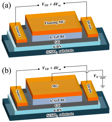
In contrast, the operation of the bolometric detectors considered in this paper is associated with the thermionic emission of the electrons heated by the impinging THz radiation from the GC into the MG via the b-AsP BL. However, contrary to the devices studied in [17], in which the gate current serves as the detected signal, in the detector with the floating MG considered here the detected signal is associated with the variations of the source-drain current in the GC stimulated by the varying potential of the MG. The potential of the latter is controlled by the thermionic emission from the GC, which reinforces with increasing THz power. This effect can become rather strong at the plasmonic oscillations resonantly excited by the impinging THz radiation in the gated GC [19, 20, 21, 22, 23]. The features of the GC-FET detector operation with the floating gate require the development of a fairly different device model. Using this model, we calculate the signal current and the detector responsivity as functions of the structural parameters. As demonstrated, the floating gate GC/b-AsP FET detectors might exhibit elevated values of the responsivity, particularly, at the plasmonic resonances. We also compare the performance of GC/b-AsP FET detectors with the floating and biased MGs.
II Electron transport
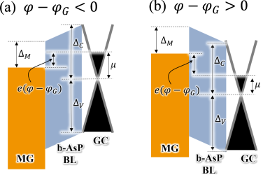
We consider the GC/b-AsP FETs with the floating MG and the b-AsP gate BL. Figures 1 and 2 schematically show the cross-section of the device structures and their band diagrams. The bias voltage and the signal voltage are applied between the FET source and drain as shown in Fig. 1(a). The signal voltage is produced by an antenna receiving the impinging THz radiation with the frequency . The GC of the FETs is doped by donors. For definiteness, the work functions of the gate metal and the b-AsP BL, and the GC doping level (the electron Fermi energy in the GC in equilibrium when no bias is applied) are chosen to provide the band alignment in the equilibrium. This corresponds to , where and are the differences between the work functions of the gate metal and the b-AsP BL and between the b-AsP BL and the GC.
At the source-drain bias voltage and the THz irradiation, the source-drain current, , and the electron effective temperature, , in the GC averaged over the THz radiation period can be presented as
| (1) |
Here and , is the source-drain current at the 2DEG effective temperature equal to the lattice , and are the pertinent current and temperature variations, and and are the variations caused by the source-drain bias voltage and the signal voltage .
The source-drain current per unit of the GC width is governed by the following equations:
| (2) |
where is the density of the thermionic current between the GC and the MG, and is the electron Drude conductivity in equilibrium with being the characteristic electron scattering frequency in the GC (the inverse electron momentum relaxation time), and is the electron Fermi energy, which generally differs from due to the MG charging.
The averaged GC potential (dependent on the coordinate directed along the GC) satisfies the following conditions at the source and drain contacts:
| (3) |
where is the spacing between the contacts (the GC length). Considering the difference between the GC potential and the MG potential and accounting for the quantum capacitance [24, 25] of the gated GC, at not too-large potential swing we obtain
| (4) |
Here , , is the BL dielectric constant, and cm/s is the electron velocity in GCs. This implies that an increase in leads to an increase in the 2DEG density and, hence, its Fermi energy . The contribution of the quantum capacitance to Eq. (4) is characterized by a factor .
Since the MG is disconnected (floating MG),
| (5) |
Due to the trapezoid shape of the barrier between the GC and the MG, the potential barrier heights for the electron emitted from the GC and the MG, and , are equal to:
and for , and
and for .
In this situation, the density of the thermionic current, , between the GC and the MG is given by
| (6) |
when , and
| (7) |
when . Here is the maximum current density, is the electron density in the G-channel, and is the characteristic try-to-escape time from the G-channel. From Eqs. (2), (4), (6), and (7), we obtain
| (8) |
when , and
| (9) |
when .
Here
| (10) |
Setting, for example, meV, meV, ps-1, ps, m, , nm, and meV, we obtain and [ meV].
At low or moderate bias source-drain voltages and THz radiation powers, and are small. In this case, linearizing Eqs. (8) and (9), we arrive at
| (11) |
Equation (11) corresponds to the thermionic current density
| (12) |
Using Eq. (11) with Eq. (3) and taking into account the smallness of parameter [i.e., neglecting the term in the right-hand side of Eq. (11)], for the source-drain current with the pertinent accuracy we obtain
| (13) |
Using Eqs. (5) and (12), we find the MG potential:
| (14) |
The latter equation corresponds to an increase in the source-drain current with increasing gate potential (due to an increase in the Fermi energy and, hence, the G-channel conductivity). One can see that an increase in the 2DEG effective temperature leads to the intensification of the electron transfer from the G-channel to the gate which results in its lower potential.
Equations (13) and (14) for the source-drain current components yield
| (15) |
and
| (16) |
with and and being the effective temperature average of the THz period and the GC length and the GC width, respectively. The quantity given by Eq. (16) represents the response of the GC-FET to the impinging THz radiation.
| Structure | (meV) | (meV) | (meV) | (m) | (THz) | (ps-1) | (m) | (V/W) | |
|---|---|---|---|---|---|---|---|---|---|
| GC/b-P/Al | 85 | 225 | 140 | 1.0 | 1.136 | 1.0 - 2.5 | 1.02 | 1.58 - 1.00 | |
| GC/b-As/Ti | 70 | 190 | 120 | 1.0 | 1.052 | 1.0 -2.5 | 1.29 | 0.93 - 0.59 |
III Electron heating and heat transport
The electron heat transport equation can be presented as
| (17) |
For the variation of the 2DEG averaged effective temperature , in view of Eqs. (5) and (12), Eq. (17) yields
| (18) |
Here is the electron thermal conductivity (per electron), is the electron energy relaxation time, Re is the real part of the 2DEG ac conductivity, and is the signal electric fields in the G-channel created due to the THz signals. The first, second, and third terms in the left-hand side of Eq. (18) are associated with the removal of the electron heat through the contact (due to a substantial electron lateral heat conductivity along the GC [26, 27]), the transfer to the lattice (primarily due to the interaction with optical phonons in the GC and the interface optical phonons [28, 29, 30, 31, 32]) and the MG over the BL (i.e., corresponding to the Peltier cooling [33, 34]), respectively. The term on the right-hand side of Eq. (13) corresponds to the 2DEG Joule heating.
We use the following boundary conditions for Eq. (18):
| (19) |
For the THz radiation asymmetric input via the antenna corresponding to the signal potential at the contacts equal to , accounting for the excitation of plasmonic oscillations in the GC we obtain
| (20) |
Here and are the effective wavenumber and the plasmonic frequency, respectively, with and being the dielectric constant of the BL and its thickness,
Restricting our consideration by the most interesting case of the pronounced fundamental plasmonic resonance in the G-channel () and using Eq (15), we obtain
| (21) |
One needs to note that the Joule power at the plasmonic resonance given by Eq. (21) exceeds that at low frequencies (at least near ) by a factor .
Solving Eq. (18) accounting for boundary condition (19) and Eq. (21), for the values at the fundamental plasmonic resonance we obtain
| (22) |
Here
| (23) |
is the factor characterizing the role of electron thermal transport. and
The characteristic length is the electron heat transfer (cooling) length.
Equations (16) and (22) yield
| (24) |
The sign ”minus” in Eq. (24) reflects the fact that the THz irradiation leads to an increase in the electron effective temperature, reinforcement of the electron emission from the GC and, hence, to a negative charging of the MG. The latter, in turn, decreases the source-drain current in the donor-doped GC.
IV Detector responsivity
Considering that for the half-wavelength dipole antenna with the gain one obtains , where is the THz power at the frequency collected by the detector antenna and is the speed of light in vacuum, and accounting for that the GC channel resistance is equal to , for the detector voltage responsivity (at the radiation frequency corresponding to the fundamental plasmonic resonance), we obtain
| (25) |
Here .
The quantities , , and , are determined by the material of the MG and the molar fractions of As in the BL (due to the condition assumed in our model).
Examples of the parameters of the GC-FET detectors based on Al/b-P/GC and Ti/b-As/GC heterostructures (see, for example, Refs. [34] and [35]) and the estimates of their resonant responsivity are listed in Table I. We assume also that , ps, ps, nm, meV ( K), and V. The above parameters (with ps-1 and or with ps-1 and ) correspond to the GC-FET detector resistances and , respectively (at ). One needs to note that at the above parameters the electron thermal transport factor depending on the ratio in Eq. (23) is rather small (about 0.061 – 0.151 at ps-1) substantially decreasing the responsivity. The role of the electron cooling due to the thermal transport to the side contacts can be decreased by increasing (this decreases the electron thermal conductivity) or choosing the longer GC length .
Figure 3 shows the responsivity of the GC/b-AsP and GC/b-As FETs with a floating MG at (i.e., at the fundamental plasmonic resonance) calculated for the main parameters corresponding to Table I but for different electron scattering frequencies . For the definiteness, we set V. The inset in Fig. 3 shows how the role of the electron thermal transport along the GC changes with varying scattering frequencies. The pertinent dependence is associated with the vs dependence. As follows from Fig. 3, an increase in (i.e., a weakening of the electron heat transfer to the source and drain contacts when becomes larger) leads to slowing of the vs dependence. Thus, a relatively weak dependence of on is interpreted by the decrease in the electron system Joule heating in the GC by the signal electric field (because of ) accompanied with a decrease in the power transferred to the source and drain contacts.
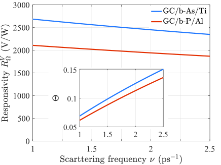
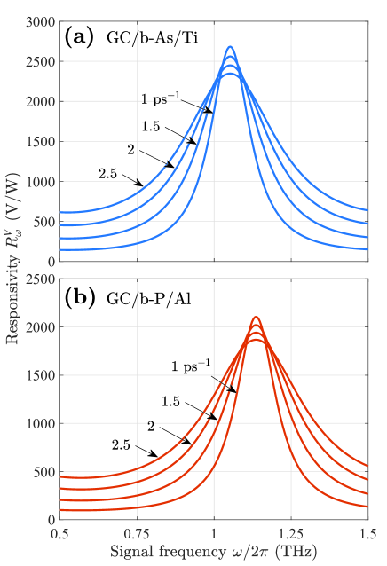
Figure 4 shows the spectral dependences of the responsivity, , of the GC/b-As and GC/b-P detectors calculated for different and the same parameters as for Fig. 3. We limited our consideration by the signal frequencies around the fundamental plasmonic resonance, where the obtained dependences exhibit pronounced maxima provided that . As seen from Fig. 4, an increase in gives rise to a smearing of the resonant peak. In a wider frequency range, the responsivity of the detectors under consideration is a profoundly oscillatory function of the radiation signal frequency with a set of the maxima at the plasmonic resonances ( is the resonance index). These oscillations are described by the relation, which follows from the above equations:
| (26) |
As follows from Eq. (26), the dependences vs exhibit the alternation of sharp maxima and relatively deep minima. At the intermediate frequencies, the responsivity at the minima, is smaller than the resonant responsivity by a factor of . At elevated collision frequencies , the spectral characteristics of become smoother. However, up to (this corresponds to ps-1, at the plasmonic resonances and between the resonances the responsivity can be still relatively high. Hence, the non-resonant response can also be useful.
V Comments
Above we assumed that . Theoretical studies show that the doped GC() conductivity can exhibit different dependences on [37, 38, 39]. In particular, it can vary from virtually independent of if the short-range scattering of electrons is dominant to in the case of the long-range scattering (for example, on charged clusters) [39]. In the first situation , where is the electron momentum. In the second case, . In this regard, our model corresponds to an intermediate vs relation (see, for example, Ref. 37), in which the momentum dependence of is disregarded. This provides ( is the voltage swing between the GC and the gate). The latter qualitatively agrees with the experimental data [2]. In such a case, setting constant (see, for example,Ref. 38), we obtain the relation
| (27) |
which was used above.
Considering that the resonant voltage responsivity, , of GC/b-AsP FETs with the biased gate can be estimated as [17]
| (28) |
for the ratio of the voltage responsivities we obtain
| (29) |
For the typical parameters used above and mV, the latter ratio is about unity, although it increases with further (linearly) increase in . The latter might be limited by the lattice heat removal via the substrate and the contacts. Setting ps-1, for the thermal power we obtain mW at V and mW at V.
As follows from the obtained results, both the current and voltage responsivities are proportional to the source-drain bias voltage . The dark current is also proportional to . This implies that the noise-equivalent power (NEP) and the dark current-limited detectivity of the detectors under consideration vary with increasing source-drain voltage as NEP and , respectively.
For the GC/b-As and GC/b-P detectors with the above parameters at V, we obtain NEP pW/Hz1/2 and NEP pW/Hz1/2 (for the GC/b-As and GC/b-P FETs, respectively), which appears to be promising (compare with other THz bolometers [10]). If m, the latter corresponds to cm Hz1/2/W cm Hz1/2/W, which is about of or exceeding the detectivity of other uncooled THz bolometers (see, for example, Ref. 39). However, one needs to note that NEP increases and decreases with increasing .
Since the operation speed of the detectors under consideration is determined by the characteristic times of the electron cooling, , associated with the energy relaxation on phonons and the heat transfer over the BL, and the gate recharging time. The latter is estimated as . The comparison of these characteristic times yields
| (30) |
For the device structural parameters assumed above , we obtain . This implies that the GC/b-AsP FET bolometers response time is about ps.
The values of the collision frequencies used in the above calculations can be expressed via the electron mobility . Using the relation , where is the so-called fictitious electron mass in GCs, for meV and ps-1, we obtain the range cm/Vs (compare, for example, with Refs. 40, and 41). According to the estimates [42], the room temperature mobility in the GCs on h-BN at the electron density corresponding to the above the Fermi energy can be about cm/Vs. The latter corresponds to ps-1. The quality of the interface between the GC (placed atop of h-BN) and the b-P BL can limit the values of and . The pertinent room temperature electron mobility obtained experimentally several years ago is equal to cm/Vs [43] ( exceeds cm/Vs at K). This corresponds to not too small . One can expect that the contemporary technology is able to provide the GC/b-P interface with sufficiently small , at which the parameter (, so that the plasmonic resonances are pronounced. A substantial reinforcement of the plasmonic resonances in the GC-FET detectors can be realized in the case of the composite gate BL, which includes a relatively narrow b-P BL (and the MG) and the h-BN (or WSe2 [44]) sections between the b-P section and the source in drain. In such a GC-FET detector, the sharpness of the plasmonic resonances might be determined by the GC main part (encapsulated by h-BN and providing small electron collision frequency), by the thermionic current flows via the narrow b-P window.
Similar THz detection properties can be expected in the GC/b-AsP FET devices with the floating isolated doped graphene gate (GG). The main distinction between the detectors with the MG and the detectors with the GG is the different plasmonic response in the latter because of the GG influence on the plasmonic oscillations in the double-graphene structures [45, 46, 47]. Another option is to use the MG consisting of an array of metallic islands (MIs) or quantum dots (QDs). In such a case, each MI/QD has its own floating potential determined by the electron exchange between the MG/QD and the GC (compare with the devices analyzed in Ref. 9). Due to this, the potential distribution along the GC and the effect of the floating MG on the source-drain current can be markedly different from that considered above. However, the consideration of the detectors in question requires a proper modification of the device model and, therefore, a separate treatment.
VI Conclusions
We estimated the room temperature characteristics of the proposed GC/b-AsP FETs with the floating MG operating in the THz frequency range at room temperature. We showed that these detectors can exhibit high values of responsivity at the plasmonic resonances ( V/W) and rather short response times ( ps).
Author contributions
All authors contributed equally to this work.
Acknowledgments
The Japan Society for Promotion of Science (KAKENHI Grants 21H04546 and 20K20349), Japan; RIEC Nation-Wide Collaborative Research Project R04/A10; the US Office of Scientific, Research Contract N00001435, (Project Monitor Dr. Ken Goretta).
Conflict of Interest
The authors declare no conflict of interest
Data availability
All data that support the findings of this study are available within the article.
References
- [1]