Performance in beam tests of Carbon-enriched irradiated Low Gain Avalanche Detectors for the ATLAS High Granularity Timing Detector
Abstract
The High Granularity Timing Detector (HGTD) will be installed in the ATLAS experiment to mitigate pile-up effects during the High Luminosity (HL) phase of the Large Hadron Collider (LHC) at CERN. Low Gain Avalanche Detectors (LGADs) will provide high-precision measurements of the time of arrival of particles at the HGTD, improving the particle-vertex assignment. To cope with the high-radiation environment, LGADs have been optimized by adding carbon in the gain layer, thus reducing the acceptor removal rate after irradiation. Performances of several carbon-enriched LGAD sensors from different vendors, and irradiated with high fluences of 1.5 and neq/cm2, have been measured in beam test campaigns during the years 2021 and 2022 at CERN SPS and DESY. This paper presents the results obtained with data recorded by an oscilloscope synchronized with a beam telescope which provides particle position information within a resolution of a few m. Collected charge, time resolution and hit efficiency measurements are presented. In addition, the efficiency uniformity is also studied as a function of the position of the incident particle inside the sensor pad.
1 Introduction
The High Granularity Timing Detector (HGTD) [1, 2] will be added to the ATLAS experiment [3] during the so-called Phase-II upgrade preceding the high-luminosity phase of the LHC (HL-LHC) [4, 5]. Low Gain Avalanche Detector (LGAD) sensors [6] have been extensively studied during the R&D phase of the HGTD project. These sensors must meet performance targets regarding time resolution of () per hit, collected charge and hit efficiencies of 97% (95%) at the start (end) of their lifetime. The expected maximum fluence is neq/cm2 [2]. These requirements should be achieved taking into account a discriminator of about of the front-end ASIC foreseen for HGTD, ALTIROC [7].
Many previous beam test campaigns were devoted to quantifying LGAD performances before [8, 9] and after [10, 11] irradiation. A variety of pad structures, such as single-pad diodes and segmented arrays of pad diodes with various granularities, from several vendors were tested to prove they meet the requirements to be operated over the entire HL-LHC lifetime. Irradiated devices met the required performance up to neq/cm2, however, some optimization was still required.
In beam tests [11] as well as in laboratory measurements [12], it was observed that the addition of carbon in the gain layer helps reducing the operating voltage needed to collect the same charge by a reduction of the acceptor removal rate after irradiation, hence improving the radiation hardness [13] of the sensors. This is extremely important at higher fluences where standard LGADs need a rather high voltage to maintain their performance (gain, time resolution) after irradiations.
Beam test campaigns conducted in the last three years have been devoted to study the performances of LGAD sensors from different vendors and irradiated with higher fluences, neq/cm2. Some of these beam tests were also used to analyze the sensor mortality rates when exposed to high-intensity beams to mimic end-of-life conditions of HGTD LGADs at the HL-LHC. A second paper is under preparation and will describe this particular phenomenon.
The present paper aims to describe the performance of a selection of promising LGAD sensors with carbon enriched gain layer that could equip the future HGTD. The tested LGADs are described in Section 2. The response of the LGADs to particles has been tested in test beam facilities with an experimental set-up presented in Section 3. The collected data are analyzed according to the method described in Section 4. The results of these tests are presented in Section 5.
2 Sensors
The prototypes tested in this paper were manufactured by Fondazione Bruno Kessler (FBK) in Povo, Italy and by the Institute of Microelectronics (IME) of the Chinese Academy of Sciences in China, where the latter are of two different designs, one by the Institute of High Energy Physics (IHEP) and the other by the University of Science and Technology of China (USTC), both in China. An additional device produced by Centro National de Microelectrónica (CNM) Barcelona, Spain is included in the tests for timing purposes due to its excellent time resolution before irradiation. However, its full performance is not described in this paper as it was studied in the past [8].
In order to study the LGAD performance after irradiation, the sensors were exposed to fluences up to 2.51015 neq/cm2 at the TRIGA reactor in Ljubljana, Slovenia with fast neutrons. Table 1 lists the LGAD sensors measured in the beam tests, including the vendor, the sensor IDs, the implant of the multiplication layer as well as the irradiation type and fluence. It also includes the device name assigned to each sensor for easier reference in the text: a concatenation of the sensor vendor (CNM, FBK, USTC, IHEP) and the irradiation level in units of 1015 neq/cm2. For instance, CNM-0 refers to an unirradiated CNM LGAD, which was used in all beam tests as a time reference.
| Device name | Vendor | Sensor ID | Implant | Irradiation type |
|
Tested at | ||
| CNM-0 | CNM | W9LGA35 | boron | unirradiated | – | DESY/CERN | ||
| FBK-1.5 | FBK | UFSD3.2 W19 | boron + carbon | neutrons | 1.51015 | DESY/CERN | ||
| FBK-2.5 | FBK | UFSD3.2 W19 | boron + carbon | neutrons | 2.51015 | DESY/CERN | ||
| USTC-1.5 | USTC-IME | v2.1 W17 | boron + carbon | neutrons | 1.51015 | DESY | ||
| USTC-2.5 | USTC-IME | v2.1 W17 | boron + carbon | neutrons | 2.51015 | DESY | ||
| IHEP-1.5 | IHEP-IME | v2 W7 Q2 | boron + carbon | neutrons | 1.51015 | DESY/CERN | ||
| IHEP-2.5 | IHEP-IME | v2 W7 Q2 | boron + carbon | neutrons | 2.51015 | CERN |
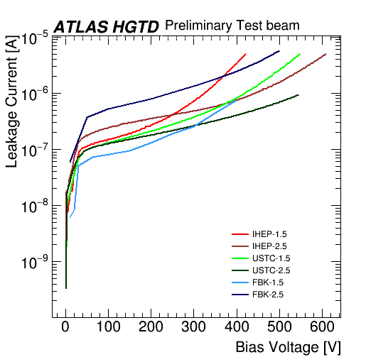
Figure 1 shows the leakage current-voltage (I-V) characteristics for several tested sensors. The I-V measurements for all sensors revealed a leakage current below at about .
2.1 FBK devices
These samples are LGAD sensors optimized for timing, also known as Ultra-Fast Silicon Detectors (UFSDs) [14, 15, 16] which combine an optimized sensor geometry with a moderate internal gain to achieve a time resolution of for minimum ionizing particles (MIPs).
This production run is called UFSD3.2 and aimed to investigate different gain layer designs where two different gain depths were considered: shallow and deep. The gain layer depth is and the active thickness in most of the wafers is . In particular, with respect to the previous production run UFSD3, this one has an optimization of the carbon level and a different array inter-pad gap. Devices in W19 have a thinner bulk for a better time resolution and a combination of deep gain layer and carbon implantation. Different boron doses are considered: 0.70, 0.74, 0.78 (W19), 0.94 and 0.98 (W7) in arbitrary units (a.u.). as well as carbon doses: 0.4, 0.6 (W19), 0.8 and 1 (W7) in a.u. Different diffusion cycles are used, in particular, low (W7) and high (W19) implantation energies. The units could not be made available due to non-disclosure agreement and are not the same for all the producers mentioned in this paper.
The combination of deep gain layer, high doping and carbon implantation shows exceptional performance for the devices from wafer W19 compared with those from wafer W7 (shallow gain layer, carbon, same type as FBK old production UFSD3, active thickness). W19 shows improved behavior: lower voltage for a similar collected charge, better time resolution and lower power dissipation. The carbon dose for devices in W19 is 0.6 a.u. The acceptor removal mechanism reduces the effective doping concentration in the gain layer and the sensor performance can be partially recovered by increasing the applied bias voltage after irradiation. The gain layer depletion voltage, Vgl, varies with the fluence as given by:
| (2.1) |
where c is the acceptor removal coefficient. For these devices (W19), this coefficient is cm2 [17].
2.2 IHEP-IME devices
The production run for the IHEP-IME devices considered in this paper is called version 2 [18], yielding silicon wafers with a -thick high-resistivity epitaxial layer, from which 3 out of 8 are carbonated. The wafers were split into four quadrants. The implantation and diffusion scheme is carbon implantation and diffusion plus boron implantation and diffusion (CHBL) for wafers W7 and W8, and CLBL for wafer W4. The carbon doses differed from quadrant to quadrant in the wafer and the values that were considered in the full production are 0.2, 0.5, 1, 3, 5, 6, 8, 10 and 20 a.u. The most promising devices belong to wafer W7 and quadrant Q2 with a carbon dose of 0.5 a.u. The acceptor removal coefficient for these devices (W7Q2) is 1.1410-16 cm2. The breakdown voltage, Vbd, is around . Before irradiation Vgl is .
2.3 USTC-IME devices
The production run for the USTC-IME devices considered in this paper is called version 2.1 [19], yielding 8-inch wafers with a epitaxial layer from which 4 out of 5 are carbonated. The gain layer dose is medium and the energy is low. The implantation is boron and the carbon dose is 1 a.u. The wafers include small arrays. The average breakdown voltage is about , the Vbd is in the range of . An under bump metallization was deposited on the wafers and afterwards were diced. This version aimed to lower the Vbd to enhance the irradiation hardness further and improve and evaluate the yield of the 1515 arrays. Devices from wafer W17 show impressive radiation hardness. The acceptor removal coefficient for these devices (W17) is about 1.23 cm2.
Table 2 summarizes the different properties of the tested sensors in terms of Vgl0, diffusion scheme and acceptor removal coefficient.
| Device name | Vgl0 [V] | Diffusion | c [cm2] |
|---|---|---|---|
| FBK-1.5/2.5 | 50 | H | |
| USTC-1.5/2.5 | 27 | L | |
| IHEP-1.5/2.5 | 25 | CHBL |
3 Test beam set-up
One HGTD beam test campaign was conducted at DESY [20] on beamline 24 using a electron beam followed by a campaign at the CERN SPS [21] H6A line using a high-momentum pion beam. The beam profile size was about cm2 in both cases. The set-up used at DESY was identical to the set-up described in detail in [11].
The LGADs were mounted on custom readout boards [22] with on-board and external amplification stages to enhance their signal. The position of the devices under test (DUTs) was coherently controlled by a micrometric motor stage in the plane perpendicular to the beam axis ( direction).
The set-up included a beam telescope in which six planes were used to track the incident charged particles. The telescope’s role was to provide the position of the incoming particles in the frame of each DUT to perform efficiency measurements. A four-channel oscilloscope was used to sample the waveforms from the DUTs. A trigger system was used to initiate the data acquisition (DAQ) of the oscilloscope and the tracking planes, which can be uniquely linked by a common event number. The trigger fired on a signal from the tracking system, except during oscilloscope dead time or times during which the telescope or reference tracking plane was in a “busy” state.
3.1 Set-up at DESY
The time resolution of each DUT was estimated by testing it with two other devices, including a time reference system. At DESY, a silicon photomultiplier (SiPM) combined with a quartz bar provided a time reference that was acquired by the DAQ together with two DUTs. The measured time resolution from this device was found to be 62.60.6 ps for an operating voltage of . This time resolution was degraded compared to the previous measurements [11] due to ageing and irradiation effects.
The set-up included a EUDET telescope based on six MIMOSA [23] pixel planes. It was combined with an FE-I4 [24] readout chip-based module to reconstruct the tracks. A plastic scintillator coupled to a photomultiplier tube was also used in the front of the set-up. The coincidence between the FE-I4 hitOR signal and the scintillator signal was used to trigger the data-taking. The FE-I4 chip was configured to consider only signals in a region of interest (ROI) compatible with the DUT geometries. The trigger logic was handled by a programmable Trigger Logic Unit (TLU) [25]. Moreover, a NIM logic circuit was implemented to generate a busy signal covering the time the oscilloscope needed to read out its data buffer. Dry ice-based cooling was used to maintain, but not control, the temperature of the DUTs between to . The monitoring of the temperature and humidity was performed with Pt100 probes.
3.2 Set-up at CERN
The set-up at CERN relied on the MALTA telescope [26]. MALTA is a full-scale monolithic pixel detector implemented in TowerJazz CMOS technology. It contains a small pixel electrode that allows for the implementation of a fast, low-noise and low-power front-end, which is sensitive to the charge released by ionising radiation in a 20–25 m deeply depleted region. The novel asynchronous matrix architecture is designed to ensure low power consumption and high rate capability.
The MALTA telescope installed in the North Area of CERN, on the H6 beamline, consists of six MALTA chips, three on each side of the DUT. The timing reference is a second LGAD sensor, CNM-0, which has been placed next to the cooling box. It has been calibrated in the lab and in beam tests to a time resolution of 54.8 ps at room temperature. Its time resolution at a temperature of is . For triggering on a particle, the second MALTA sensor is used in coincidence with a scintillator placed at the back of the telescope. If the two sensors record a signal, an FPGA-based triggering system records the telescope data from all six planes and the waveforms from both the DUT and the LGAD used as a timing reference. A remote-controlled cooling system was used to maintain the temperature of the DUTs at in a hermetic box.
4 Data analysis
Two independent systems were used to collect the data processed in this analysis: the oscilloscope, which provides data on the LGAD and SiPM waveforms, and the telescope (MALTA at CERN and EUDET-type at DESY) which gives information on the particle tracks.
This section describes the general methodology used to reconstruct and process the information from these two chains, and how it is used to derive the physical quantities for the analysis.
4.1 Track reconstruction for data taken during DESY beam tests with EUDET-type telescope
The EUDET-type telescope and FE-I4 together provided tracking information allowing the reconstruction of the trajectory of particles and the identification of the specific position where the DUT was hit.
The tracking capability of the EUDET-type telescope was provided by six MIMOSA planes as explained in section 3.1. The positions of the MIMOSA, FE-I4 and DUT planes were recorded with a precision of in the -direction along the beam line. The positions of the hits from each MIMOSA plane, together with their respective -coordinate, were used to reconstruct particle trajectories and the (,)-coordinates of hits in the DUT planes.
After the removal of so-called “hot” pixels from the MIMOSA planes, identified as those with an occupancy higher than ten times the average, the remaining hits were grouped into clusters. Only clusters with a maximum of 20 hits were used for tracking. The cluster coordinates were the centroid of the hit coordinates in and . Only events with exactly one cluster in the FE-I4 were considered. The MIMOSA planes were aligned by iteratively shifting the planes’ coordinates in and direction with respect to a reference plane. This procedure aimed to minimize the difference between the reconstructed track position at the MIMOSA plane and the measured hit position in the same plane. The position resolution was taken as the resolution of the fit performed during the alignment procedure.
Given the -position of the MIMOSA planes along the beam axis and the - and -positions of the hits in these planes, three-dimensional (3D) tracks were built. The procedure is described in [8] and [11] for data taken during beam tests at CERN SPS with 120 GeV pion beam for which tracks are straightforward, as multiple scattering can be considered negligible. For data collected at DESY with a 5 GeV electron beam, the procedure was slightly different because electrons may be scattered in the equipment around the DUTs. As shown in figure 2, 3D-proto-tracks are reconstructed from the three MIMOSA planes before the DUTs on the beam trajectory (“upstream triplets”), and other 3D-proto-tracks are reconstructed from the three MIMOSA planes after the DUTs (“downstream triplets”). The downstream triplets must coincide with a hit in the FE-I4 plane.
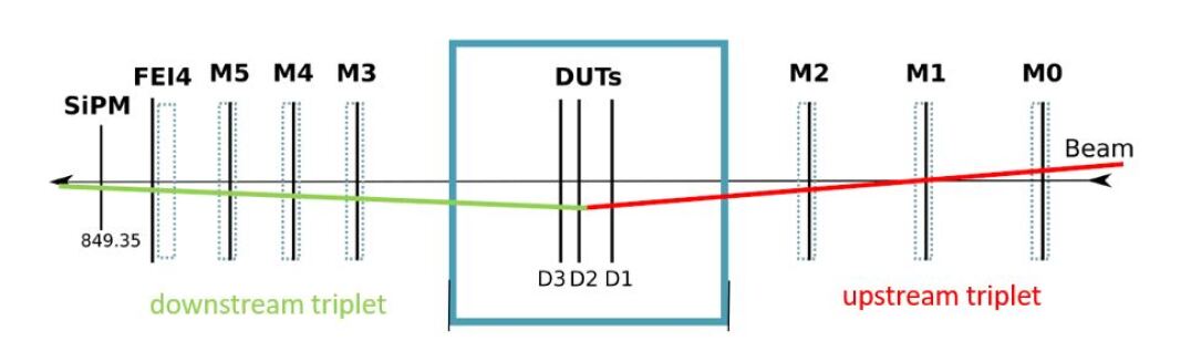
For each event, all possible downstream and upstream triplets are reconstructed and a complete track is considered to be found if a downstream triplet matches an upstream triplet in the central region with a minimal distance of approach of 150 m. Only events with a single complete track through the six MIMOSA planes are considered.
4.2 Track reconstruction for data taken during CERN SPS beam tests with MALTA telescope
The event reconstruction, including coarse alignment, fine alignment and tracking, was done using the software package Proteus [27]. Adjacent pixel hits were combined into clusters. The tracks reconstructed from these three telescope layers was extrapolated to the plane of the DUT, taking into account multiple scattering using the General Broken Lines (GBL) formalism. The precision of the positional resolution using six MALTA chips is less than .
4.3 Oscilloscope data processing
A complete description of the LGAD waveform processing can be found in [11]. In summary, the procedure is the following: after the start and stop points of the pulse were determined, the pedestal was computed in a region outside the pulse where no signal was expected. This pedestal was subtracted from all the data points of the waveform on an event-by-event basis. After that subtraction, the start and stop points were re-computed. Several waveform properties can be extracted at this step such as the maximum of the pulse amplitude, the charge, the rise time, the jitter, the signal-to-noise ratio and the time of arrival (TOA).
The maximum of the pulse amplitude was estimated as the sample with the maximum amplitude. The collected charge was defined as the integral of the pulse in the signal region divided by the trans-impedance of the read-out board and the gain of the voltage amplifier. The TOA was calculated with a constant fraction discriminator (CFD) method and it was defined as the point at which the signal crosses a predefined fraction () of its total amplitude. For the analysis of the DESY beam test data, the TOA value at was used for the SiPM whereas for the DUTs, the TOA value was chosen to be .
The last step was to produce a merged file containing the oscilloscope and telescope data together. In this way, for each event and for each DUT, both the information extracted from the oscilloscope waveforms and the position of the hit of the beam particle in the sensor plane are available for a common analysis.
5 Sensors performance results
The studies presented in this paper aim to evaluate the performance of carbon-enriched LGAD sensors at two irradiation levels, 1.5 and 2.51015 neq/cm2, with particle beams using the reconstructed position of the tracks in the sensor planes. The following LGAD properties have been investigated: the collected charge, the time resolution and the hit reconstruction efficiency.
5.1 Data selection
In all subsequent analyses, background events were removed with a timing cut using a window from the maximum point of the distribution of the difference between the TOA of the DUT and that of the SiPM. Additionally, the signal amplitude in the SiPM was required to be three times higher than the noise level.
The value of the discriminator of the future ALTIROC chip corresponds to a collected charge of , as explained in section 1. The efficiency and the time resolution were computed using this threshold in the analysis.
To measure the global efficiency and the collected charge of the sensors, another condition was added: only the fiducial region of 0.5x0.5 mm2 in the center of the DUTs was used.
5.2 Collected charge
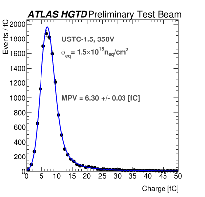
After the background removal, for each DUT, the distribution of the charge (defined in section 4.3) was fitted with a Landau-Gaussian convoluted function. The collected charge reported for each sensor was defined as the most probable value (MPV) from this fit. Figure 3 shows an example distribution for sensor USTC-1.5.
Figures 4 and 5 show the collected charge as a function of bias voltage for different single-pad sensors irradiated at fluences of neq/cm2 and neq/cm2, respectively. Bias voltages were kept lower than the single event burnout (SEB) voltage at which the sensor dies due to a large amount of energy deposited by a highly energetic particle in the active zone [28]. All sensors characteristics are given in section 2. In both figures, the results come either from sensors tested at DESY with electrons or from sensors tested at CERN with pions. The methods to analyse these two types of data from different tracking devices are described in sections 4.1 and 4.2.
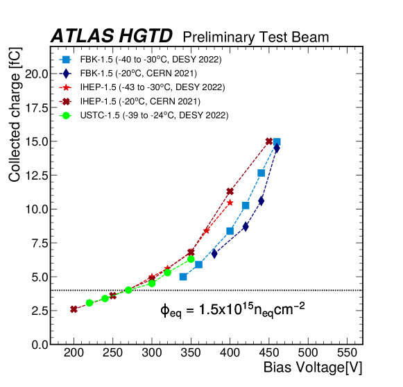
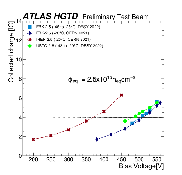
Figure 4 shows that after an irradiation at a fluence of neq/cm2, the collected charge is above the minimum required charge of needed for a good timing measurement with the future HGTD detector. This minimum is reached at around for all sensors, however the sensor FBK-1.5 was tested at higher bias voltages. For sensor IHEP-1.5, the same performances were found whether measurements were performed with a electron beam at DESY or with a pion beam at CERN. For sensor FBK-1.5, at the same bias voltage, the collected charge was slightly higher for measurements at DESY than for those at CERN. Between and , which is the range with common bias voltage, the sensors manufactured by IHEP and USTC showed better performances than those from FBK.
The comparison between figures 4 and 5 shows that the higher the fluence, the worse the collected charge at the same bias voltage. Indeed, figure 5 shows that after an irradiation at a fluence of neq/cm2, the minimum required collected charge of is reached for a bias voltage around for sensor IHEP-2.5, around for sensor FBK-1.5 and for sensor USTC-2.5. Comparing the different sensors at this fluence, those manufactured by IHEP show better performance than sensors from FBK and USTC at the same bias voltage. This discrepancy is less significant at a fluence of neq/cm2.
5.3 Time resolution
The time resolution is one of the key parameters when assessing LGAD sensor performance and has been explained in detail in [11]. To extract the DUTs’ time resolutions, the distributions of the difference between the TOA of the DUTs and that of the time reference device (SiPM at DESY and CNM-0 at CERN) was used.
During the DESY beam test campaign, there were two DUTs (labelled as and in equation 5.1) and one SiPM connected to the oscilloscope. Hence, it was possible to compute three time differences on an event-by-event basis between all these devices:
| (5.1) |
The three distributions were fitted with a gaussian function, each of them giving a width where and are the names of the devices used for each distribution. Assuming that the time resolution of the devices are independent, each of measured resolution corresponds to
| (5.2) |
where and are the resolutions of each device. This gives a system of three equations and three unknowns which can be solved analytically.
No matter which DUTs are tested, the SiPM time resolution should have the same value. Overall, during the DESY beam test campaign, the SiPM time resolution was measured 17 times with this method and its average resolution was found to be ps with variations up to 7 % due to differences in running conditions (e.g. bias voltage settings).
During the CERN beam test campaign, the time reference was given by CNM-0 with a known time resolution of 54.8 ps. The time resolution of the DUT was computed as for the DESY analysis: the distribution of the difference between the TOAs of the reference LGAD and the DUT was fitted with a gaussian function, giving a width . The time resolution of the DUT is then directly given by the equation:
| (5.3) |
where ps.
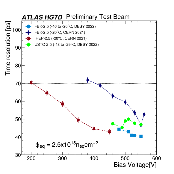
Figures 6 and 7 show the time resolution as function of the bias voltage for different single-pad sensors irradiated at fluences of neq/cm2 and neq/cm2 respectively. In both figures, the results come either from sensors tested at DESY with electrons or from sensors tested at CERN with pions.
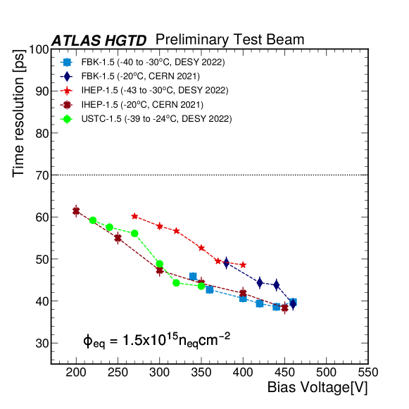
Both figures show an improvement in the time resolution with higher bias voltage, as expected. Figure 6 shows that sensors irradiated at a fluence of neq/cm2 can achieve a time resolution of around for sensors FBK-1.5 and IHEP-1.5 at a bias voltage of 450 V and of for sensor USTC-1.5 at a bias voltage of 350 V.
Figure 7 shows that even after an irradiation at a fluence of neq/cm2, time resolution measurements can almost reach the same values as after an irradiation at a lower fluence of neq/cm2. Indeed, at a higher bias voltage of , sensors FBK-2.5 and USTC-2.5 can achieve a time resolution of and of , respectively. Sensor IHEP-2.5 achieves a time resolution of around at the same bias voltage of 450V as for the measurement at a fluence of neq/cm2.
5.4 Hit reconstruction efficiency
The hit reconstruction efficiency is defined as the number of reconstructed tracks giving a signal on the center of the sensor for which the charge in the sensor is greater than a given threshold value, Qcut, divided by the total number of reconstructed tracks crossing the same fiducial region:
| (5.4) |
As explained in the paragraph 5.1, Qcut is set to .
5.4.1 Efficiency as a function of the bias voltage
Figures 8 and 9 show the efficiency as a function of bias voltage for different single-pad sensors irradiated at fluences of neq/cm2 and neq/cm2, respectively. In both figures, the results come either from sensors tested at DESY with electrons or from sensors tested at CERN with pions.
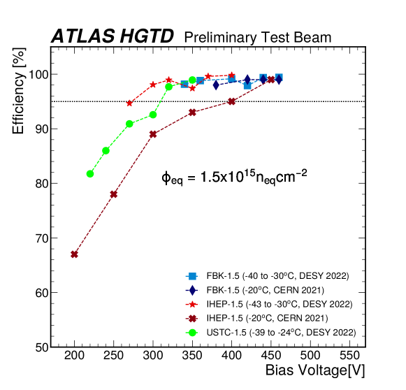
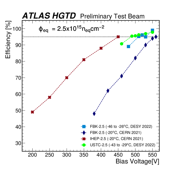
Both figures show that a higher efficiency can be reached by increasing the bias voltage. Figure 8 shows that all DUTs irradiated at a fluence of neq/cm2 can achieve an efficiency of more than 98.9%. Figure 9 shows that at a higher fluence of neq/cm2, the bias voltage needs to be higher than at neq/cm2 to reach almost similar performances or just below. Indeed, at a fluence of neq/cm2, the sensors tested at DESY reach an efficiency of 99% for FBK-2.5 and 98.1% for USTC-2.5. This is well beyond the efficiency of 95% required for good operation of the future HGTD after irradiation. As for the time resolution, the effects of the temperature can also be seen in the efficiency: the sensors tested at CERN at a higher temperature of reach a lower efficiency of 95%.
5.4.2 Efficiency uniformity
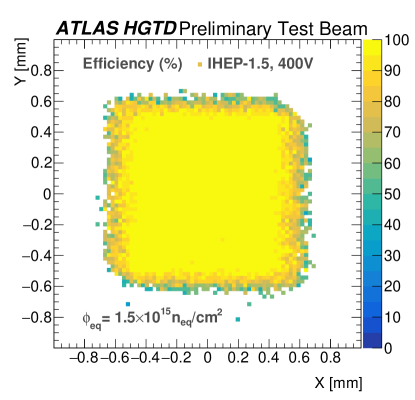
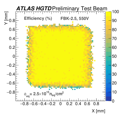
Figures 10 (a) and 10 (b) show the two-dimesional (2D) map of the efficiency as a function of the hit position for the IHEP-1.5 sensor (figure (a)) and the FBK-2.5 sensor (figure (b)). Both sensors were tested at DESY with a 5 GeV electron beam. They were enclosed in a styrofoam box, filled with dry ice, which was moving upwards during data taking due to the evaporation of the dry ice. Movements, temperature variation, and other factors may contribute to the smeared figures.
 |
 |
| (a) | (b) |
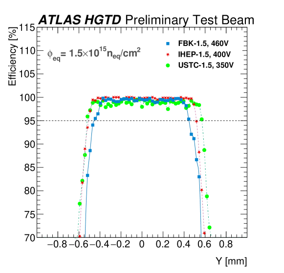
For more details, figure 11 shows the uniformity of the efficiency along the y-axis for the sensors irradiated at a fluence of neq/cm2 and tested at DESY with a electron beam. The efficiency of the sensor USTC-1.5 shows some variation up to 1.5% of the mean efficiency on the plateau. Figure 11 also allows to extract the size of the region where the efficiency was larger than 99.8% of the efficiency computed in the center of the DUT. These sizes are given in table 3 for the three sensors. Table 3 also gives the size of the region where the efficiency is larger than 95%, which is the required efficiency for irradiated sensors. These numbers can be compared to the nominal surface of 1.31.3 of the DUTs.
| Sensors | Bias Voltage | Temperature | Efficiency | Size of the plateau | |
| [V] | [] | in the DUT center | at 99.8% of | if eff > 95% | |
| [%] | DUT eff [m] | [m] | |||
| FBK-1.5 | 460 | -32 | 99.4 | 740 | 863 |
| USTC-1.5 | 350 | -33 | 98.9 | 937 | 1085 |
| IHEP-1.5 | 400 | -38 | 99.8 | 888 | 987 |
6 Conclusion and outlook
The High Granularity Timing Detector requires high-performance and radiation-resistant sensors. LGADs have been studied both in terms of radiation resistance and performance. Beam test campaigns have led us to choose promising technologies studied in this paper. Carbon-enriched LGAD samples from three vendors were considered: FBK, IHEP-IME and USTC-IME. The LGADs were irradiated to simulate their end-of-life state and studied under particle beams at DESY and CERN in 2021 and 2022.
Although irradiated at fluences of to neq/cm2, the LGADs presented in this paper were operated at voltages below . Under these conditions, they achieved the objectives of a collected charge of more than while guaranteeing an optimum time resolution below . An efficiency larger than 95% uniformly over the sensor’s surface is obtained with a charge threshold of . These results confirm the feasibility of an LGAD-based timing detector for HL-LHC.
Acknowledgements
The authors gratefully acknowledge CERN and the SPS staff for successfully operating the North Experimental Area and for continuous supports to the users. Measurements leading to the SPS results have been carried out using a MALTA beam telescope as part of the CERN ATLAS R&D programme. The authors thank MALTA team for their successful running of the telescope during the data-taking. The measurements leading to these results have been performed at the Test Beam Facility at DESY Hamburg (Germany), a member of the Helmholtz Association (HGF). The authors gratefully acknowledge DESY staff for their support to the users. This work was partially funded by MINECO, Spanish Government, under grant RTI2018-094906-B-C21. This project has received funding from the European Union’s Horizon 2020 research and innovation programme under the Marie Sklodowska-Curie grant agreement No. 754510. This work was partially funded by: the Spanish Government, under grant FPA2015-69260-C3-2-R and SEV-2012-0234 (Severo Ochoa excellence programme); and by the H2020 project AIDA-2020, GA no. 654168. This work is partially supported by “the Fundamental Research Funds for the Central Universities” of China (grant WK2030040100), the National Natural Science Foundation of China (No. 11961141014) and the Chinese Academy of Sciences (Grant NO. : GJJSTD20200008).
References
- [1] ATLAS Collaboration, Technical Proposal: A High-Granularity Timing Detector for the ATLAS Phase-II Upgrade, tech. rep. CERN-LHCC-2018-023, CERN, (2018) https://cds.cern.ch/record/2623663.
- [2] ATLAS Collaboration, Technical Design Report: A High-Granularity Timing Detector for the ATLAS Phase-II Upgrade CERN-LHCC-2020-007, CERN, (2020) ATLAS-TDR-031. https://cds.cern.ch/record/2719855.
- [3] ATLAS Collaboration, The ATLAS Experiment at the CERN Large Hadron Collider, JINST 3 (2008) S08003.
- [4] O. Brüning, L. Rossi et al., High Luminosity Large Hadron Collider: A description for the European Strategy Preparatory Group, Tech. Rep. CERN-ATS-2012-236 (2012).
- [5] A. G. et al., High-Luminosity Large Hadron Collider (HL-LHC): Technical Design Report V.0.1, CERN Yellow Reports: Monographs, CERN, (2017) http://cds.cern.ch/record/2284929.
- [6] G. Pellegrini et al., Technology developments and first measurements of Low Gain Avalanche Detectors (LGAD) for high energy physics applications, Nucl. Instrum. Meth. A 765 (2014) 12, https://doi.org/10.1016/j.nima.2014.06.008.
- [7] C. De La Taille et al., ALTIROC0, a 20 pico-second time resolution ASIC for the ATLAS High Granularity Timing Detector (HGTD) in Proceedings of the Topical Workshop on Electronics for Particle Physics (TWEPP-17), Santa Cruz, California, U.S.A, September 2017, PoS TWEPP-17 (2018) 006.
- [8] L. Masetti et al., Beam test measurements of Low Gain Avalanche Detector single pads and arrays for the ATLAS High Granularity Timing Detector, JINST 13 (2018) P06017, arXiv:1804.00622.
- [9] C. Agapopoulou et al., Performance of a Front End prototype ASIC for picosecond precision time measurements with LGAD sensors, JINST 15 (2020) P07007, arXiv:2002.06089.
- [10] J. Lange et al., Gain and time resolution of thin Low Gain Avalanche Detectors before and after irradiation up to a fluence of 1015 neq/cm2, JINST 12 (2017) P05003, arXiv:1703.09004.
- [11] C. Agapoupoulou et al., Performance in beam tests of irradiated Low Gain Avalanche Detectors for the ATLAS High Granularity Timing Detector, JINST 17 (2022) P09026, https://dx.doi.org/10.1088/1748-0221/17/09/P09026.
- [12] L. Castillo García, E. L. Gkougkousis, C. Grieco, S. Grinstein, Characterization of Irradiated Boron, Carbon-Enriched and Gallium Si-on-Si Wafer Low Gain Avalanche Detectors, Instruments 6 (2022) 1-2, https://doi.org/10.3390/instruments6010002.
- [13] M. Ferrero et al., Radiation resistant LGAD design, Nucl. Instrum. Meth. A 919 (2019) 16-26, https://doi.org/10.1016/j.nima.2018.11.121.
- [14] N. Cartiglia et al., Design optimization of ultra-fast silicon detectors, Nuclear Instruments and Methods in Physics Research A 796 (2015) 141–148.
- [15] V. Sola et al., Ultra-Fast Silicon Detectors for 4D tracking, Journal of Instrumentation 12 (2017) C02072.
- [16] H. F.-W. Sadrozinski, A. Seiden, N. Cartiglia, 4-Dimensional Tracking with Ultra-Fast Silicon Detectors, Reports on Progress in Physics 81 (2018) 026101.
- [17] S. M. Mazza et al., Tuning of gain layer doping concentration and Carbon implantation effect on deep gain layer, https://doi.org/10.48550/arXiv.2201.08933.
- [18] K. Wu et al., Design and testing of LGAD sensor with shallow carbon implantation, https://doi.org/10.48550/arXiv.2205.05025.
- [19] X. yang et al, Recent results of the carbonated USTC-IME LGADs and fabrication of the AC-LGADs at USTC NRFC, https://indico.cern.ch/event/1157463/contributions/4922750/.
- [20] R.Diener, J.Dreyling-Eschweiler, H.Ehrlichmann, I.M.Gregor, U.Kötz, U.Krämer, N.Meyners, N.Potylitsina-Kube, A.Schütz, P.Schütze, M.Stanitzki, The DESY II test beam facility, Nucl. Instr. Meth. A 922 (2019) Pages 265–286.
- [21] CERN SPS North Area: http://sba.web.cern.ch/sba/BeamsAndAreas/H6/H6_presentation.html.
- [22] Z. Galloway et al., Properties of HPK UFSD after neutron irradiation up to neq/cm2, Nucl. Instr. Meth. A 940 (2019) Pages 19–29.
- [23] H.Jansen, S.Spannagel, J.Behr, A.Bulgheroni, G.Claus, E.Corrin, D.Cussans, J.Dreyling-Eschweiler, D.Eckstein, T.Eichhorn, et al., Performance of the EUDET-type beam telescopes, EPJ Techniques and Instrumentation 3 (2016), doi:10.1140/epjti/s40485-016-0033-2, arxiv:1603.09669v2.
- [24] U. Koetz, I. Rubinskiy, User Manual: ATLAS FE-I4A Pixel Module as a Trigger Plane for the Beam Telescope, https://telescopes.desy.de/images/0/08/131014_koetz-rubinsky_FEI4_as_trigger_plane.pdf.
- [25] D. Cussans, Description of the JRA1 Trigger Logic Unit (TLU), v0.2c, Tech. Rep., (2009), http://www.eudet.org/e26/e28/e42441/e57298/EUDET-MEMO-2009-04.pdf.
- [26] M. Dyndal et al., Mini-MALTA: Radiation hard pixel designs for small-electrode monolithic CMOS sensors for the high luminosity LHC, JINST, 15 (2020) P02005.
- [27] Kiehn, Moritz, Proteus beam telescope reconstruction (v1.4.0). Zenodo. (2009) https://doi.org/10.5281/zenodo.2586736.
- [28] G. Laštovička-Medin et al., A brief overview of the studies on the irreversible breakdown of LGAD testing samples irradiated at the critical LHC-HL fluences, JINST 17 (2022) C07020, https://doi.org/10.1088/1748-0221/17/07/C07020.