Topological insulator spin transistor
Abstract
When a charge current is injected into the surface state of a topological insulator (TI), the resulting shift of the spin-momentum-locked Fermi surface leads to the appearance of a net spin polarization. The helical spin structure of the Dirac-cone surface state of a TI should lead to a fixed sign of this spin polarization for a given current direction, but experimentally, both signs that agree and disagree with the theory expectation for the surface state Dirac cone have been observed in the past. Although the origin of the wrong sign has not been conclusively elucidated, this observation points to the possibility that one may switch the spin polarization at will to realize a spin transistor operation. Here we report the observation of both signs of spin polarization in the very same device and demonstrate the tunability between the two by electrostatic gating, which gives a proof of principle of a topological insulator spin transistor. This switching behaviour is explained using a minimal model of competing contributions from the topological surface state and trivial Rashba-split states.
I Introduction
A Datta-Das spin transistor [1] can be an energy-efficient alternative of the traditional transistor and it represents one of the crucial components in spintronics [2, 3]. Instead of tuning the carrier density in a traditional field-effect transistor, in a spin transistor the gate acts on the spin degree of freedom of electrons. The main component of a Datta-Das spin transistor is a material with strong Rashba spin-orbit coupling [1]. Significant efforts have been devoted to realize this type of spin transistor [4, 5], most notably on a gated 2-dimensional (2D) electron gas [4]. In this context, topological insulators (TIs) arise as a promising class of materials for spintronics [6, 7, 8, 9, 10, 11, 12, 13, 14, 15, 16, 17] due to the helical spin-momentum locking in their surface state [18] and spin transistor would be an interesting application of TIs [13, 19].
When a charge current is injected into the surface state of a TI, the resulting shift of the Fermi surface leads to a net spin imbalance in the current-carrying electrons, which is called Edelstein effect [20]. This allows for generating a spin-polarized current without the need of a ferromagnetic (FM) spin source. In the past, multiple methods for the detection of this current-induced spin polarization (CISP) have been proposed and experimentally realized [6, 21, 22, 23, 24]. Among these methods, using a FM potentiometer to probe the spin polarization as a spin voltage [25] is convenient, as it enables simple electrical detection of the gate-induced sign change of the CISP, which is the key signature of the spin transistor operation presented in this paper.
In the topological surface state (TSS) of TIs, the helicity of the spin polarization changes sign across the Dirac point (DP) [18]. Hence, at first sight, one might expect that tuning the chemical potential across the DP by electrostatic gating can easily reverse the surface spin polarization in a current-biased TI. However, the Fermi velocity of the surface electrons also changes sign at the DP, which results in the same spin polarization for the same direction of the applied current. This mechanism has been explained in detail by Yang et al. [13]. In other words, in TIs, the helicity of their TSS allows only one type of spin polarization that is determined by the sign of the applied current. Indeed, the expected sign of the CISP has been observed in many experiments [7, 8, 10, 11, 12, 13, 14, 15].
However, the opposite sign of the CISP has also been reported in TI devices [6, 13, 26] and this must be explained by a different physical mechanism other than the current-carrying TSS electrons. The origin of this anomalous CISP has been a topic of interest and several possible explanations have been proposed, including bulk spin Hall effect [26], Rashba-split states [27, 13], and spin-dependent interface resistance [28]. Unfortunately, no decisive evidence of any of these explanations have been found experimentally, leaving the origin of the opposite CISP ambiguous. Nevertheless, it has been remarked that devices with a higher carrier density (hence a higher chemical potential) tend to exhibit the unexpected CISP [13, 26]. Regardless of its origin, the existence of the CISP of opposite sign in devices with a higher chemical potential suggests that it may be possible to control the sign fo the CISP with electrostatic gating, thus realizing a spin transistor operation in a TI [13]. So far, while a gate-tunability of the amplitude of the CISP (showing a peak near the DP) has been reported [12], the gate-induced switching of the CISP has not been achieved [12, 26].
For the purpose of controlling the sign of the spin voltage with electrostatic gating, in this study we base our devices on TI flakes that were exfoliated to the thicknesses of less than 20 nm in order to achieve a sizeable tunability of the top TSS from bottom gating. Secondly, we used bulk crystals of Bi2-xSbxTe3-ySey (BSTS) with different compositions to obtain different chemical potentials at zero gate voltage. Upon gating, we observed a maximum in the CISP near the DP in one device and sign switching of the CISP, with complicated multiple-switching behaviour, in two other devices. Furthermore, we provide a theoretical explanation of this switching behaviour based on the assumption that the opposite sign of the CISP originates from trivial Rashba-split states on the surface of a TI.
II Experimental Results
II.1 Devices for spin voltage detection
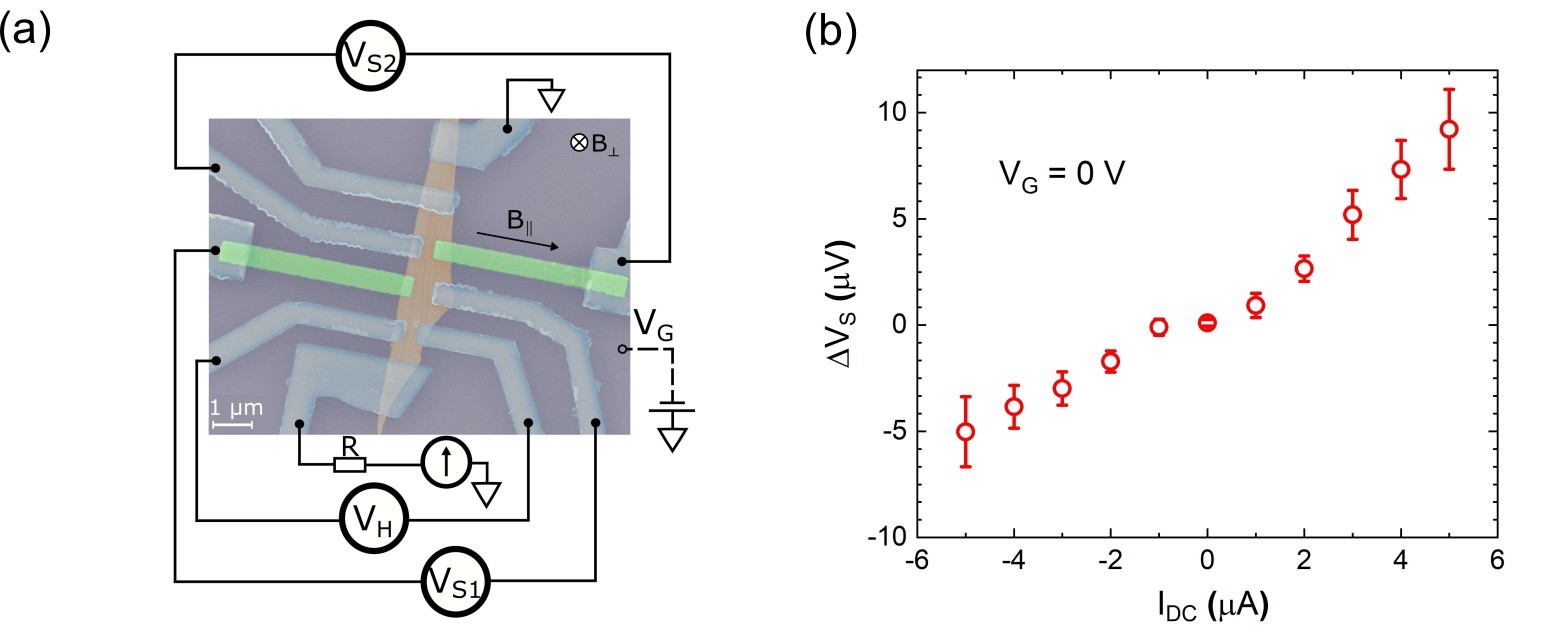
For all of the analyzed devices, the voltage measured between the Py lead and its reference lead, which reflects the relative orientations of the spins in Py and in the TI surface, shows a clean hysteresis as a function of with a coercive field of about 20 Oe as expected for a thin (30 nm) Py strip that is magnetized along its easy axis (see Fig. 1a for device schematics). In contrast to previous experiments where averaging of multiple sweeps was required to extract the hysteresis [7, 13], here, we could resolve it even from a single magnetic field sweep due to an enhanced signal-to-noise ratio and reduced charge fluctuations. The latter owes to a better tunnel barrier made of SiNx (see Methods section for details). The size of the voltage hysteresis, i.e. the spin voltage which is proportional to the CISP on the TI surface, shows an approximate linear dependence on the applied current (Fig. 1b) and changes sign upon reversal of the current direction, as expected. The spin resistance in device A is similar to previously reported values in the range of 1–5 [15, 28, 10]
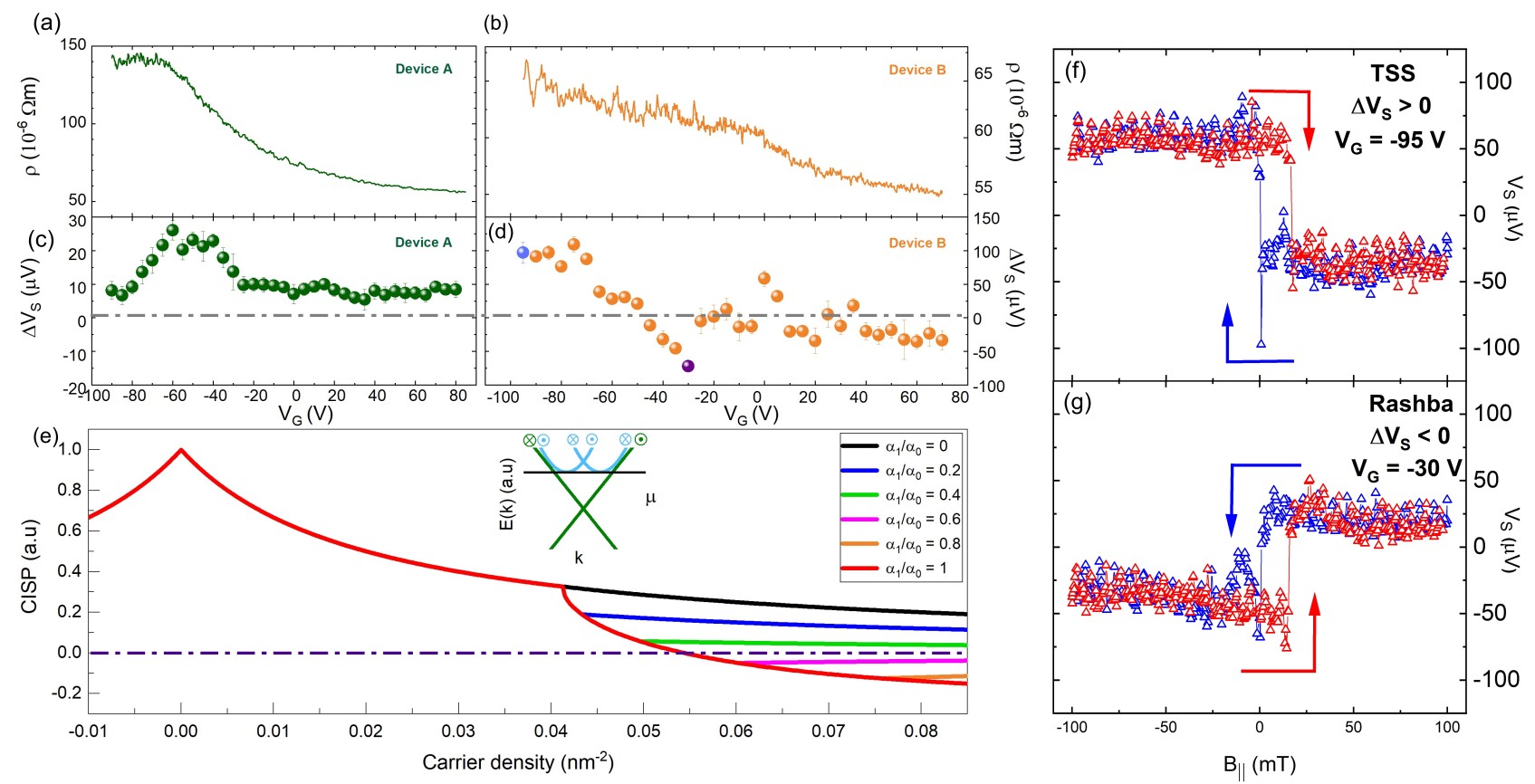
Next, we turn to the dependence of the spin voltage on the chemical potential (gate voltage) to study the different signs that have been reported. Here, for the first time we observed both signs of the spin voltage in a single device upon changing the gate voltage (Figs. 2f and 2g). However, before discussing the devices presenting the sign reversal, we first consider the reference device A (Fig. 2a). The TI flake used for device A was bulk-insulating and the chemical potential can be tuned to the DP with a gate voltage V, as reflected in a resistance peak of the longitudinal resistivity . Similarly, also presents a maximum, but at a slightly different gate voltage V (Fig. 2c). Even though is expected to be maximum when the chemical potential is at the DP [12], a finite difference between and may originate from the fact that both the top and bottom TSSs contribute to the resistance of the flake, while only the top TSS contributes to the spin voltage. These two TSSs experience different chemical potential tuning by the gate. Tuning the gate away from the spin voltage peak, decays quickly and saturates for V, which fits well with the expectation for a single Dirac cone contribution to spin polarization [29, 24]. From an estimation of the geometric capacitance of the gate for this device, the conduction band edge is expected to be reached at a gate voltage V. Since the Rashba-split band is formed very close to the conduction band edge, one expects the onset of its contribution at this voltage. The absence of clear features in around 60 V is explained by screening effects or by an electric field-induced suppression of the Rashba splitting due to the large gate voltage that is required to tune to the conduction band (see below for details).
II.2 Gate-controlled sign reversal of the spin voltage
To better access the Rashba-split band, another device B was fabricated from a more n-type TI flake, such that a smaller gate voltage suffices to tune the chemical potential to the conduction band. In this device, the spin voltage indeed shows a much richer gate response (Fig. 2d). The dependence of in this device (Fig. 2b) shows n-type behaviour with smaller absolute values of and a reduced gate tunability, both indicating that the chemical potential in this device without gating is closer to the conduction band. Comparing the resistivity values of this device to device A, a rough estimate of a gate voltage shift between device A and device B of about 50 V can be deduced. Consistent with this estimate, the resistance cannot be tuned to a peak within the gate voltage range accessible in our experiment and the device remains n-type. Interestingly, the spin voltage of device B shows multiple sign switches (below we show we can attribute a positive or negative sign of to the TSS or trivial Rashba bands, respectively). At large negative gate voltages, the positive sign is consistent with a dominant TSS contribution. Upon sweeping to the positive direction, however, drops abruptly near V and a sign reversal occurs close to V, indicating the appearance of another contribution and eventual reversal of the spin polarization. With further sweeping of to the positive direction, the sign of switches a couple of times and eventually converges to a negative value at 40 V. Even though seemingly fluctuates between plus and minus, it should be noted that for a given fixed gate voltage, the hysteresis loops such as shown in Figs. 2f and 2g are static and reproducible. Yet, their sign can invert quickly with a small change in the gate voltage. In other words, the dependence of reflects an intrinsic property that changes rapidly within a certain gate-voltage range and it is not the result of a random fluctuation or instability. Here, the opposite spin polarization was observed at different gate voltages in the same device, which has not been reported before in this type of TI-based devices.
Notably, the spin voltage reversal was observed in the more n-type device B, while it was completely absent in device A. The absence of Rashba contributions upon gating in device A could be explained in two ways. First, due to the screening effect from the FM lead, the chemical potential underneath the lead is not efficiently tuned by the electrostatic gate. Therefore, even at a gate voltage high enough to bring a crystal of similar pristine carrier density to the conduction band, the chemical potential in device A may still resides in the bulk gap. Second, it is known that a strong electric field can affect the splitting of a Rashba-split state [30], effectively changing (or even reversing) its contribution to the spin polarization. In device A, the chemical potential is closer to the DP without gating, hence a larger gate voltage (i.e. a large electric field) is required to bring the chemical potential to the conduction band edge. This large electric field can then weaken the contribution from the Rashba band to the spin polarization, leading to the absence of an opposite spin polarization in device A. Both mechanisms can be circumvented by employing a crystal with a higher pristine chemical potential. Indeed, device B as well as device C (see Supplemental information), which were fabricated from such a crystal (see Methods), exhibit the Rashba-type contribution, i.e., the sign reversal of .
II.3 Effects of chemical potential pinning by Py and spin diffusion
One of the previous explanations of the unexpected sign of the spin voltage was based on the contribution of the trivial Rashba-split states formed underneath the metallic ferromagnetic contacts due to band bending [13]. However, in this scenario one would expect that the chemical potential underneath the metal contacts, i.e. the spin detector, is fixed and cannot be changed with the gate. Thus, at first sight, one might not expect any gate dependence of the spin voltage from this area at all. However, our data clearly shows that the spin voltage detected is gate-tunable: Device A exhibits a peak in near the DP, indicating that the chemical potential of the spin-polarized electrons is indeed modified and can be brought to the DP. If the CISP would originate from electrons underneath the FM leads alone, this should not happen. This contradiction may be resolved by considering spin diffusion from the (free) area not covered by the FM leads to the area underneath the FM leads. These two areas differ in terms of the electronic states and the gate tunability: In the free area, the chemical potential is not pinned, but can be tuned by the bottom gate via the electrostatic coupling between the top and bottom TSSs [31]. In addition, Rashba-split states due to trivial surface states can be formed in the free area [32, 33, 34, 35]. Those may become visible in the CISP probed by the FM detector via spin diffusion. In the area beneath the FM lead, Rashba-split states would also exist due to band bending effects at the Py/TI interface and, even though the chemical potential is pinned here, the size of the Rashba splitting is modified by the electric field generated upon gating, leading to a modification of the CISP in this area as well [30, 13].
The spin voltage detected in the experiment reflects all of these sources of spin polarization via averaging the CISP in an area that is larger than the detector by an area set by the order of the spin diffusion length. Typical spin diffusion lengths in TI materials (up to 1 m, [36]) are of similar order as the size of the present FM detector, such that the observed CISP can be understood as simply the average of the contributions from the two areas.
III Theoretical understanding of the spin transistor effect
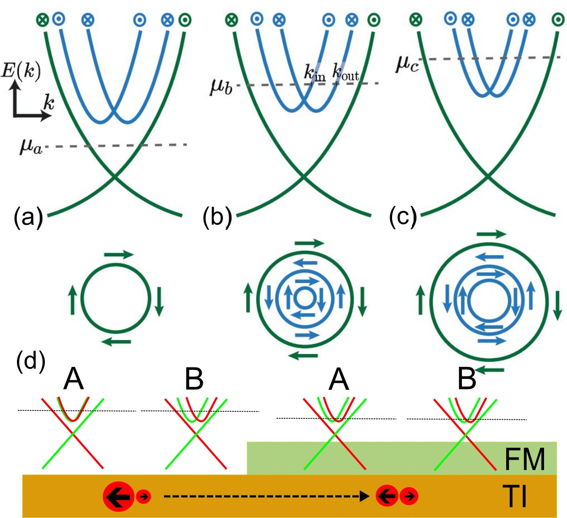
The mechanism of the spin transistor effect is graphically demonstrated in Fig. 3d, which depicts the different behaviour of devices A and B. In device A, for bringing the chemical potential into the Rashba states of the free area, a very large gate voltage is required, which significantly reduces the Rashba coefficient such that there is no sizeable contribution of Rashba-type to the detected CISP. Additionally, the Rashba states formed underneath the FM may contribute as well, but the magnitude is mostly set by the details of the FM/TI interface and the tunability by the gate is limited. In the more n-type device B (and in device C, see Supplementary Information) the Rashba splitting in the free area remains large enough upon gate tuning to induce a negative contribution to the CISP.
The key features of the CISP observed in our experiment can be described with a minimal model that includes the contributions from both the topological surface state and surface Rashba states. We consider a simple Hamiltonian for the surface of our TI, such that
| (1) |
here and are Pauli matrices in spin-space, is a diagonal matrix in band-space that distinguishes the th band, is the effective mass of this band, governs the crossing point of this band, and is the chemical potential. In particular, we label the topological surface state by such that and measure the chemical potential from the Dirac point such that . Note that throughout we set . Importantly, we set the parameters of this model all of the same sign, such that the Rashba parameters of the trivial surface states are consistent with the sign of the helicity of the topological surface state (see Fig. 3).
Within this simple model, the CISP due to an electric field can be written as [15] (see Methods for full details)
| (2) |
where is the spin-up(down) density and is the total density. The contribution from the topological surface state is
| (3) |
where is the impurity strength. Similarly, the Rashba surface state () contributions are of opposite sign and take the form
| (4) |
where ( are the outer (inner) Fermi-momenta of the th Rashba surface band (see Fig. 3). We also defined the scattering time for each band, , and in the approximation we assume that only intraband scattering is relevant, such that is governed by the impurity strength, , and the density of states of the band .
The situations of the bands reflecting the effects of increasing gate-induced electric field are depicted in Figs. 3a-3c. As expected, when the chemical potential is in the vicinity of the Dirac point, the CISP is entirely dominated by the contribution of the surface state. However, when the chemical potential is tuned close to the edge of the bulk conduction band, trivial Rashba surface state(s) result in a contribution to the CISP which has the opposite sign and therefore can cause a total sign change of the CISP if (see Fig. 2e).
Finally, we comment on how the full experimental behaviour, including multiple sign changes far from the Dirac point, can be understood within this simple model: If the contribution of the Rashba states, , are dependent on the chemical potential, several sign changes can occur in the vicinity of the bulk conduction band as the gate voltage is varied (see Fig. 3). In fact, such a dependence is quite natural. For instance, the Rashba strength can be modified by the electric field that arises due to gating [30] and/or the coefficient will in reality be dependent on momentum . Furthermore, the mass will have momentum dependent corrections that could also reduce the magnitude of . In contrast, it is known that the Fermi velocity, , of the topological surface Dirac cone increases close to the bulk conduction band and this will lead to a corresponding increase in the contribution , see Eq. (3). Hence, the relative magnitudes of the topological and trivial CISP contributions can explain the multiple switches observed experimentally. The full understanding of this multiple switchings behaviour is an important subject for the future applications of topological insulator spin transistors.
IV Conclusion
We studied the gate-voltage dependence of CISP in different devices fabricated from Bi2-xSbxTe3-ySey crystals. We observed gate-controlled sign reversals of the CISP for the first time in TI devices and such sign reversals were found to occur only in devices fabricated from n-type crystals. We argue that trivial Rashba-split states on the TI surface contributes to the CISP with an opposite sign compared to that from the TSS and the dependence of the Rashba parameter on the electric field generated by the back gate plays a crucial role in their competition, leading to complicated sign reversals in the observed CISP as a function of the gate voltage. Our devices demonstrate the feasibility of the spin transistor conceived by Yang et al. in Ref. [13], while presenting the importance of spin diffusion in its working principle. The spin transistor effect demonstrated here will significantly widen the prospect of TIs for spintronic applications. For fundamental research, the miniaturization of the spin transistor into the ballistic transport regime would be extremely interesting, because the efficiency of the CISP would be drastically enhanced compared to the diffusive transport regime [18].
V Acknowledgements
This work has received funding from the Deutsche Forschungsgemeinschaft (DFG, German Research Foundation) under CRC 1238-277146847 (subprojects A04 and B01) and under 398945897, as well as under Germany’s Excellence Strategy – Cluster of Excellence Matter and Light for Quantum Computing (ML4Q) EXC 2004/1-390534769. H. F. Legg acknowledges support by the Georg H. Endress Foundation.
Apendix
Device fabrication:
The data shown in this paper were taken on three different devices A,B and C. Two different TI crystals were used for device fabrication: device A was fabricated from BiSbTeSe2 bulk crystal, while device B and C were fabricated from Bi1.5Sb0.5Te1.3Se1.7 crystal with a chemical potential closer to conduction band edge compared to the former. Both single crystals were grown by the modified Bridgman method. TI flakes were exfoliated from single crystals using standard scotch tape technique onto degenerately doped Si substrates coated by a 290-nm layer of SiO2 acting as a gate dielectric. Thin flakes ( 20 nm) with a suitable shapes and sizes and flat surfaces were selected using optical microscopy. After exfoliation the substrate was immediately loaded to the vacuum chamber of the HW-CVD machine to minimize any native oxide formation on the TI surface. There, a 1-nm-thick layer of SiNx was deposited on top of TI, acting as a capping layer and tunnel barrier at the same time. During the SiNx deposition, the substrate temperature was observed to stay below 100∘C. Diluted ZEP 520A resist was spin coated immediately after the SiNx deposition. Electron beam lithography was performed using a Raith Pioneer Two system. Contacts were fabricated using Niobium (Nb) and Permalloy (Py) for the normal and FM contacts, respectively, by a liftoff-technique. For normal leads, first the SiNx layer was removed using reactive ion etching in CF4 plasma, followed by the deposition of 35-nm-thick Nb via magnetron sputtering. In a second lithography, 30-nm-thick Py leads were deposited by thermal evaporation without removing the SiNx layer. The tunnel-barrier resistances of the measured FM leads of device A, B and C were 4.2, 4.1 and 6.4 , respectively. Finally, 40-nm-thick Nb leads were fabricated to connect to pre-patterned Au bonding pads.
Measurements:
All measurements were performed in Oxford Instruments TRITON 200 dilution refrigerator at the base temperature of 20–40 mK. A vector magnet was used to allow measurement of multiple devices with different orientations in the same run. The wiring scheme of the spin voltage measurement is illustrated in Fig. 1a. DC current is applied using the two outer Nb contacts and an in-plane magnetic field mT is applied along the easy axis of the FM contact to switch its magnetization. The voltage is measured between a FM lead and the opposing Nb lead as a function of the magnetic field using a Keithley 2182A nanovoltmeter; this contact arrangement minimizes the contribution of the longitudinal resistance. Further data treatments to subtract the remaining longitudinal resistance contribution is described in the Supplementary Information. The back-gate voltage is applied to the sample using a Keithley 2450 sourcemeter. Each measurement includes multiple forward (negative to positive ) and backward (positive to negative ) magnetic-field scans. An average is deduced from multiple scans for each biased current or gate voltage to reduce the noise. The longitudinal resistance was measured in a standard 4-probe configuration with a low-frequency (13.77 Hz) AC technique using a NF LI5640 lock-in amplifier.
Calculation of the current-induced spin polarization:
First, to connect with the experimental gate voltage dependence of the CISP, we make the simplifying assumption that the capacitance is independent of chemical potential and that the gate voltage changes only the surface density. Using Luttinger’s theorem we obtain this density, such that
| (5) |
where encodes the fact that in any real experimental setup there is a contribution from bulk impurity states to the density , this prevents the divergence of the CISP when the chemical potential is at the Dirac point. This equation can be used to obtain because we calculate the CISP (below) for a given chemical potential.
We now derive Eq. (2), namely, the contributions of each individual Fermi-pocket (shown in Fig. 3b) to the CISP. Using the Boltzmann description [15], we can write the occupation function in the presence of an electric field , to linear order, as . For a given chemical potential the contribution to the spin density of a Fermi surface with helicity is given by
| (6) |
where the inner and outer Fermi-pockets always have opposite helicity (see Fig. 3). Hence the difference in spin density for a single pair of bands , as appears in the CISP, is given by
| (7) |
where for the topological band because there is only the inner Fermi-pocket.
Finally, to calculate the CISP (the result of which is shown in Fig. 2e), we need to approximate the transport scattering time, , for the th pair of bands. We do this by assuming only intra-Fermi pocket scattering is relevant, such that the scattering rate is given by
| (8) |
where is the density of states of the given Fermi pocket for the th band. For the topological Fermi pocket and for trivial Fermi pocket . Inserting these scattering times into gives the approximations in Eq. (3) and Eq. (4). In reality, inter-pocket scattering will also occur and this would couple all bands. However, our simple approximation using only intra-pocket scattering is sufficient to capture the change of sign in the CISP observed in our experiment.
References
- Datta and Das [1990] S. Datta and B. Das, Electronic analog of the electro-optic modulator, Appl. Phys. Lett. 56, 665 (1990).
- Žutić et al. [2004] I. Žutić, J. Fabian, and S. D. Sarma, Spintronics: Fundamentals and applications, Rev. Mod. Phys. 76, 323 (2004).
- Awschalom and Flatté [2007] D. D. Awschalom and M. E. Flatté, Challenges for semiconductor spintronics, Nat. Phys. 3, 153 (2007).
- Chuang et al. [2015] P. Chuang, S.-C. Ho, L. W. Smith, F. Sfigakis, M. Pepper, C.-H. Chen, J.-C. Fan, J. Griffiths, I. Farrer, H. E. Beere, et al., All-electric all-semiconductor spin field-effect transistors, Nat. Nanotechnol. 10, 35 (2015).
- Ingla-Aynés et al. [2021] J. Ingla-Aynés, F. Herling, J. Fabian, L. E. Hueso, and F. Casanova, Electrical control of valley-zeeman spin-orbit-coupling–induced spin precession at room temperature, Phys. Rev. Lett. 127, 047202 (2021).
- Li et al. [2014] C. Li, O. Van‘t Erve, J. Robinson, Y. Liu, L. Li, and B. Jonker, Electrical detection of charge-current-induced spin polarization due to spin-momentum locking in Bi2Se3, Nat. Nanotechnol. 9, 218 (2014).
- Ando et al. [2014] Y. Ando, T. Hamasaki, T. Kurokawa, K. Ichiba, F. Yang, M. Novak, S. Sasaki, K. Segawa, Y. Ando, and M. Shiraishi, Electrical detection of the spin polarization due to charge flow in the surface state of the topological insulator Bi1.5Sb0.5Te1.7Se1.3, Nano Lett. 14, 6226 (2014).
- Tang et al. [2014] J. Tang, L.-T. Chang, X. Kou, K. Murata, E. S. Choi, M. Lang, Y. Fan, Y. Jiang, M. Montazeri, W. Jiang, Y. Wang, L. He, and K. Wang, Electrical detection of spin-polarized surface states conduction in (Bi0.53Sb0.47)2Te3 topological insulator, Nano Lett. 14, 5423 (2014).
- Liu et al. [2015] L. Liu, A. Richardella, I. Garate, Y. Zhu, N. Samarth, and C.-T. Chen, Spin-polarized tunneling study of spin-momentum locking in topological insulators, Phys. Rev. B 91, 235437 (2015).
- Tian et al. [2015] J. Tian, I. Miotkowski, S. Hong, and Y. P. Chen, Electrical injection and detection of spin-polarized currents in topological insulator Bi2Te2Se, Sci. Rep. 5, 1 (2015).
- Dankert et al. [2015] A. Dankert, J. Geurs, M. V. Kamalakar, S. Charpentier, and S. P. Dash, Room temperature electrical detection of spin polarized currents in topological insulators, Nano Lett. 15, 7976 (2015).
- Lee et al. [2015] J. S. Lee, A. Richardella, D. R. Hickey, K. A. Mkhoyan, and N. Samarth, Mapping the chemical potential dependence of current-induced spin polarization in a topological insulator, Phys. Rev. B 92, 155312 (2015).
- Yang et al. [2016] F. Yang, S. Ghatak, A. Taskin, K. Segawa, Y. Ando, M. Shiraishi, Y. Kanai, K. Matsumoto, A. Rosch, and Y. Ando, Switching of charge-current-induced spin polarization in the topological insulator BiSbTeSe2, Phys. Rev. B 94, 075304 (2016).
- Vaklinova et al. [2016] K. Vaklinova, A. Hoyer, M. Burghard, and K. Kern, Current-induced spin polarization in topological insulator–graphene heterostructures, Nano Lett. 16, 2595 (2016).
- Li et al. [2016] C. H. Li, O. M. van‘t Erve, S. Rajput, L. Li, and B. T. Jonker, Direct comparison of current-induced spin polarization in topological insulator Bi2Se3 and InAs rashba states, Nat. Commun. 7, 1 (2016).
- Li et al. [2019a] P. Li, J. Kally, S. S. Zhang, T. Pillsbury, J. Ding, G. Csaba, J. Ding, J. S. Jiang, Y. Liu, R. Sinclair, C. Bi, A. DeMann, G. Rimal, W. Zhang, S. B. Field, J. Tang, W. Wang, O. G. Heinonen, V. Novosad, A. Hoffmann, N. Samarth, and M. Wu, Magnetization switching using topological surface states, Sci. Adv. 5, eaaw3415 (2019a).
- He et al. [2022] Q. L. He, T. L. Hughes, N. P. Armitage, Y. Tokura, and K. L. Wang, Topological spintronics and magnetoelectronics, Nat. Mater. 21, 15 (2022).
- Ando [2013] Y. Ando, Topological insulator materials, J. Phys. Soc. Jpn. 82, 102001 (2013).
- Bandyopadhyay [2022] S. Bandyopadhyay, Strained topological insulator spin field effect transistor, arXiv e-prints , arXiv:2210.13612 (2022), arXiv:2210.13612 [cond-mat.mes-hall] .
- Edelstein [1990] V. M. Edelstein, Spin polarization of conduction electrons induced by electric current in two-dimensional asymmetric electron systems, Solid State Commun. 73, 233 (1990).
- Shiomi et al. [2014] Y. Shiomi, K. Nomura, Y. Kajiwara, K. Eto, M. Novak, K. Segawa, Y. Ando, and E. Saitoh, Spin-electricity conversion induced by spin injection into topological insulators, Phys. Rev. Lett. 113, 196601 (2014).
- Yu et al. [2021] J. Yu, H. Zhuang, K. Zhu, Y. Chen, Y. Liu, Y. Zhang, C. Yin, S. Cheng, Y. Lai, K. He, et al., Observation of current-induced spin polarization in the topological insulator Bi2Te3 via circularly polarized photoconductive differential current, Phys. Rev. B 104, 045428 (2021).
- Hus et al. [2017] S. M. Hus, X.-G. Zhang, G. D. Nguyen, W. Ko, A. P. Baddorf, Y. P. Chen, and A.-P. Li, Detection of the spin-chemical potential in topological insulators using spin-polarized four-probe stm, Phys. Rev. Lett. 119, 137202 (2017).
- Leis et al. [2020] A. Leis, M. Schleenvoigt, A. R. Jalil, V. Cherepanov, G. Mussler, D. Grützmacher, F. S. Tautz, and B. Voigtländer, Room temperature in-situ measurement of the spin voltage of a BiSbTe3 thin film, Sci. Rep. 10, 1 (2020).
- Johnson and Silsbee [1988] M. Johnson and R. H. Silsbee, Coupling of electronic charge and spin at a ferromagnetic-paramagnetic metal interface, Phys. Rev. B 37, 5312 (1988).
- Tian et al. [2021] J. Tian, C. Şahin, I. Miotkowski, M. E. Flatté, and Y. P. Chen, Opposite current-induced spin polarizations in bulk-metallic Bi2Se3 and bulk-insulating Bi2Te2 Se topological insulator thin flakes, Phys. Rev. B 103, 035412 (2021).
- Hong et al. [2012] S. Hong, V. Diep, S. Datta, and Y. P. Chen, Modeling potentiometric measurements in topological insulators including parallel channels, Phys. Rev. B 86, 085131 (2012).
- Li et al. [2019b] C. H. Li, O. M. van‘t Erve, C. Yan, L. Li, and B. T. Jonker, Electrical detection of current generated spin in topological insulator surface states: Role of interface resistance, Sci. Rep. 9, 1 (2019b).
- Li and Appelbaum [2016] P. Li and I. Appelbaum, Interpreting current-induced spin polarization in topological insulator surface states, Phys. Rev. B 93, 220404 (2016).
- Caviglia et al. [2010] A. Caviglia, M. Gabay, S. Gariglio, N. Reyren, C. Cancellieri, and J.-M. Triscone, Tunable rashba spin-orbit interaction at oxide interfaces, Phys. Rev. Lett. 104, 126803 (2010).
- Fatemi et al. [2014] V. Fatemi, B. Hunt, H. Steinberg, S. L. Eltinge, F. Mahmood, N. P. Butch, K. Watanabe, T. Taniguchi, N. Gedik, R. C. Ashoori, et al., Electrostatic coupling between two surfaces of a topological insulator nanodevice, Phys. Rev. Lett. 113, 206801 (2014).
- Bianchi et al. [2010] M. Bianchi, D. Guan, S. Bao, J. Mi, B. B. Iversen, P. D. King, and P. Hofmann, Coexistence of the topological state and a two-dimensional electron gas on the surface of Bi2Se3, Nat. Commun. 1, 1 (2010).
- Zhu et al. [2011] Z.-H. Zhu, G. Levy, B. Ludbrook, C. Veenstra, J. Rosen, R. Comin, D. Wong, P. Dosanjh, A. Ubaldini, P. Syers, et al., Rashba spin-splitting control at the surface of the topological insulator Bi2Se3, Phys. Rev. Lett. 107, 186405 (2011).
- King et al. [2011] P. King, R. C. Hatch, M. Bianchi, R. Ovsyannikov, C. Lupulescu, G. Landolt, B. Slomski, J. Dil, D. Guan, J. Mi, et al., Large tunable rashba spin splitting of a two-dimensional electron gas in Bi2Se3, Phys. Rev. Lett. 107, 096802 (2011).
- Bahramy et al. [2012] M. Bahramy, P. King, A. De La Torre, J. Chang, M. Shi, L. Patthey, G. Balakrishnan, P. Hofmann, R. Arita, and N. Nagaosa, Emergent quantum confinement at topological insulator surfaces, Nat. Commun. 3, 1 (2012).
- Iyer et al. [2018] V. Iyer, Y. P. Chen, and X. Xu, Ultrafast surface state spin-carrier dynamics in the topological insulator Bi2Te2Se, Phys. Rev. Lett. 121, 026807 (2018).