Characterization of the response of IHEP-IME LGAD with shallow carbon to Gamma Irradiation
Abstract
Low Gain Avalanche Detectors (LGAD) for the High-Granularity Timing Detector (HGTD) are crucial in reducing pileups in the High-Luminosity Large Hadron Collider. Numerous studies have been conducted on the bulk irradiation damage of LGADs. However, few studies have been carried out on the surface irradiation damage of LGAD sensors with shallow carbon implantation. In this paper, the IHEP-IME LGADs with shallow carbon implantation were irradiated up to 2 MGy using gamma irradiation to investigate surface damage. Important characteristic parameters, including leakage currents, breakdown voltage (BV), inter-pad resistances, and capacitances, were tested before and after irradiation. The results showed that the leakage current and BV increased after irradiation, whereas overall inter-pad resistance exhibited minimal change and remained above before and after irradiation. Capacitance was found to be less than 4.5 pF with a slight decrease in the gain layer depletion voltage (Vgl) after irradiation. No parameter affected by the inter-pad separation was observed before and after irradiation. All characteristic parameters meet the requirements of HGTD, and this design can be used to further optimization.
1 Introduction
The Phase-II upgrade of the Large Hadron Collider (LHC), known as the High Luminosity LHC (HL-LHC), aims to achieve a luminosity of cm-2s-1, representing a ten-fold increase compared to the LHC[3, 2, 5]. This higher luminosity leads to significant pile-up effects, with an average of approximately 200 events, necessitating the implementation of a High-Granularity Timing Detector (HGTD) in the forward region of the ATLAS detector. The HGTD will incorporate a new type of silicon sensor, the Low Gain Avalanche Detector (LGAD), to enable precise timing measurements of charged tracks and aid in pile-up suppression [1].
LGAD is a type of silicon sensor that offers moderate internal gain, enabling enhanced signal amplitudes and achieving high time and spatial resolutions of better than 20 picoseconds and micrometers, respectively[13, 12, 10]. However, in the high-intensity beam and irradiation environments of the HL-LHC, LGADs are susceptible to various detrimental effects that can significantly impact their lifetime and performance [4, 13, 15]. To ensure the required irradiation hardness, the ATLAS committee has established stringent requirements for the detectors. The LGADs in the HGTD of ATLAS will not be replaced before the completion of half of the data taking of the HL-LHC (2000 fb-1). The anticipated total ionizing dose (TID) irradiation dose for the LGADs is expected to be 1.5 MGy[11].
Multiple institutes, including BNL, FBK, and NDL, have conducted studies on LGADs, investigating the effects of bulk damage caused by irradiation and observing numerous adverse effects on LGAD performance [7, 6, 14]. However, there has been limited research on surface damage specifically related to LGADs with carbon implantation [8]. This study aims to investigate the surface damage induced by gamma-ray irradiation on LGADs with shallow carbon implantation.
To achieve excellent irradiation hardness, the Institute of High Energy Physics (IHEP) collaborated with the Institute of Microelectronics (IME) to develop a new carbon-doped LGAD named IHEP-IME LGAD. This paper focuses on evaluating the performance of the third version of IHEP-IME LGAD (IHEP-IMEv3 LGAD, or v3) under 60Co gamma-ray irradiation with a maximum dose of 2 MGy. Such irradiation leads to surface damage at the SiO2 and Si-SiO2 interface, inducing oxide charges, interface traps, and point defects in the silicon sensors caused by Compton electrons and photoelectrons [16, 9]. The objective of this investigation is to optimize the surface parameters in LGAD design.
2 IHEP-IME LGAD sensors
LGAD samples used in this study were mainly taken from wafer 12 of v3. Some LGAD samples of the first version of IHEP-IME LGAD (IHEP-IMEv1 LGAD, or v1) were also taken. The structure of v3 from top to bottom is passivation layer, pad, SiO2, n++ layer, p+ layer (gain layer), p-type bulk, p++ layer and aluminum chuck as illustrated in Figure 1. In comparison to v3, v1 is also shallow carbon-doped LGAD, but it has not undergone surface passivation, which means it does not have the passivation layer shown in Figure 1. From an external perspective, v1 and v3 appear to be identical.
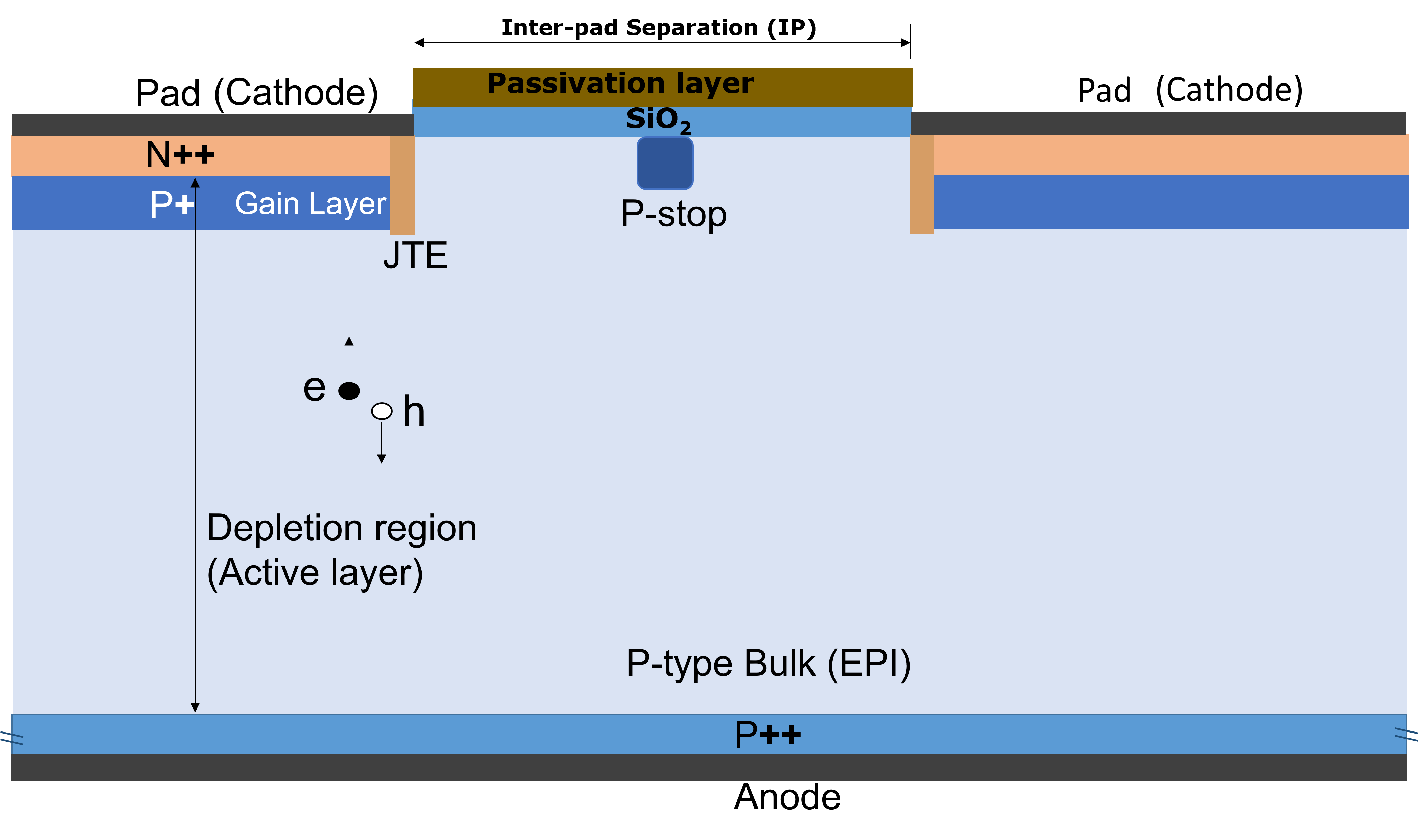
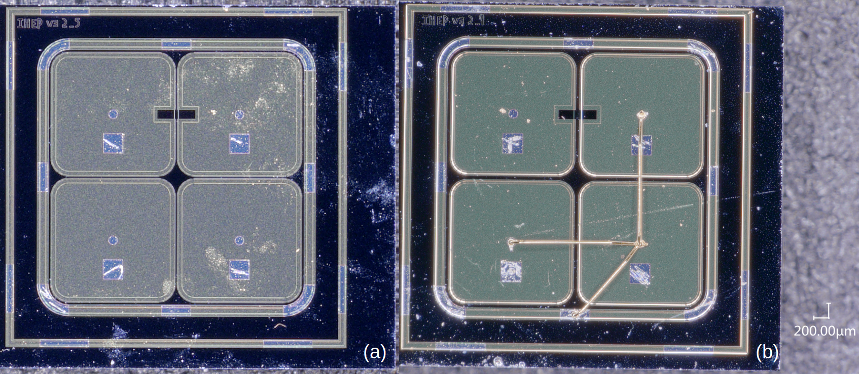
The thickness of p-type bulk is 50 m and of p++ layer is 725 m. A p-stop and JTEs between n++ and p+ layers are designed to reduce the lateral current, and all tested LGADs are quad square pad ( pads, 2 mm 2 mm for each pad) structures with different inter-pad separation (IP) from 50 m to 100 m, surrounded by guard-ring, as summarized in Table 1 and shown in Figure 2. Apart from the difference in IP, all other design parameters of the v3 sample are the same.
| Sample | Irradiation Dose (Gy) | IP () | Surface Passivation | Shallow Carbon | |
|---|---|---|---|---|---|
| 2-5 | 10k,100k,2M | 50 | Yes | Yes | |
| 2-6 | 10k,100k,2M | 60 | Yes | Yes | |
| 2-7 | 10k,100k,2M | 70 | Yes | Yes | |
| v3 | 2-8 | 10k,100k,2M | 80 | Yes | Yes |
| 2-9 | 10k,100k,2M | 90 | Yes | Yes | |
| 2-10 | 10k,100k,2M | 100 | Yes | Yes | |
| v1 | 2-5 | 10k,100k,2M | 50 | No | Yes |
The scratches are on the windows of the pads, and the rest is covered by the passivation layer. Since damage to the LGAD caused by 60Co irradiation is mainly concentrated at the SiO2 surface, different IP designs have different SiO2 areas, and studying the variation pattern among samples of different IP can help optimize the IP design.
The post-flow test results show that the break-down voltage(BV) of the whole wafer is more than 90% consistent, and therefore, randomly selected samples are representative of the overall situation.
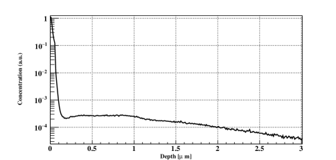
The wafer was uniformly doped with carbon in order to improve the irradiation hardness, and the doping concentration distribution is measured through Secondary Ion Mass Spectrometry (SIMS). Passivation SiO2 layers are removed before SIMS is performed. The SIMS result is shown in Figure 3. Considering carbon is injected before oxidation and surface passivation, carbon exists in the SiO2 and passivation layers, but the SIMS does not include these two layers.
3 Irradiation and Experiment Setups
3.1 Irradiation
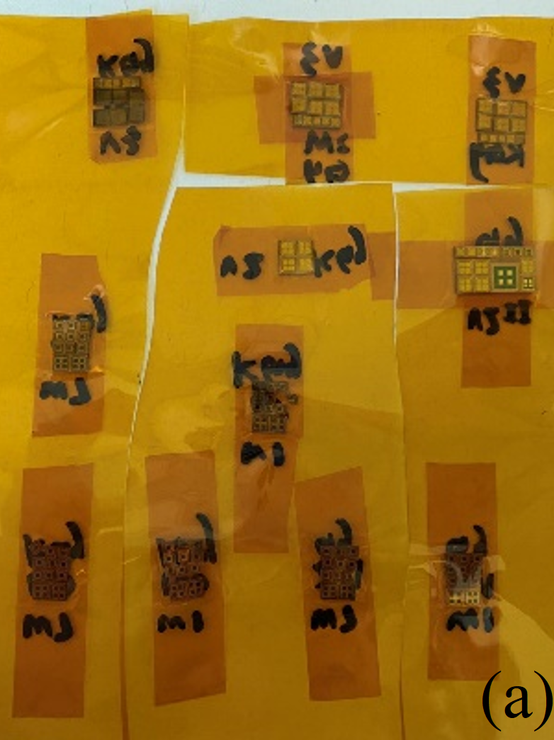
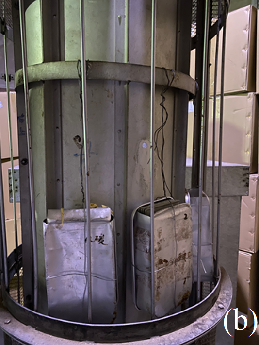
Irradiation test was carried out at the China Institute of Atomic Energy (CIAE). Samples are fixed using Kapton tapes, and placed in the aluminum boxes, around the cylindrical 60Co irradiation source, which causes damage in silicon sensors by Compton electrons and photoelectrons, as shown in Figure 4.
Irradiation dose rate is 1.0015% Gy/h ( 2.7715% Gy/s). The LGAD of all six types of IP was irradiated to three doses, namely 10k, 100k, and 2M Gy, as summarized in Table 1. Different doses of irradiation for the same IP of LGAD are obtained from different samples from the same wafer. Due to the small sample size compared to the diameter of the radiation source, the irradiation is uniform.
3.2 Experiment Setups
All tests, including IV, CV, and Inter-pad resistance, were conducted in the clean room of IHEP at a temperature of 20-22 ∘C and a humidity of 10-12%. The errors of the measuring apparatus are summarized in Table 2.
| Apparatus | Accuracy | Used in measurement |
|---|---|---|
| Keithley 2400 | 0.012% | IV CV Resistance |
| Keithley 2410 | 0.02% | IV Resistance |
| Keysight E4980A | 0.05% | CV |
The leakage currents are measured from A to A, and break-down current is defined as 1 A. Negative bias potential is applied to chuck in 2V increment for IV and inter-pad resistances, and in 0.5V increment for CV.
For IV and CV tests, one pad and guard ring are grounded, with the rest pads floating. For inter-pad resistance, three pads and the guard ring are connected by gold wires and grounded, as illustrated in Figure 2 (b). The rest pad (bias pad) is biased with a voltage range of -1 V to 1 V in 0.5 V increments. The leakage current is measured on ground pads and the bias current is measured on the biased pad.
Since different experiments require different wiring methods, the effects of different wiring methods with respect to the guard ring plus 0, 1, 2, and 3 pads floating are analyzed. No significant change in leakage current and BV are observed by changing the wiring method, and therefore the following experimental results can be excluded as a result of the test method.
4 Description and Analysis of Result
Results of Leakage Current versus Bias Voltage(I-V) and BV are shown in 4.1; inter-pad resistance is analyzed in 4.2; some other issues on bulk damages are discussed in 4.3.
4.1 Leakage Current versus Bias Voltage(I-V)
In general, an increase in both leakage current and BV after irradiation was observed. This conclusion holds for all IP. The following is the detailed analysis process.
I-V characteristics of IHEP-IME LGAD before and after irradiation are measured as shown in Figure 5, and take v3 2-5, 2-9, and v1 2-5 as examples.
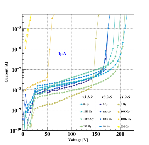
For v3 2-5, the leakage currents increase with the rise in irradiation dose, reaching three times the pre-irradiation value after exposure to 2 MGy of irradiation. The variation in breakdown voltage (BV) among different irradiation doses is approximately 5 V. Similarly, for v3 2-9, the trend of leakage currents before breakdown resembles that of sample v3 2-5, but BV increases by 20 V after being subjected to 2 MGy of irradiation. For v1 2-5, the leakage current is greater than that of v3, and BV is lower than v3 before irradiation. The BV of v1 decreases dramatically after irradiation, indicating that v1 is damaged. v3 samples have undergone a surface passivation process compared to v1, which may be responsible for the increased irradiation hardness but remains to be further investigated. V1 will not be studied in the following due to poor performance.
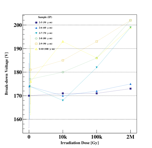
All samples are investigated in a similar way, and results are shown in Figure 6. BV increases with increasing irradiation dose, rising by 5 V-30 V for different samples after 2M Gy irradiation. This trend is particularly significant in samples 2-7, 2-8, 2-9, and 2-10, where the rise is greater than 20 V. Considering different doses of irradiation for the same IP of LGAD are obtained from different samples from the same wafer and the BV of the whole wafer has about 10% spread before irradiation, a change of 15V or more in BV after irradiation can be deemed to be caused by irradiation. Consequently, the observed BV rise in samples 2-7, 2-8, 2-9, and 2-10 can be attributed confidently to the irradiation effects. The variations observed in 2-5 and 2-6 are smaller than the 10% BV spread, and therefore the relationship between BV and irradiation dose cannot be determined in these cases.
4.2 Inter-pad Resistance versus Bias Voltage
Inter-pad resistance (R) refers to the resistance between electrodes, specifically the resistance between the grounded and biased pads. In operational LGADs, lateral currents can be generated between electrodes, leading to increased noise and reduced signal-to-noise ratio. A larger R-value helps to reduce these lateral currents. In this study, the R values of v3 samples 2-5, 2-6, 2-7, 2-8, 2-9, and 2-10 were measured.
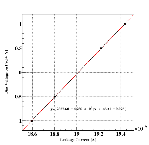
To calculate R, a plot of the bias voltage on the biased pad the leakage current is created, and a linear fit is applied to the slope of this I-V characteristic, yielding the resistance value. Figure 7 shows the I-V characteristic and its linear fit for v3 2-5 at a chuck bias of -85 V before irradiation. The plot demonstrates excellent linearity with an value greater than 0.99. It is worth noting that the current used to calculate R includes the current from both the substrate and neighbor pads. This can result in a lower calculated resistance value, and the actual resistance is higher than the calculated result.
For this study, the reference operating voltage is selected at 85 V. The R of all samples are shown in Figure 8. All samples, including those irradiated to 2 MGy, exhibit R values greater than , which is two orders of magnitude higher than the non-carbon-doped HPK LGAD irradiated to 2.5 MGy, where R decreases by four orders after irradiation [8]. HPK’s LGAD also features a passivation layer. For v3, no significant trends, such as shifts, increases, or decreases in R, were observed, indicating that irradiation did not have a significant impact on R. Since all samples have R values greater than , it can be concluded that the design of v3 meets the design requirements of having R values greater than 1 G.

4.3 Extra discussion –Capacitance (C-V) and related quantities
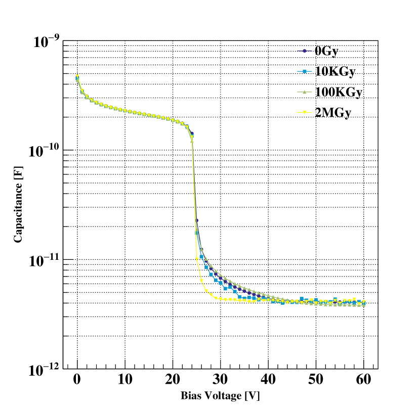
This section discusses the capacitance versus bias voltage (CV), Vgl, acceptor removal constant. The CVs of v3 2-5 with IP 50 m are shown in Figure 9. The figure shows the capacitance values are all less than 4.5 pF, no significant shape change is observed before and after 2M Gy irradiation, and all other samples show the same properties.
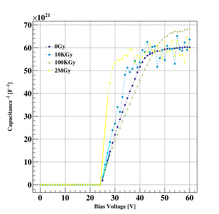
Another aspect studied is the gain layer depletion voltage (Vgl) and the acceptor removal constant, which characterize the bulk damage effect of irradiation.
Calculated Vgl is the intersection of the linear fitted line through three points after the turning point and the line y=0 in the -V curve.
Similarly, Vgl is calculated for the other samples and fitted to equation (4.1), where Vgl and V0,gl represent the gain layer depletion voltages before and after irradiation, is the total ionizing dose measured in Gy, and c is the acceptor removal constant measured in 1/Gy. The fitting results are presented in Figure 10, and the constants c are determined to be in the order of for all samples. It can be observed that there is no significant change in Vgl across different IP. This suggests that no bulk damage caused by gamma irradiation is observed.
| (4.1) |
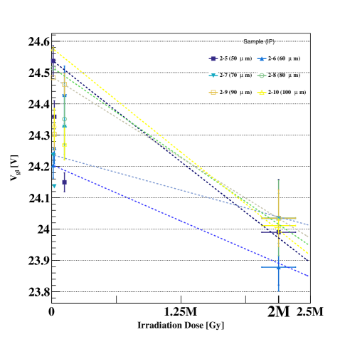
To summarize, except for the slight decrease in Vgl after irradiation, no significant effects of irradiation on other parameters are observed.
5 Conclusion
After 60Co irradiation, the surface components of LGADs were found to be affected, resulting in changes in the studied characteristic parameters. The effects of irradiation on LGADs can be summarized as follows:
-
•
An increase in leakage current by approximately half an order and a small increase in BV were observed after irradiation.
-
•
In the case of v3, no significant change in inter-pad resistance was observed before and after irradiation.
-
•
There was no correlation between the current used to calculate R parameters and inter-pad spacing, and no significant bulk damage was observed in all tests.
Based on these findings, it can be concluded that v3 demonstrates irradiation hardness indicators under the dose of 2M Gy in terms of BV(180-200 V), inter-pad resistance(> 1G), and capacitance(< 4.5 pF). These results indicate carbon doping combined with surface passivation increases radiation hardness. This study will contribute to the optimization of future LGAD surface designs of inter-pad distance, the gap between the active edge and the guard ring, and the maximum fill factor.
Acknowledgments
This work was supported in part by the National Natural Science Foundation of China under Grant 12105298, Grant 12275290 and Grant 12175252; in part by the State Key Laboratory of Particle Detection and Electronics under Grant No.SKLPDE-ZZ-202315.
References
- [1] Technical Proposal: A High-Granularity Timing Detector for the ATLAS Phase-II Upgrade. doi: 10.17181/CERN.CIUJ.KS4H.
- Apo [2015] High-Luminosity Large Hadron Collider (HL-LHC) : Preliminary Design Report. 12 2015. doi: 10.5170/CERN-2015-005.
- Aberle et al. [2020] O Aberle, E Carlier, E Barzi, G Ferlin, C Parente, E Skordis, K Einsweiler, S Atieh, A Patapenka, R Calaga, et al. submitter: High-luminosity large hadron collider (hl-lhc): Technical design report. Technical report, CERN, 2020.
- Bharthuar et al. [2021] Shudhashil Bharthuar, Jennifer Ott, Erik Brücken, Akiko Gädda, Stefanie Kirschenmann, Maria Golovleva, and Panja R Luukka. Effect of thermal donors induced in bulk and variation in p-stop dose on the no-gain region width measurements of lgads. In Proceedings of the 29th International Workshop on Vertex Detectors (VERTEX2020), page 010020. Journal of the Physical Society of Japan, jun 2021. doi: 10.7566/jpscp.34.010020.
- Cooke [2022] Charlotte Cooke. Upgrade of the cms barrel electromagnetic calorimeter for the high luminosity lhc. Instruments, 6(3), 2022. ISSN 2410-390X. doi: 10.3390/instruments6030029. URL https://www.mdpi.com/2410-390X/6/3/29.
- Ferrero et al. [2019] M. Ferrero, R. Arcidiacono, M. Barozzi, M. Boscardin, N. Cartiglia, G.F. Dalla Betta, Z. Galloway, M. Mandurrino, S. Mazza, G. Paternoster, F. Ficorella, L. Pancheri, H-F W. Sadrozinski, F. Siviero, V. Sola, A. Staiano, A. Seiden, M. Tornago, and Y. Zhao. Radiation resistant lgad design. Nucl. Instrum. Methods Phys. Res. A: Accel. Spectrom. Detect. Assoc. Equip., 919:16–26, 2019. ISSN 0168-9002. doi: https://doi.org/10.1016/j.nima.2018.11.121. URL https://www.sciencedirect.com/science/article/pii/S0168900218317741.
- Heller et al. [2022] R. Heller, C. Madrid, A. Apresyan, W.K. Brooks, W. Chen, G. D’Amen, G. Giacomini, I. Goya, K. Hara, S. Kita, S. Los, A. Molnar, K. Nakamura, C. Peña, C. San Martín, A. Tricoli, T. Ueda, and S. Xie. Characterization of bnl and hpk ac-lgad sensors with a 120 gev proton beam. J. Instrum., 17(05):P05001, may 2022. doi: 10.1088/1748-0221/17/05/P05001. URL https://dx.doi.org/10.1088/1748-0221/17/05/P05001.
- Hoeferkamp et al. [2022] Martin Hoeferkamp, Alissa Howard, Gregor Kramberger, Sally Seidel, Josef Sorenson, and Adam Yanez. Characterization of low gain avalanche detector prototypes’ response to gamma radiation. Front. Phys., page 105, 2022. doi: 10.3389/fphy.2022.838463.
- Lecoq [2020] P. Lecoq. Scintillation Detectors for Charged Particles and Photons, pages 45–89. Springer International Publishing, Cham, 2020. ISBN 978-3-030-35318-6. doi: 10.1007/978-3-030-35318-6_3. URL https://doi.org/10.1007/978-3-030-35318-6_3.
- Li et al. [2022] C.H. Li, X. Yang, J.J. Ge, T. Wang, X.X. Zheng, Y.J. Sun, and Y.W. Liu. Performance of lgad sensors with carbon enriched gain layer produced by ustc. Nucl. Instrum. Methods Phys. Res. A: Accel. Spectrom. Detect. Assoc. Equip., 1039:167008, 2022. ISSN 0168-9002. doi: https://doi.org/10.1016/j.nima.2022.167008. URL https://www.sciencedirect.com/science/article/pii/S0168900222004375.
- Mazini et al. [2021] Rachid Mazini, ATLAS Collaboration, et al. A high granularity timing detector for the atlas phase-ii upgrade. Technical report, ATL-COM-HGTD-2021-014, 2021. URL https://cds.cern.ch/record/2777584.
- Moffat et al. [2018] N. Moffat, R. Bates, M. Bullough, L. Flores, D. Maneuski, L. Simon, N. Tartoni, F. Doherty, and J. Ashby. Low gain avalanche detectors (lgad) for particle physics and synchrotron applications. J. Instrum., 13(03):C03014, mar 2018. doi: 10.1088/1748-0221/13/03/C03014. URL https://dx.doi.org/10.1088/1748-0221/13/03/C03014.
- Moll [2018] Michael Moll. Displacement damage in silicon detectors for high energy physics. IEEE Trans. Nucl. Sci., 65(8):1561–1582, 2018. doi: 10.1109/tns.2018.2819506.
- Tan et al. [2021] Yuhang Tan, Tao Yang, Suyu Xiao, Kewei Wu, Lei Wang, Yaoqian Li, Zhenwei Liu, Zhijun Liang, Dejun Han, Xingan Zhang, and Xin Shi. Radiation effects on ndl prototype lgad sensors after proton irradiation. Nucl. Instrum. Methods Phys. Res. A: Accel. Spectrom. Detect. Assoc. Equip., 1010:165559, 2021. ISSN 0168-9002. doi: https://doi.org/10.1016/j.nima.2021.165559. URL https://www.sciencedirect.com/science/article/pii/S0168900221005441.
- Yang et al. [2022] Tao Yang, Kewei Wu, Mei Zhao, Xuewei Jia, Yuhang Tan, Suyu Xiao, Kai Liu, Xiyuan Zhang, Congcong Wang, Mengzhao Li, Yunyun Fan, Shuqi Li, Chengjun Yu, Han Cui, Hao Zeng, Mingjie Zhai, Shuiting Xin, Maoqiang Jing, Gangping Yan, Qionghua Zhai, Mingzheng Ding, Gaobo Xu, Huaxiang Yin, Gregor Kramberger, Zhijun Liang, João Guimarães da Costa, and Xin Shi. Leakage current simulations of low gain avalanche diode with improved radiation damage modeling. Nucl. Instrum. Methods Phys. Res. A: Accel. Spectrom. Detect. Assoc. Equip., 1040:167111, 2022. ISSN 0168-9002. doi: https://doi.org/10.1016/j.nima.2022.167111. URL https://www.sciencedirect.com/science/article/pii/S0168900222005083.
- Zhang et al. [2012] J Zhang, E Fretwurst, R Klanner, I Pintilie, J Schwandt, and M Turcato. Investigation of x-ray induced radiation damage at the si-sio2 interface of silicon sensors for the european xfel. J. Instrum., 7(12):C12012, dec 2012. doi: 10.1088/1748-0221/7/12/C12012. URL https://dx.doi.org/10.1088/1748-0221/7/12/C12012.