The Role of Self-Torques in Transition Metal Dichalcogenide/Ferromagnet Bilayers
Abstract
In recent years, transition metal dichalcogenides (TMDs) have been extensively studied for their efficient spin-orbit torque generation in TMD/ferromagnetic bilayers, owing to their large spin-orbit coupling, large variety of crystal symmetries, and pristine interfaces. Although the TMD layer was considered essential for the generation of the observed SOTs, recent reports show the presence of a self-torque in single-layer ferromagnetic devices with magnitudes comparable to TMD/ferromagnetic devices. Here, we perform second-harmonic Hall SOT measurements on metal-organic chemical vapor deposition (MOCVD) grown MoS2/permalloy/Al2O3 devices and compare them to a single-layer permalloy/Al2O3 device to accurately disentangle the role of self-torques, arising from the ferromagnetic layer, from contributions from the TMD layer in these bilayers. We report a damping-like self-torque of in our single-layer permalloy/Al2O3 device, while we observe a weaker with opposite sign in one MoS2/permalloy/Al2O3 device, and no significant for all other MoS2/permalloy/Al2O3 devices. The opposite sign of these torques indicates a competition between the self-torque and the torque arising from the TMD layer, which would reduce the observed torque in these bilayers. In addition, we find a field-like spin-torque conductivity of in a single-layer permalloy/Al2O3 device, which is comparable to control MoS2/permalloy/Al2O3 devices and previous reports on similar TMD/FM bilayers, indicating only a minor role of the MoS2 layer. Finally, we find a linear dependence of the SOT conductivity on the Hall bar leg/channel width ratio of our devices, indicating that the Hall bar dimensions are of significant importance for the reported SOT strength. Our results accentuate the importance of delicate details, like device asymmetry, Hall bar dimensions, and self-torque generation, for the correct disentanglement of the microscopic origins underlying the SOTs, essential for future energy-efficient spintronic applications.
I Introduction
Manipulating the magnetization of a magnetic layer by means of a charge current holds an immense promise for more energy-efficient ways of storing and writing information [28, 29, 6]. By first converting a charge current into a spin current in materials with large spin-orbit coupling (SOC), the spin current can subsequently exert a torque on the magnetization of an interfaced magnetic material [29]. These current-induced torques, originating from the spin-orbit interaction, are referred to as spin-orbit torques (SOTs). To maximize the SOT strength, an efficient charge-to-spin conversion is advantageous, and thus, materials with large spin-orbit coupling (Pt [8, 7, 32], Pd [15, 9, 21], W [34, 5], Ta [23, 4, 18], Hf [45, 1, 35], etc.) have been extensively studied [44]. Two main mechanisms for the charge-to-spin conversion in these materials are the spin-Hall (SHE) and the Rashba-Edelstein effect (REE) [29, 38]. For these polycrystalline spin Hall metals with inversion symmetry, these effects, however, do not possess the ideal symmetry for field-free switching of the magnetization of magnetic layers with perpendicular magnetic anisotropy (PMA) used in modern high-density memory storage [49, 24]. Therefore, other materials such as topological insulators and two-dimensional (2D) van der Waals crystals have been employed to search for new materials which do allow for field-free switching [41, 38, 19, 48, 20].
In this regard, the family of 2D van der Waals materials called the transition metal dichalcogenides (TMDs) have gained much interest as spin source material, owing to their large SOC, atomically-flat surfaces and broad range of crystal symmetries [12, 14, 24]. The more conventional and well known semiconducting TMDs, such as WSe2 [13, 39, 33], WS2 [25], MoS2 [39, 50], were studied first, due to their air stability and developed wafer-scale growth. More recently, however, the low symmetry TMDs have gained much interest since the observation of the out-of-plane damping-like torque in TMD/FM bilayers, which is optimal for switching magnets with PMA [26, 27, 10, 42, 43, 40, 17].
Previous reports on SOTs in TMD/ferromagnetic (FM) bilayers often consider the TMD as essential for the generation of the observed SOTs, either through bulk effects, such as the spin-Hall effect, or effects arising from the TMD/Py interface, such as the Rashba-Edelstein effect, spin-orbit filtering or spin-orbit precession [2, 46]. More recent reports, however, indicate the presence of a self-torque in single-layer ferromagnetic devices without the presence of a spin source material. A recent study performed magneto-optic Kerr effect (MOKE) measurements to probe the SOT at the surface of a single-layer Py device and observe a sizable SOT at the Py interface, which is ascribed to a SHE in the Py [47]. Also, electrical measurements on Py capped with SiO2 or Al2O3 show the presence of field-like and damping-like torques in Py devices [37]. And in metallic bilayers, it was shown that self-induced torques lead to errors in the estimation of the spin-torque strength [3]. These self-torques in ferromagnetic materials make it difficult to accurately determine to what extent the TMD layer is contributing to the SOT [37].
Here, we report second-harmonic Hall measurements on MoS2/Py/Al2O3 and single-layer Py/Al2O3 devices to disentangle the contribution of self-torques from the FM layer, and more accurately determine the effect of the MoS2 layer. We find that the damping-like self-torque in a Py/Al2O3 device is of opposite sign to the damping-like torque found in one of our MoS2/Py/Al2O3 devices, indicating a competition between the two. Furthermore, we show that the field-like self-torque in a single-layer Py/Al2O3 device can be of similar magnitude compared to MoS2/Py/Al2O3 devices, indicating a minor effect of the TMD. In addition, we study the dependence of the spin-orbit torque on the contact/channel width ratio and find a linear dependence of the field-like spin-torque conductivity on the channel width. These results indicate the importance of single-layer reference samples and the device specifics for an accurate determination of the microscopic mechanisms underlying the spin-orbit torques.
II Results and Discussion
II.1 MoS2/Py/Al2O3 devices
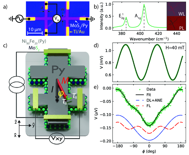
We use wafer-scale grown MoS2 obtained by metal-organic chemical vapor deposition (MOCVD) [16]. The MOCVD grown MoS2 layer is characterized using photoluminescence (PL) microscopy and Raman spectroscopy (see Fig. 1(b)) before device fabrication. The two characteristic bands of monolayer MoS2 at 385 cm-1 and 405 cm-1, corresponding to the in-plane () and out-of-plane phonon mode (), respectively, are clearly observed, as indicated in Fig. 1b [22]. Furthermore, a strong and homogeneous PL is obtained using PL microscopy shown in the insets of Fig. 1(b), indicating the homogeneous coverage of monolayer MoS2 with little strain on the substrate.
Next, multiple MoS2/Py/Al2O3 Hall bar devices with different channel width (w)/leg width (a) ratios (Fig. 1a) were fabricated to perform the harmonic Hall measurements. Here, the first () and second () harmonic Hall voltage are measured while an applied magnetic field () is rotated in-plane, making an angle with respect to the current direction (Fig. 1(c), details are described in the Methods section). When assuming a small magnetic anisotropy compared to , the magnetization is aligned with the external magnetic field and the first-harmonic Hall voltage () is given by [8, 11, 31]:
| (1) |
where is the magnetic field’s polar angle ( for in-plane measurements) and the and are the planar Hall and anomalous Hall effect resistance, respectively. The first-harmonic Hall voltage (), depicted in Fig. 1(d) for a magnetic field of 40 mT, nicely follows a behavior due to the planar Hall effect of the Py layer. By fitting the data to Eq.(1) we extract a planar Hall resistance of . In previous reports on exfoliated TMD/FM bilayers, large deviations from the dependence were observed at low magnetic fields, indicating that a strong uniaxial magnetic anisotropy was induced in the Py [13, 26, 43, 42]. In these reports, the induced anisotropy was attributed to a strong interaction between the Py and the crystalline structure of the underlying TMD. As the MOCVD grown TMD in our devices has a grain size of around 1 m, our Hall bar covers multiple domains. Therefore, no induced magnetic anisotropy in the Py from the TMD crystal structure is expected. This is in line with our observation, as only minor deviations from the fit are observed. For devices with a larger Hall bar channel width/leg width ratio, these minor deviations disappear completely, indicating that the minor deviations observed for narrow Hall bars are likely due to shape anisotropy of the Hall bar.
To determine the field-like () and damping-like torques (), the second-harmonic Hall (SHH) voltage is measured (Fig. 1(e)). The second-harmonic Hall voltage can be described by [8, 11]:
| (2) |
where the A- and B-components are given by:
| (3) |
| (4) |
Here, is the gyromagnetic ratio, is the out-of-plane anisotropy field, and is the anomalous Nernst resistance. The SHH is fitted using Eq.(2) to extract the amplitude of the and components, referred to as the A- and B-components, respectively. As can be seen from Fig. 1(e), our data is well described by Eq.(2). Subsequently, the A- and B-components are determined for different magnetic fields, allowing us to extract the , and anomalous Nernst resistance () using Eq.(3) and Eq.(4). For the MoS2/Py/Al2O3 devices, we corrected our data for a systematic 15 mT offset in the field. The is obtained by performing a separate measurement where the first harmonic Hall voltage is measured while sweeping the magnetic field out-of-plane from approximately -1 T to 1 T.
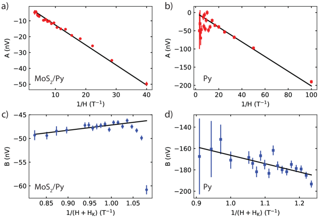
Figure 2(a) and (c) show the field-dependence of the A- and B-component of a MOCVD MoS2/Py/Al2O3 device, respectively. As expected from Eq.(3), the A-component shows a linear dependence on the inverse magnetic field, which clearly indicates the presence of a field-like torque . Using Eq.(3) we find a ranging from T to T, for an applied current density of 0.8 A/m2 to 5 A/m2. This corresponds to a spin-torque conductivity of to , respectively (see the Methods section for the spin-torque conductivity calculation). This value is comparable to previous reports on chemical vapor deposition (CVD) grown MoS2/CoFeB devices from Shao et al. [39] and slightly lower compared to other semiconducting TMD/Py devices (e.g. WS2, WSe2) [39, 25, 13, 33]. Larger field-like torques are reported in semimetallic TMD/Py bilayers, which is explained by the considerable Oersted torque arising from the current flowing through the conducting TMD [26, 10, 42]. Due to the semiconducting character of the MoS2 layer in our devices, no current is expected to flow through the MoS2 and thus no Oersted torque is expected.
The field dependence of the B-component is depicted in Fig. 2(c). In the presence of a , a linear dependence is expected versus the inverse field (see Eq.(4), similar to the A-component). At low magnetic fields, however, we observe large deviations from the linear dependence. This can be explained by the fact that Eq.(3) and Eq.(4) are derived assuming that , where is the in-plane uniaxial anisotropy field, which does not hold anymore at low magnetic fields [11]. To get a more accurate estimate of the damping-like torque, we therefore neglect the three data point at lowest field when fitting the data to Eq.(4). For the majority of our devices, we find a with a large error, ranging from T to T, corresponding to a spin-torque conductivity ranging from to . Due to the large errors, we cannot conclude that these devices show a significant damping-like torque. For one of the samples, however, we find a damping-like torque with a smaller error T, corresponding to . This value is comparable to values reported in SOT devices made with Pt, W, and NiPS3, and are significantly higher compared to SOT devices using more conventional TMDs (e.g. WTe2, MoTe2, WSe2, etc.). The presence of both a field-like and damping-like torque in MoS2/Py has been previously reported by Zhang et al. in ST-FMR measurements [50]. There, a torque ratio of is reported, indicating a 5 times stronger damping-like torque. Similarly, we find a stronger damping-like torque for this one device, showing a damping-like torque a factor of 20 stronger than the field-like torque. On the other hand, Shao et al. report no damping-like torque in their SHH measurements on MoS2/CoFeB bilayers [39], similar to our other devices. These contrasting observations show that there is a significant device-to-device variation for the damping-like torque in these bilayers.
II.2 Single-layer Py/Al2O3 device
To determine the contribution of possible self-torques in the Py-layer and accurately resolve the effect of the MOCVD grown MoS2 layer on the SOTs, we compare the SOTs measurements from the MoS2/Py/Al2O3 device to a single-layer Py/Al2O3 reference device. In Fig. 2(b) and (d) the extracted A- and B-components for the single-layer Py/Al2O3 device are plotted versus the inverse field. Surprisingly, even without the MoS2 layer, we observe a clear linear dependence for the A-component similar to the MoS2/Py/Al2O3 devices, indicating the presence of a field-like self-torque. Using Eq.(3) and Eq.(5), we find T and . The has the same sign and its magnitude is only lower compared to the MoS2/Py/Al2O3 device, which indicates that the presence of the TMD layer does not significantly enhance the field-like SOT conductivity.
For the B-component, however, no large deviations at low fields are observed, as was the case with the MoS2/Py/Al2O3 device. Using Eq.(3) and Eq.(5), we find T and for the damping-like torque, which is larger and has an opposite sign compared to the MoS2/Py/Al2O3 device that did show a significant damping-like torque. For the MoS2/Py/Al2O3 devices, the self-torque from the Py and the torque arising from the TMD/Py interaction might both be present. As these torques have opposite sign, their competition reduces the net damping-like torque, which could explain the absence of a damping-like torque in the majority of our MoS2/Py/Al2O3 devices. This suggests that the addition of the TMD layer causes a suppression of the rather than an increase, as was reported by Zhang et al. [50] in CVD grown MoS2/Py devices. Furthermore, differences in the interface quality, resulting in different contributions of the self-torque in Py and the torque arising from the TMD/FM interface could explain the contrasting SOT observations in MoS2/CoFeB and MoS2/Py devices [39, 50].
Other reports on single-layer Py devices show both a damping-like and a field-like torque in ST-FMR measurements [37]. Although a field-like torque was observed in all devices, only a damping-like torque was observed in devices where the structural inversion symmetry was broken. In our devices, the structural inversion symmetry is broken as well, as the Py is evaporated on SiO2 and capped with Al2O3, and thus possesses two different interfaces. A difference in electron-scattering from these two interfaces could, in turn, lead to a self-torque. Furthermore, Seki et al. report only damping-like torques for devices where the Py layer is sufficiently thin ( nm), which is in contrast to our observation, as we observe a rather strong damping-like torque with a Py thickness of 6 nm [37]. Also, Schippers et al. report measurements on a similar single-layer Py reference sample with a 6 nm Py thickness, capped with Al2O3 [36]. At room temperature, they find a which is 3 times larger, and a which is one order of magnitude smaller. For their samples, however, the layers are deposited using magnetron sputtering, while our samples employed electron beam evaporation, which could lead to different material and interface qualities, and different current distributions in the Py layer.
All these different torque strengths and directions observed for similar MoS2/FM bilayers and single-layer Py devices underline the large device-to-device variation, also observed in our devices. Our observations show that the self-torque, originating solely from the FM layer, can have a significant contribution to the observed SOTs in TMD/FM bilayers.
II.3 Effect of the Hall bar dimensions
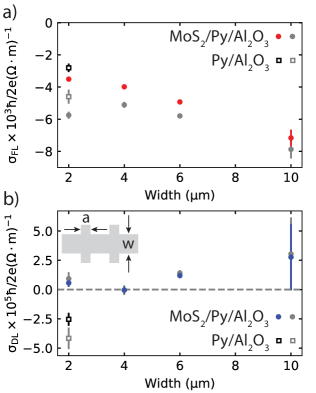
Lastly, we study the effect of the Hall bar leg width/channel width ratio for the MoS2/Py/Al2O3 devices by keeping the leg width constant at 2 m, while varying the channel width () from 2 m to 10 m, plotted in Fig. 3. The extracted field-like (red circles) and damping-like spin-torque conductivities (blue circle) for all devices are plotted versus the channel width in Fig. 3(a) and (b), respectively. The from the single-layer Py/Al2O3 device are included and depicted by the black unfilled squares for comparison. We observe a clear, almost linear, dependence of on the channel width. The for the 10 m device is a factor 2 larger than the 2 m device. We stress that the larger error bar for the device with a channel width of 10 m is ascribed to a smaller current density compared to the other devices. This observation is in line with recent work from Neumann et al. where the leg width/channel width ratio is shown to affect the estimation of the spin-Hall angle () [30]. A significantly decreasing is found when the leg width/channel width ratio becomes sufficiently big (), reporting a value of only at a leg width/channel width ratio of 1. To correct our , we incorporate a factor for each leg width/channel width ratio as reported by Neumann et al. [30], shown in Fig. 3 as gray circles.
After the correction, there is no clear monotonic decrease of with the leg width/channel width ratio. However, still some device-to-device variation is found, which could be due to varying interface and material qualities. For , the reported values for both the MoS2/Py/Al2O3 and the single-layer Py/Al2O3 devices remain large with correspondingly large error bars as previously discussed.
III Conclusion
In conclusion, our results indicate that the self-torques, originating from the FM layer, can have significant contributions to the observed SOTs in TMD/FM bilayers. We find a significant in our Py/Al2O3 reference device with an opposite sign compared to the found in a MoS2/Py/Al2O3 device. These findings suggest that the self-torque from the FM layer can compete with torques originating from the presence of the TMD layer, reducing the torque strength in TMD/FM bilayers. In addition, we observe a similar in single-layer Py/Al2O3 devices, indicating that the MOCVD MoS2 layer in our MoS2/Py/Al2O3 is of minor importance for the generation of a field-like SOTs. Both findings suggest that the FM layer, rather than the TMD, might play a dominant role in the generation of the observed SOTs in TMD/FM bilayers. Previous contrasting SOT observations in similar TMD/FM bilayers could thus be ascribed to differences in the FM layer (e.g., different fabrication techniques, capping layers, interface quality, etc.) rather than different interactions between the TMD and the FM. We therefore recommend that the self-torque in a single-layer FM reference samples are also characterized in future studies in order to accurately determine the effect of the TMD layer on the observed SOTs, and that the Hall bar dimensions should be clearly reported. In addition, in HM/FM bilayers, the self-torque in the FM layers could counteract the torque generated by the HM layer, resulting in a reduced net torque. Taking advantage of the self-torques in the FM layer, making them work in conjunction with other SOTs instead, could lead to an increase in the SOT efficiency [3]. Tailoring the FM interfaces to change the self-torque direction and strength, in conjunction with searching for different materials as SOT sources, could be a promising route towards an increase in SOT efficiency. These results pave the way for a more accurate disentanglement of all microscopic mechanisms at play, increasing our understanding of the origins underlying the SOTs, which is essential for more energy efficient magnetic memory devices.
IV Methods
IV.1 Device fabrication
The MoS2 layer was grown using metal-organic chemical vapor deposition (MOCVD) on a SiO2/Si substrate as described in ref[16]. The MoS2 is characterized with a PL microscope using a BrightLine long-pass filter set to check the homogeneity of the monolayer coverage on the SiO2/Si substrate (see Fig. 1).
Next, a prepared PMMA mask with exposed Hall bars of different widths is deposited on top of the MoS2 covered substrate, which ensures a pristine interface between the permalloy and MoS2 with no polymer contamination. Using electron beam evaporation, 6 nm of permalloy and a capping layer and hard mask of 17 nm of Al2O3 are deposited. Subsequently, the contacts are defined using standard e-beam lithography techniques. Then, first an Al2O3 wet etch with tetramethylammonium is performed for 45 seconds at 40 ∘C, after which in-situ Ar-milling is performed prior to the evaporation of the Ti/Au (5/55 nm) contacts. Finally, the remaining MoS2 layer is removed using reactive ion etching (30 W RF, 5W ICP).
IV.2 Electrical measurements
The harmonic Hall measurements, illustrated in Fig. 1a and Fig. 1c, were performed at room temperature using a standard lock-in technique with low frequency (77.77 Hz) AC-currents (), ranging from A to A [8, 11, 31]. Subsequently, the first () and second () harmonic Hall voltage were measured while an applied magnetic field (), ranging from 10 mT to 300 mT, was rotated in-plane, making an angle with respect to the current (Fig. 1(c)).
To better compare the SOTs in our devices to previous reports on SOTs in TMD/FM bilayers, we express the SOT in terms of spin-torque conductivity; the common figure-of-merit in literature due to its independence on geometric factors [32, 42]. The spin-torque conductivity is defined as the total angular momentum absorbed by the ferromagnet per second, per unit interface area, per applied electric field, in units of , and is calculated according to:
| (5) |
where is the saturation magnetization, is the reduced Planks constant, is the electron charge, is the electric field, is the square resistance, is the applied current, and , , and are the length, width and Py thickness, respectively.
IV.3 Anomalous Hall measurement
To determine the anomalous Hall resistance, , and the saturation magnetization, , needed for determining the damping-like torque using Eq.4, we performed anomalous Hall measurements (Fig. 4). Using a standard lock-in technique with a low frequency (17.77 Hz) current of 1 µA, the Hall voltage is measured while an out-of-plane magnetic field is sweeped from -1 T to 1 T, as shown in Fig. 4. To reduce errors from any misalignment, the Hall voltage is antisymmetrized.

V Acknowledgements
We would like to acknowledge Prof. M. A. Loi and E. K. Tekelenburg for their help with the Raman measurements and thank J. G. Holstein, H. Adema, H. de Vries, A. Joshua, and F. H. van der Velde for their technical support. Sample fabrication was performed using NanoLabNL facilities. This work was supported by the Dutch Research Council (NWO—STU.019.014), the Zernike Institute for Advanced Materials, and innovation program under grant agreement No. 881603 (Graphene Flagship).
VI Author contributions
J.H. and K.M. fabricated the samples, and performed both the electrical and optical measurements under supervision of M.H.D.G.. F.M. and C.L. grew the MOCVD MoS2 layer under supervision of J.P. J.H. performed the data analysis under supervision of M.H.D.G. J.H. and M.H.D.G. wrote the paper with comments from all authors.
References
- Akyol et al. [2016] Akyol, M., Jiang, W., Yu, G., Fan, Y., Gunes, M., Ekicibil, A., Khalili Amiri, P., and Wang, K. L., Applied Physics Letters 109, 022403 (2016).
- Amin, Haney, and Stiles [2020] Amin, V. P., Haney, P. M., and Stiles, M. D., Journal of Applied Physics 128 (2020), 10.1063/5.0024019, arXiv:2008.01182 .
- Aoki et al. [2022] Aoki, M., Shigematsu, E., Ohshima, R., Shinjo, T., Shiraishi, M., and Ando, Y., Physical Review B 106, 174418 (2022).
- Avci et al. [2014] Avci, C. O., Garello, K., Gabureac, M., Ghosh, A., Fuhrer, A., Alvarado, S. F., and Gambardella, P., Physical Review B 90, 224427 (2014), arXiv:1412.0865 .
- Demasius et al. [2016] Demasius, K.-u., Phung, T., Zhang, W., Hughes, B. P., Yang, S.-H., Kellock, A., Han, W., Pushp, A., and Parkin, S. S. P., Nature Communications 7, 10644 (2016).
- Dieny et al. [2020] Dieny, B., Prejbeanu, I. L., Garello, K., Gambardella, P., Freitas, P., Lehndorff, R., Raberg, W., Ebels, U., Demokritov, S. O., Akerman, J., Deac, A., Pirro, P., Adelmann, C., Anane, A., Chumak, A. V., Hirohata, A., Mangin, S., Valenzuela, S. O., Onbaşlı, M. C., D’Aquino, M., Prenat, G., Finocchio, G., Lopez-Diaz, L., Chantrell, R., Chubykalo-Fesenko, O., and Bortolotti, P., Nature Electronics 3, 446 (2020).
- Fan et al. [2014] Fan, X., Celik, H., Wu, J., Ni, C., Lee, K.-J., Lorenz, V. O., and Xiao, J. Q., Nature Communications 5, 3042 (2014).
- Garello et al. [2013] Garello, K., Miron, I. M., Avci, C. O., Freimuth, F., Mokrousov, Y., Blügel, S., Auffret, S., Boulle, O., Gaudin, G., and Gambardella, P., Nature Nanotechnology 8, 587 (2013).
- Ghosh et al. [2017] Ghosh, A., Garello, K., Avci, C. O., Gabureac, M., and Gambardella, P., Physical Review Applied 7, 014004 (2017), arXiv:1701.01843 .
- Guimarães et al. [2018] Guimarães, M. H. D., Stiehl, G. M., MacNeill, D., Reynolds, N. D., and Ralph, D. C., Nano Letters 18, 1311 (2018), arXiv:1801.07281 .
- Hayashi et al. [2014] Hayashi, M., Kim, J., Yamanouchi, M., and Ohno, H., Physical Review B 89, 144425 (2014).
- Hidding and Guimarães [2020] Hidding, J. and Guimarães, M. H., Frontiers in Materials 7 (2020), 10.3389/fmats.2020.594771.
- Hidding et al. [2021] Hidding, J., Tirion, S. H., Momand, J., Kaverzin, A., Mostovoy, M., van Wees, B. J., Kooi, B. J., and Guimarães, M. H., JPhys Materials 4 (2021), 10.1088/2515-7639/ac24ee.
- Husain et al. [2020] Husain, S., Gupta, R., Kumar, A., Kumar, P., Behera, N., Brucas, R., Chaudhary, S., and Svedlindh, P., Applied Physics Reviews 7 (2020), 10.1063/5.0025318.
- Jamali et al. [2013] Jamali, M., Narayanapillai, K., Qiu, X., Loong, L. M., Manchon, A., and Yang, H., Physical Review Letters 111, 246602 (2013).
- Kang et al. [2015] Kang, K., Xie, S., Huang, L., Han, Y., Huang, P. Y., Mak, K. F., Kim, C.-j., and Muller, D., Nature 520, 656 (2015).
- Kao et al. [2022] Kao, I. H., Muzzio, R., Zhang, H., Zhu, M., Gobbo, J., Yuan, S., Weber, D., Rao, R., Li, J., Edgar, J. H., Goldberger, J. E., Yan, J., Mandrus, D. G., Hwang, J., Cheng, R., Katoch, J., and Singh, S., Nature Materials 21, 1029 (2022), arXiv:2012.12388 .
- Kim et al. [2013] Kim, J., Sinha, J., Hayashi, M., Yamanouchi, M., Fukami, S., Suzuki, T., Mitani, S., and Ohno, H., Nature Materials 12, 240 (2013).
- Krizakova et al. [2022] Krizakova, V., Perumkunnil, M., Couet, S., Gambardella, P., and Garello, K., Journal of Magnetism and Magnetic Materials 562, 169692 (2022).
- Kurebayashi et al. [2022] Kurebayashi, H., Garcia, J. H., Khan, S., Sinova, J., and Roche, S., Nature Reviews Physics 4, 150 (2022), arXiv:2107.03763 .
- Lee et al. [2014] Lee, H.-R., Lee, K., Cho, J., Choi, Y.-H., You, C.-Y., Jung, M.-H., Bonell, F., Shiota, Y., Miwa, S., and Suzuki, Y., Scientific Reports 4, 6548 (2014).
- Li et al. [2012] Li, H., Zhang, Q., Yap, C. C. R., Tay, B. K., Edwin, T. H. T., Olivier, A., and Baillargeat, D., Advanced Functional Materials 22, 1385 (2012).
- Liu et al. [2012] Liu, L., Pai, C.-F., Li, Y., Tseng, H. W., Ralph, D. C., and Buhrman, R. a., Science 336, 555 (2012), arXiv:1203.2875 .
- Liu and Shao [2020] Liu, Y. and Shao, Q., ACS Nano 14, 9389 (2020), arXiv:2003.11966 .
- Lv et al. [2018] Lv, W., Jia, Z., Wang, B., Lu, Y., Luo, X., Zhang, B., Zeng, Z., and Liu, Z., ACS Applied Materials and Interfaces 10, 2843 (2018).
- MacNeill et al. [2017a] MacNeill, D., Stiehl, G. M., Guimaraes, M. H., Buhrman, R. A., Park, J., and Ralph, D. C., Nature Physics 13, 300 (2017a), arXiv:1605.02712 .
- MacNeill et al. [2017b] MacNeill, D., Stiehl, G. M., Guimarães, M. H. D., Reynolds, N. D., Buhrman, R. A., and Ralph, D. C., Physical Review B 96, 054450 (2017b), arXiv:1707.03757 .
- Manchon et al. [2015] Manchon, A., Koo, H. C., Nitta, J., Frolov, S. M., and Duine, R. A., Nature Materials 14, 871 (2015), arXiv:1507.02408 .
- Manchon et al. [2019] Manchon, A., Železný, J., Miron, I. M., Jungwirth, T., Sinova, J., Thiaville, A., Garello, K., and Gambardella, P., Reviews of Modern Physics 91, 035004 (2019), arXiv:1801.09636 .
- Neumann and Meinert [2018] Neumann, L. and Meinert, M., AIP Advances 8, 095320 (2018), arXiv:1804.07577 .
- Nguyen and Pai [2021] Nguyen, M. H. and Pai, C. F., APL Materials 9 (2021), 10.1063/5.0041123.
- Nguyen, Ralph, and Buhrman [2016] Nguyen, M.-h., Ralph, D. C., and Buhrman, R. A., Physical Review Letters 116, 126601 (2016).
- Novakov et al. [2021] Novakov, S., Jariwala, B., Vu, N. M., Kozhakhmetov, A., Robinson, J. A., and Heron, J. T., ACS Applied Materials & Interfaces 13, 13744 (2021).
- Pai et al. [2012] Pai, C.-F., Liu, L., Li, Y., Tseng, H. W., Ralph, D. C., and Buhrman, R. A., Applied Physics Letters 101, 122404 (2012).
- Ramaswamy et al. [2016] Ramaswamy, R., Qiu, X., Dutta, T., Pollard, S. D., and Yang, H., Applied Physics Letters 108, 202406 (2016).
- Schippers, Swagten, and Guimarães [2020] Schippers, C. F., Swagten, H. J. M., and Guimarães, M. H. D., Physical Review Materials 4, 084007 (2020).
- Seki et al. [2021] Seki, T., Lau, Y.-C., Iihama, S., and Takanashi, K., Physical Review B 104, 094430 (2021).
- Shao et al. [2021] Shao, Q., Li, P., Liu, L., Yang, H., Fukami, S., Razavi, A., Wu, H., Wang, K., Freimuth, F., Mokrousov, Y., Stiles, M. D., Emori, S., Hoffmann, A., Akerman, J., Roy, K., Wang, J.-P., Yang, S.-H., Garello, K., and Zhang, W., IEEE Transactions on Magnetics 57, 1 (2021).
- Shao et al. [2016] Shao, Q., Yu, G., Lan, Y.-W. W., Shi, Y., Li, M.-Y. Y., Zheng, C., Zhu, X., Li, L.-J. J., Amiri, P. K., and Wang, K. L., Nano Letters 16, 75147520 (2016).
- Shi et al. [2019] Shi, S., Liang, S., Zhu, Z., Cai, K., Pollard, S. D., Wang, Y., Wang, J., Wang, Q., He, P., Yu, J., Eda, G., Liang, G., and Yang, H., Nature Nanotechnology 14, 945 (2019).
- Sousa, Tatara, and Ferreira [2020] Sousa, F., Tatara, G., and Ferreira, A., Physical Review Research 2, 043401 (2020), arXiv:2005.09670 .
- Stiehl et al. [2019a] Stiehl, G. M., Li, R., Gupta, V., Baggari, I. E., Jiang, S., Xie, H., Kourkoutis, L. F., Mak, K. F., Shan, J., Buhrman, R. A., and Ralph, D. C., Physical Review B 100, 184402 (2019a), arXiv:1906.01068 .
- Stiehl et al. [2019b] Stiehl, G. M., MacNeill, D., Sivadas, N., El Baggari, I., Guimarães, M. H., Reynolds, N. D., Kourkoutis, L. F., Fennie, C. J., Buhrman, R. A., and Ralph, D. C., ACS Nano 13, 2599 (2019b), arXiv:1901.08908 .
- Tanaka et al. [2008] Tanaka, T., Kontani, H., Naito, M., Naito, T., Hirashima, D. S., Yamada, K., and Inoue, J., Physical Review B 77, 165117 (2008), arXiv:0711.1263 .
- Torrejon et al. [2014] Torrejon, J., Kim, J., Sinha, J., Mitani, S., Hayashi, M., Yamanouchi, M., and Ohno, H., Nature Communications 5, 4655 (2014).
- Veneri, Perkins, and Ferreira [2022] Veneri, A., Perkins, D. T. S., and Ferreira, A., Physical Review B 106, 235419 (2022), arXiv:2208.07296 .
- Wang et al. [2019] Wang, W., Wang, T., Amin, V. P., Wang, Y., Radhakrishnan, A., Davidson, A., Allen, S. R., Silva, T. J., Ohldag, H., Balzar, D., Zink, B. L., Haney, P. M., Xiao, J. Q., Cahill, D. G., Lorenz, V. O., and Fan, X., Nature Nanotechnology 14, 819 (2019).
- Yang et al. [2022] Yang, H., Valenzuela, S. O., Chshiev, M., Couet, S., Dieny, B., Dlubak, B., Fert, A., Garello, K., Jamet, M., Jeong, D.-E., Lee, K., Lee, T., Martin, M.-B., Kar, G. S., Sénéor, P., Shin, H.-J., and Roche, S., Nature 606, 663 (2022).
- Yu et al. [2014] Yu, G., Upadhyaya, P., Fan, Y., Alzate, J. G., Jiang, W., Wong, K. L., Takei, S., Bender, S. A., Chang, L. T., Jiang, Y., Lang, M., Tang, J., Wang, Y., Tserkovnyak, Y., Amiri, P. K., and Wang, K. L., Nature Nanotechnology 9, 548 (2014).
- Zhang et al. [2016] Zhang, W., Sklenar, J., Hsu, B., Jiang, W., Jungfleisch, M. B., Xiao, J., Fradin, F. Y., Liu, Y., Pearson, J. E., Ketterson, J. B., Yang, Z., and Hoffmann, A., APL Materials 4 (2016), 10.1063/1.4943076.