A Dual Threshold Analogue Content Addressable Memory
Abstract
Advances in machine learning and neuromorphic systems are fuelled by the development of architectures required for these applications, such as content addressable memory. In an attempt to address this need, this paper presents a new RRAM tuned window comparator, building upon existing work in reconfigurable computing. The circuit uses a low component count at 6T2R2M, comparable with the most compact existing cells of this type. This paper will present this design, demonstrating its operation with TiOx memristive devices, showing its controllability and specificity. This paper will then simulate the energy dissipated in its operation, showing it to be below per test, comparable to existing works.
Index Terms:
Associative memory, content addressable memory, RRAM, memristorI Introduction
Content addressable memory (CAM) is a broad term describing memory technologies where the memory cells compare their stored state with an input locally. This allows a bank of CAM to be quickly searched by applying the information that is being sought to the input of the array and monitoring the cell outputs. The combining of low level computing tasks with memory blurs the boundary between the two and could allow for advances in conventional computing[1], but has further potential in machine learning applications. CAM can serve as the foundation of the design of artificial neural nets and other neuromorphic systems[2].
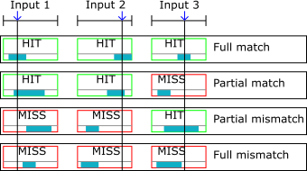
Content addressable memory technologies can be divided into two types: binary CAM and analogue CAM. Binary CAM stores only a high or low value, and usually compare this stored value with a binary input[3]. CMOS SRAM based CAM cells commonly find use in network switches, where they are used to store easily searchable tables of MAC address for faster signal routing[4]. In some cases, CAM can have a third stored state for ’don’t care’; this is called ternary CAM[5][6]. While CMOS binary CAM is well established, there is ongoing research in the area, trying to integrate novel nonvolatile memory elements such as RRAM[7]. Analogue CAM can have a range of different implementations, but often takes the form of a window comparator. In addition to their use in neuromorphic systems[8], this type of CAM can also be used in analogue signal analysis methods such as template matching[9]. Unlike binary CAM research, where the goal is to add nonvolatility to the cells without increasing power dissipation, analogue CAM research seeks to replace high power dissipation and area comparators with simplified circuits that take advantage of the analogue nature of emerging memory technologies. While there are more attempts to use FeRAM[10][11][12] for this purpose, an alternative memory for this application is RRAM[13][14], due to the granularity of states in RRAM technologies and the ease of controlling circuits with resistive elements. This works seeks to build upon existing work in reconfigurable computing[15], with the aim of producing a circuit closer in operation to the work of Can Li et al.[16]. This paper will demonstrate the validity of resistive models of the circuit under consideration, and then assess an integrated implementation of the design for the purpose of proving the concept and comparison with existing work.
II Circuit Design
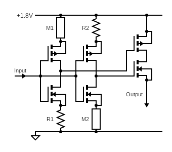
The circuit considered (Fig. 2) is based upon a skewed inverter design. Two complementary FET pairs with source degeneration are used as the input stage with their outputs assessed by an XOR mode transmission gate. The ratio between source degeneration on the input PMOS and NMOS alters the threshold of the inverter. As the threshold is dependent on the ratio between the top and bottom degeneration resistors and not the total resistance of the branch, the threshold can be controlled by altering the state of only one of them. As such, this design uses a single dynamic RRAM device to control each threshold, with the opposing degeneration being provided by a static balancing resistor. When the input is above the threshold of the M1 branch inverter and below the threshold of the M2 branch inverter, both the PMOS and NMOS of the output stage pass current, producing an output signal. While this configuration permits the independent control of each threshold with a single resistive device, the dynamic range required is quite high, although not to the degree required by previous works[16]. This is because the dynamic element must go both above and below the balancing resistor by a factor of 10 to achieve a reasonable range of threshold values. As there are DC paths in this design, the energy per test may not be as low as designs with adiabatic operation, but the small footprint should be outstanding.
III Measurement
Existing models of memristive devices are limited in scope and detail, so simulations of this CAM circuit are somewhat difficult. Analysis of this circuit must therefore be done with a physical model. In theory, the state of the memristors used should only matter at two points: the current at which the inverter switches, and at zero current. Because of this, models of CAM cell using linear resistors should be a reasonable approximation of the intended circuit, but this assumption must be tested. To this end, two CAM array PCBs were designed for use with an existing instrument platform[17]. The PCB implementations of this circuit use the SSM6L36TU,LF[18], along with balancing and output resistors. The FETs used are small signal MOSFETs with threshold voltages comparable to integrated FETs. The high value balancing resistor result in low supply current in the skewed inverters, allowing the inverters to switch a little closer to the supplies, reducing the required headroom. For the dynamic element, the resistor model (Fig. 4) used a multiplexer switched array of 16 resistors, geometrically spaced between and . The memristor model (Fig. 6) used a PLCC68 package of monolayer titanium oxide memristors.
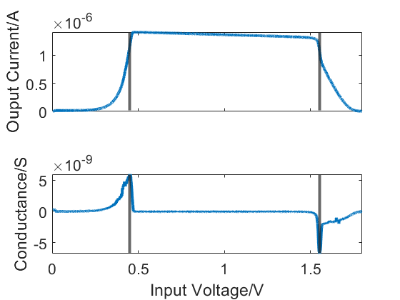
To assess how the window responded to changes in the control devices, the current output is denoised with a 50 sample moving average filter and the differential calculated. The window width is calculated as the difference in input voltage between the minimum and maximum of the derivative (Fig. 3). This method was chosen as it provides a meaningful result in circumstances where the window peak is not constant, where a more common method such as full width at half maximum (FWHM) might not. The differential method typically gives a slightly more pessimistic valuation of the circuit performance than FWHM.
III-A Resistor Array Model

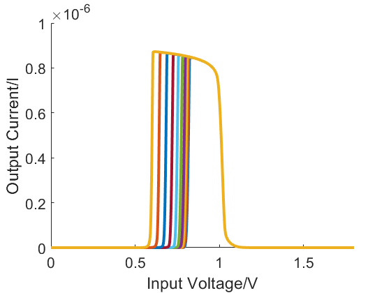
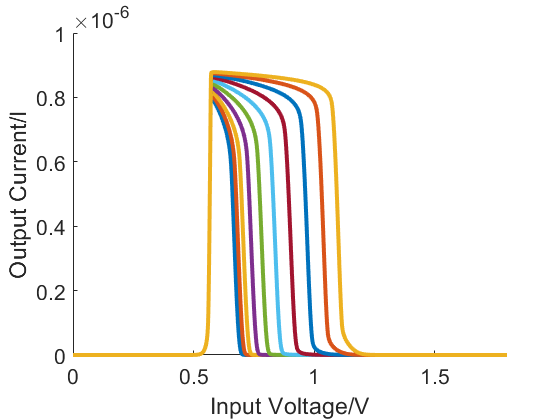
The behaviour of the resistor model was measured by setting one of the dynamic elements to its maximum value and conducting an input sweep at each step of the other dynamic element. In this model, the CAM circuit was supplied at and the input swept from to the supply voltage. The current was measured at every DAC increment, for a total of 5898 samples.
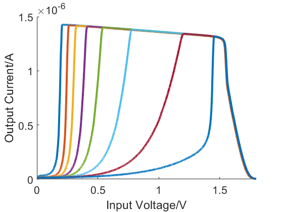
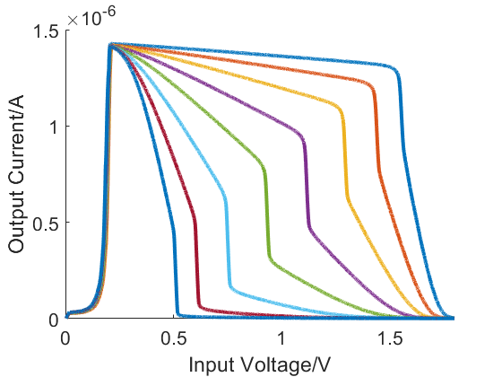
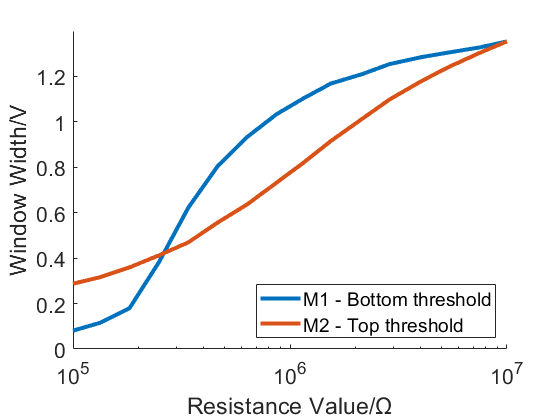
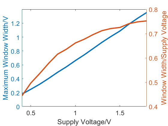
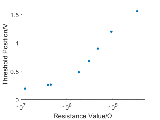
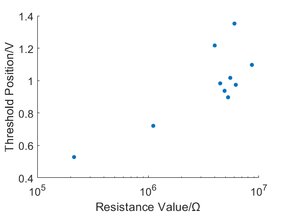
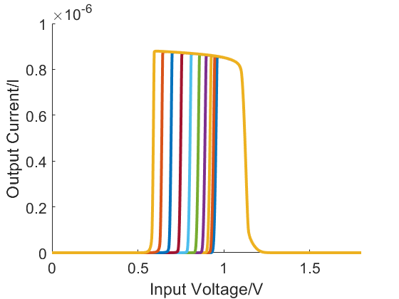
As can be seen in 5, the circuit operates in the intended manner, producing a significant output current at input values between the two thresholds. The upper threshold was measured to be almost linear with the logarithm of the control resistor. The upper threshold displayed the ramp-step-ramp of a current starved inverter. This is because the NMOS in the output branch acts as a voltage follower. This somewhat compromises the specificity of the circuit. The lower threshold displayed significant nonlinearity of control, with a pronounced s-curve. Additionally, the maximum window width was calculated for a range of supply voltages. This was found to be linear, implying that the headroom required is a function of the threshold value of the MOSFETs used, regardless of the operating current.
III-B Memristor Model

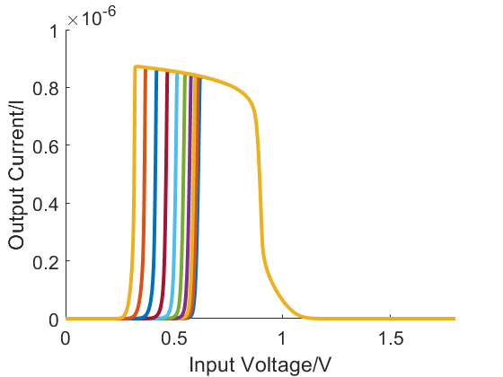
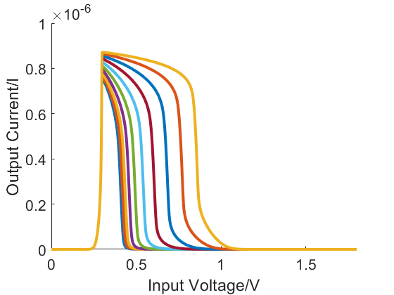
For the memristor tests, the devices were set to a new state with pulses and then read at , before performing a sweep of the input voltage in steps, reading the current at each step for a total of 1801 samples per trace. For the purposes of calculating the threshold position, the current output curve was denoised with the same 50 sample moving average filter. In this case, the same 50 samples represents a larger portion of the trace, but this was required as some of the tests produced exceptionally noisy results. The memristor version of this experiment proved much more challenging to run. The monolayer titanium oxide memristors used in this test are an early memristor technology and come with many of the expected teething issues, presenting difficulty setting new resistive states and holding existing ones. During writing, the state of the devices would relax back towards the previous state and in some tests, the state of the control device would fluctuate. In the sweep of M1, some tests saw the memristor taking random values within a small range, as can be seen in the top right of figure 7. In the sweep of M2, a test at high resistive state saw the control device switching between two distinct values, as can be seen in the outermost trace of the top left of figure 7. This may be indicative of the formation (and disruption) of conductive filaments within the titanium oxide layer, as this is one of the hypothesised mechanisms of the memristive behaviour of these devices[19]. Attempts were made to run tests using bilayer titanium oxide memristors, but the devices used could not be reliably set to resistive states above , which rendered them useless for the bias conditions of this model.
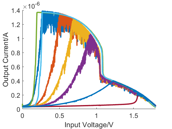
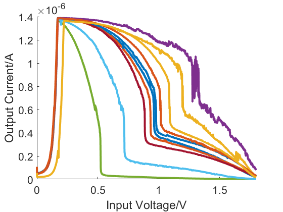
Due to the difficulties holding a device at a specific state, instead of assessing the window width, the position of each threshold was calculated. While this is less useful in characterising the circuit, it prevents issues with setting one threshold from affecting the assessment of the other. Despite this, the tests on the bottom threshold showed a similar s-curve shape to the resistor model. The shape of the window produced is also very similar to the shape obtained in the resistor model. The upper threshold was not so well behaved, showing significant loss in the sharpness of the transition. Further, there was a loss of monotonicity at high resistive states, although this may be due to changes in the state of the M2 device between the measurement taken at the start of each test and the state it held during the test. Despite the irregularities, the traces produce in the tests of the memristor model are clearly of comparable shape and range of position to the results of the resistor model. From this, it can be concluded that resistor models of the circuit can be assumed a reasonable model of the circuit for the assessment of characteristics not explicitly related to the threshold shape, such as power consumption and footprint area.
IV Integrated Simulation
IV-A Design
To estimate the power consumed by the circuit, an integrated circuit model of the design was produced in Cadence Virtuoso using the TSMC180BCD product development kit. This technology node uses planar MOSFETs, for either or . As integrated design provides much greater control of the specifics of the transistors used, three versions of the circuit were designed, with different sizes for the transistor used in the two inverters (Fig. I): one with minimum size input transistors, one with wide input transistors, and one with minimum size native NMOS and conventional PMOS input transistors. In all cases the two transistors on the output branch were minimum size. All transistors are devices. While it may be possible to replace the balancing resistors with static memristors, the assumption is that polysilicon resistors will be used. This constraint makes the balancing resistors of the PCB model wildly impractical, due to the area required. The simulations shown here were conducted with balancing resistors and dynamic resistors of to . While this strips the circuit of a significant portion of its range, it allows for the recovery of much of the sharpness that is now expected to be lost when implemented with memristors. It should be noted that a reduced range is not necessarily a problem, as the circuits before the CAM cell in the signal chain can be designed to output in the operating range of the CAM cell, and may even have their own headroom requirements that make a wider window unnecessary.
| Minimum | Wide | Native | |
|---|---|---|---|
| NMOS Width | |||
| NMOS Length | |||
| PMOS Width | |||
| PMOS Length |
IV-B Assessment
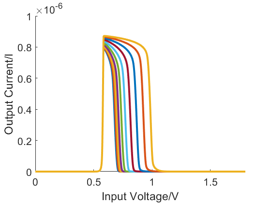
To assess the window width, static DC simulations of the circuits were run. The circuits were supplied at and the inputs swept from to the supply voltage, measuring the current measured at the output. This was repeated for geometrically spaced values of to for the dynamic element. In all cases the output was connected to a dummy load. The window widths were calculated using the same differential method mentioned earlier.
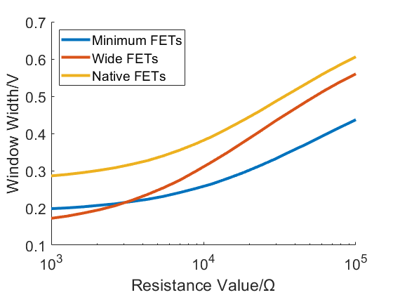
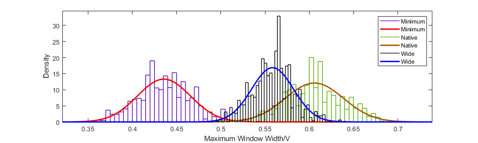
In the circuit with minimum size input transistors, the window width was drastically reduced. Further to this, the range of values for the lower thresholds was roughly half the maximum window width. While the transitions were sharper, this reduced range represents a catastrophic loss of functionality, as a narrow window can only be set in a range. The wide input stage circuit performed much better, losing less maximum window width and retaining most of the threshold sweep of the PCB model. The sharpness of the transitions was also superior to the minimum width circuit, due to the higher gain of the input FETs. The native input stage circuit displayed a wider maximum window width than even the wide circuit, although the minimum size PMOS left it with a lower threshold range comparable to the minimum circuit. The sharpness of transitions in the native circuit were noticeably worse. As one might expect from the lower threshold voltages of native devices, the window of the native circuit was much loser to than the others, which were almost centred in the supply range. In all circuits, plotting the window width as a function of the logarithm of M1 showed less nonlinearity than lower threshold of the PCB model.
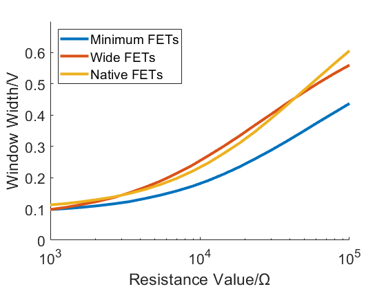
The differences in the behaviour of the top threshold between the three circuits was less pronounced. All three were able to bring the top threshold to within of the bottom threshold. The only significant differences were the inability of the minimum circuit to reach the maximum window widths of the other two, and the less defined transitions of the native circuit.
IV-C Energy
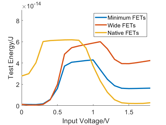
To estimate the energy required to test a single sample, a second gate was added to each of the output transistors as an output enable control, and a transient analysis simulation was run. In this test, the circuit began with the supply energised, the output disabled, and the input parked at either supply or ground. The minimum and wide circuits were parked ant ground and the native circuit parked at supply. The input was brought to the test value and held there for to settle. The enable signal was then pulsed for . after the enable pulse ends, the input is returned to its parked state. The energy was calculated by integrating the sum of the instantaneous power at the input, the enable input, and the supply. As might be expected for an analysis that includes the output current, the test energy of a hit was the peak energy in all cases. Curiously, the miss energy on the opposite side of the window to the parked state was substantially higher than the miss energy on the same side of the window. This is likely because the act of bringing the input signal to the test voltage and back causes the input to pass through both input inverter’s crossover points. This would cause a small surge of current each time, resulting in the observed plateau.
| Minimum | Wide | Native | |
|---|---|---|---|
| Hit Voltage | |||
| Fast/Fast Corner | |||
| Slow/Slow Corner | |||
| Miss Voltage | |||
| Fast/Fast Corner | |||
| Slow/Slow Corner |
| Maximum Window Width at | Minimum | Wide | Native |
|---|---|---|---|
| Fast/Fast Corner | |||
| Slow/Slow Corner |
Further simulations were run at relevant process corners. A corner is a set of environmental or process conditions that might affect circuit performance. Each of the circuits was simulated at four corner conditions: room temperature, body temperature, P/NMOS above specified gain (Fast/Fast), and P/NMOS below specified gain (Slow/Slow). A hit and a miss voltage were chosen for each circuit, to give estimates for a typical use case. The variation with temperature was minimal, but the effect of process variation was substantial, with a Fast/Fast hit dissipating almost twice the energy of a Slow/Slow hit. As the name suggests, a corner is the extreme edge of what one can expect out of the technology, but the variation on display here is sufficient enough to warrant further investigation.
IV-D Process Variation
To obtain a clearer picture of the impact of process variation, a Monte Carlo analysis was conducted. This approach uses a large number of simulations with randomised process variation to provide a statistical model of the expected impact. In this test, the characteristic being monitored is the maximum window width, calculated using the same differential method used earlier. 250 simulations were run for each circuit.
| Minimum | Wide | Native | |
|---|---|---|---|
The resulting histograms of window width show a significant level of variation in the minimum and native circuits. If an error in fabrication causes a gate element to be narrower than intended, the proportional error will be much larger on a minimum size FET than a wider one, so greater variance on the minimum size circuit is to be expected. Why the native circuit has slightly greater variance is not entirely clear, as the larger minimum size of the native FETs should result in marginally less variance, but the low doping level of the native devices likely makes them more vulnerable to fabrication errors there. The wide circuit showed the least variance, both in absolute terms and in proportion of average maximum window width.
With the validity of the model demonstrated, the next was to assess the power dissipation of the circuit. Simulation of the circuit using the TSMC180BCD PDK was conducted for this purpose. Unlike the previous tests, these test used much lower values for the balancing and dynamic resistors, since an integrated resistor with a value of would be prohibitively large. and balancing and dynamic resistors were used. In addition to this, an extra gate was added to both transistors in the output stage, to allow the output to be disabled when the input was being adjusted or the circuit shut down. The energy of a test was obtained by bringing the input from its parked state to the test value and then enabling the circuit briefly after the input stages settled.
V Discussions and Conclusions
As the ratio between dynamic and balancing elements is the only control parameter that has a significant effect, M1 and R1 could swap positions. This would allow for both thresholds to have identical control methods, at the trivial cost of inverting the control of one threshold. With both dynamic elements connected to ground, the devices could be written through the body diodes of the neighbouring NMOS, although this method has yet to be demonstrated. The circuit could be further improved by switching to a smaller technology node, such as . Such a switch would also make the somewhat optimistic control timings described in this work easier to implement.
The circuit considered in this paper demonstrates a highly controllable and flexible analogue content addressable memory cell with acceptable power dissipation. The design has similar area requirements to the work by Can Li et al.[16], with similar functionality. This work has inferior energy dissipation, but the thresholds of the window are sharper and more controllable despite using a smaller range of dynamic element states, with one fifth the ration between minimum and maximum dynamic element values. Further, this work uses a current output rather than a match line. While this is a major factor in the higher energy dissipation, it gives an array of these cells an analogue output. Aside from the obvious use in full analogue neural networks, this also allows for a template matching array based on these cells to tolerate irregularities in the input, such as might be found in neural spike sorting. Compared to the reconfigurable logic gates this work was developed from[15], this work demonstrates a greater degree of controllability for a similar device count and area. While this work does not achieve a comprehensive improvement over existing works, it achieves appreciable improvements in areas relevant to developing fields.
References
- [1] R. Karam, R. Puri, S. Ghosh, and S. Bhunia, “Emerging trends in design and applications of memory-based computing and content-addressable memories,” Proceedings of the IEEE, vol. 103, no. 8, pp. 1311–1330, 2015, DOI: 10.1109/JPROC.2015.2434888.
- [2] G. Pedretti, C. Graves, S. Serebryakov, R. Mao, X. Sheng, M. Foltin, C. Li, and J. W. Strachan, “Tree-based machine learning performed in-memory with memristive analog cam,” Nature Communications, vol. 12, 10 2021, DOI: 10.1038/s41467-021-25873-0.
- [3] C.-S. Lin, J.-C. Chang, and B.-D. Liu, “A low-power precomputation-based fully parallel content-addressable memory,” IEEE Journal of Solid-State Circuits, vol. 38, no. 4, pp. 654–662, 2003, DOI: 10.1109/JSSC.2003.809515.
- [4] H. Liu, “Routing table compaction in ternary cam,” IEEE Micro, vol. 22, no. 1, pp. 58–64, 2002, DOI: 10.1109/40.988690.
- [5] I. Arsovski, T. Chandler, and A. Sheikholeslami, “A ternary content-addressable memory (tcam) based on 4t static storage and including a current-race sensing scheme,” IEEE Journal of Solid-State Circuits, vol. 38, no. 1, pp. 155–158, 2003, DOI: 10.1109/JSSC.2002.806264.
- [6] C. E. Graves, C. Li, X. Sheng, D. Miller, J. Ignowski, L. Kiyama, and J. P. Strachan, “In-memory computing with memristor content addressable memories for pattern matching,” Advanced Materials, vol. 32, no. 37, p. 2003437, 2020, DOI: https://doi.org/10.1002/adma.202003437.
- [7] Y. Pan, P. Foster, J. Huang, A. Serb, and T. Prodromakis, “An rram-based associative memory cell,” 2021.
- [8] M. Hock, A. Hartel, J. Schemmel, and K. Meier, “An analog dynamic memory array for neuromorphic hardware,” in 2013 European Conference on Circuit Theory and Design (ECCTD), 2013, pp. 1–4, DOI: 10.1109/ECCTD.2013.6662229.
- [9] H. Graf and L. Jackel, “Analog electronic neural network circuits,” IEEE Circuits and Devices Magazine, vol. 5, no. 4, pp. 44–49, 1989, DOI: 10.1109/101.29902.
- [10] X. Yin, C. Li, Q. Huang, L. Zhang, M. Niemier, X. Hu, C. Zhuo, and K. Ni, “Fecam: A universal compact digital and analog content addressable memory using ferroelectric,” 04 2020.
- [11] R. Rajaei, M. M. Sharifi, A. Kazemi, M. Niemier, and X. S. Hu, “Compact single-phase-search multistate content-addressable memory design using one fefet/cell,” IEEE Transactions on Electron Devices, vol. 68, no. 1, pp. 109–117, 2021, DOI: 10.1109/TED.2020.3039477.
- [12] ——, “Compact single-phase-search multistate content-addressable memory design using one fefet/cell,” IEEE Transactions on Electron Devices, vol. 68, no. 1, pp. 109–117, 2021, DOI: 10.1109/TED.2020.3039477.
- [13] G. Pedretti, C. E. Graves, T. Van Vaerenbergh, S. Serebryakov, M. Foltin, X. Sheng, R. Mao, C. Li, and J. P. Strachan, “Differentiable content addressable memory with memristors,” Advanced Electronic Materials, vol. 8, no. 8, p. 2101198, 2022, DOI: https://doi.org/10.1002/aelm.202101198.
- [14] R. Rajaei, M. M. Sharifi, A. Kazemi, M. Niemier, and X. S. Hu, “Compact single-phase-search multistate content-addressable memory design using one fefet/cell,” IEEE Transactions on Electron Devices, vol. 68, no. 1, pp. 109–117, 2021, DOI: 10.1109/TED.2020.3039477.
- [15] A. Serb, A. Khiat, and T. Prodromakis, “Seamlessly fused digital-analogue reconfigurable computing using memristors,” Nature Communications, vol. 9, 12 2018, DOI: 10.1038/s41467-018-04624-8.
- [16] C. Li, C. Graves, X. Sheng, D. Miller, M. Foltin, G. Pedretti, and J. W. Strachan, “Analog content-addressable memories with memristors,” Nature Communications, vol. 11, 04 2020, DOI: 10.1038/s41467-020-15254-4.
- [17] P. Foster, J. Huang, A. Serb, S. Stathopoulos, C. Papavassiliou, and T. Prodromakis, “An fpga-based system for generalised electron devices testing,” Scientific Reports, 2022, DOI: 10.1038/s41598-022-18100-3.
- [18] Toshiba, SSM6L36TU LF Datasheet, 2014.
- [19] A. Zaffora, F. Di Franco, R. Macaluso, and M. Santamaria, “17 - tio2 in memristors and resistive random access memory devices,” in Titanium Dioxide (TiO2) and Its Applications, ser. Metal Oxides, F. Parrino and L. Palmisano, Eds. Elsevier, 2021, pp. 507–526, DOI: https://doi.org/10.1016/B978-0-12-819960-2.00020-1.