Resolving the interference of Yu-Shiba-Rusinov states with multi-functionalized STM probe
Abstract
Scattering of superconducting pairs by magnetic impurities on a superconducting surface leads to pairs of sharp in-gap resonances, known as Yu-Shiba-Rusinov bound states. Similarly to the interference of itinerant electrons scattered on defects in normal metals, these resonances reveal a periodic texture around the magnetic impurity. However, the wavelength of these resonances was often too short to be resolved even by methods capable of atomic resolution, like STM. Here, we combine a CO molecule with a superconducting cluster pre-attached to an STM tip to maximize both spatial and energy resolution. The superior properties of such a double-functionalized probe are demonstrated by imaging the interference of YSR states around magnetic Fe dimers on a Nb(110) surface. Our novel approach reveals rich interference patterns of both the even and odd combinations of the hybridized YSR states, which are inaccessible with conventional STM probes.
The invention of the scanning tunneling microscope has revolutionized our understanding of materials and their properties [1]. This progress was made possible by the capability of correlating topographic data of the sample structure obtained by constant-current or constant-height scanning tunneling microscopy (STM) [2] with the data obtained by scanning tunneling spectroscopy (STS) or spin-polarized (SP)-STM. While the former is sensitive to the local density of states [3], the latter grants access to the atomic scale spin structure [4].
However, when performed with normal metal tips, all these methods have their specific limitations, which can be overcome by purposive functionalization. The spatial resolution of topographic STM measurements can be enhanced by attaching a CO molecule to the apex of the STM tip [5, 6], see red circle in Fig. 1. A superconducting probe boosts the energy resolution in STS beyond the thermal broadening limit [7] (green circle) and a magnetic atom at the probe apex acts as a spin sensor in SP-STM measurements [8] (blue). Hereby, the advantages of the probe functionalization not only lie in the improved STM performance, but also in the fact that the probe can sequentially be prepared in a single experimental run by dressing the apex in-situ for specific needs [9].
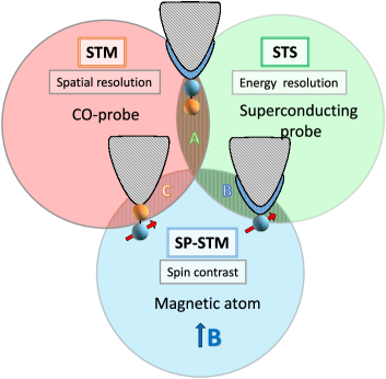
Interestingly, further improvements can be achieved by combining different probe functionalization methods. As sketched in the intersection areas A–C in Fig. 1, this double-functionalization may enable the simultaneous utilization of advantages of several of the above-mentioned methods. For example, as shown in Ref. [10], a combination of a magnetic atom and a superconducting probe can yield a significantly increased spin contrast at the atomic level compared to bulk magnetic tips, which corresponds to the intersection area B in Fig. 1. Similarly, region C covers combinations with magnetic moment-bearing molecules, such as the functionalization with a nickelocene molecule [11, 12], which provides a spin polarization of almost 100% and also leads to an improved spatial resolution. We are not aware, however, of any successful double-functionalization that would cover intersection area A. To address this research gap, we use the combination of a superconducting probe and CO molecule, thus creating double-functionalized CO-SC-probe. The improved spectroscopic and spatial resolution allows us to obtain previously inaccessible details in the local density of states (LDOS) of bound states arising around a pair of magnetic Fe atoms on a superconducting Nb(110) surface.
A single magnetic impurity results in a pair of particle-hole-symmetric sub-gap resonances, known as Yu-Shiba-Rusinov (YSR) bound states. The YSR wave function (i) reflects the shape of atomic orbital responsible for the magnetic scattering channel, (ii) oscillates with the Fermi wave vector , and (iii) decays with increasing distance from the impurity [13, 14, 15]. This decay involves two length scales: an exponential term , determined by the superconducting coherence length , and an algebraic term that depends on the dimension of the system. Since for most elemental superconductors, the algebraic term usually determines the fast attenuation of YSR wave function in three-dimensional materials and precludes the direct detection of its oscillatory behavior.
A successful observation of oscillating YSR states was only possible for systems with a reduced dimensionality of the band structure, such as in quasi-2D superconductors [16, 17], or systems with a strong Fermi surface nesting where parallel flat segments, of the constant-energy contour provide multiple scattering vectors, resulting in the the so-called “focusing effect” with a longer propagation of the YSR along specific directions [18, 19, 20]. Even for a pairs of magnetic impurities, where this effect should be pronounced due to the interference of YSR wave functions from individual atoms [21, 22], the lack of simultaneous high spectroscopic and high spatial resolution limited the experimental access to long-range oscillatory interference patterns. Numerous STS experiments have been performed for various magnetic dimers on different superconducting substrates [23, 24, 25, 26, 27, 28, 29, 30, 31, 9], but usually only show the first maximum of odd and even combinations of the monomer YSR wave function.
By utilizing novel double-functionalized CO-SC-probe tips, we are able to detect these interference patterns in spatially resolved differential conductance maps that correspond to hybridized YSR states of the Fe dimer with even and odd spatial symmetry. We demonstrate the simultaneous enhancement of the spatial and the energy resolution by comparing data obtained on the Fe dimer using the same superconducting probe tip before and after additional functionalization with a CO molecule. Only when the double-functionalized CO-SC probe is used, do the characteristic features in the interference maps appear, which carry information about the Fermi surface of the Nb(110) substrate. A simplified model with an anisotropic Fermi contour allows us to reproduce the focused propagation direction visible in the experimental data. It explains the resulting interference patterns by introducing a Fermi wave vector .
.1 Results
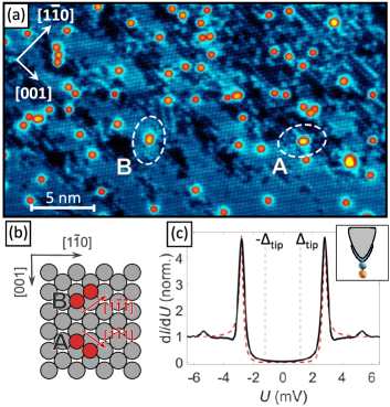
Figure 2(a) shows a constant-current STM image of Fe atoms deposited on a clean Nb(110) surface, taken with the double-functionalized CO-SC probe. The Nb(110) surface with its lattice constant of is atomically resolved. Dark areas in Fig. 2(a) are contaminated with hydrogen and oxygen. The Fe adatoms, visible as bright protrusions, adsorb in four-fold hollow sites of the Nb(110) lattice [32, 33]. Some Fe atoms spontaneously form dimers. In the following, we will focus on those Fe dimers with the shortest interatomic distance, which are roughly oriented along the (dimer A) and the direction (dimer B) [examples marked by ellipses in Fig. 2(a)]. As shown in the schematic drawing of Fig. 2(b), A- and B-dimers are equivalent due to their surface mirror symmetry. It has been shown that these Fe dimers exhibit energy-split YSR states [9].
The tunneling conductance spectrum obtained on the clean Nb surface, see Fig. 2(c), shows well-pronounced coherence peaks shifted by . A pair of weak resonances at can be recognized, which are absent when CO is released from the apex. They correspond to the first vibrational mode of the CO molecule, which—for resonant tunneling in SIS junctions—appears as peaks rather than steps in signal, as is the case for normal-metallic tips [34].
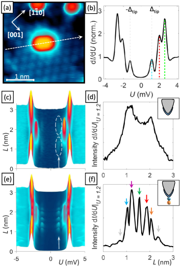
A closer inspection of the zoomed image of the A-type dimer in Fig. 3(a) shows that the dimer axis is slightly rotated clockwise away from the direction (dashed line) [35]. This rotation is most likely caused by the epitaxial strain the Fe dimer experiences if deposited onto a Nb(110) surface. Since the nearest-neighbor distance of bcc-Fe () is smaller than the nearest-neighbor distance along fourfold hollow adsorption sites in the Nb direction (), the Fe atoms will not assume fourfold hollow adsorption sites, but relax inward and shift toward threefold-coordinated sites of the Nb(110) substrate [33]. As a consequence, the dimer axis is slightly tilted clockwise for the A-type and counter-clockwise for the B-type dimer, as confirmed by an inspection of a large number of dimers [9].
In Fig. 3(b), the spectrum measured at the center of the dimer with a CO-SC probe clearly shows two pairs of split YSR resonances, resulting from the hybridization of the YSR bound states of individual Fe atoms. As shown in Ref. [9], the even and odd symmetry of these resonances can already be recognized in maps measured with single-functionalized SC probes. In order to visualize the substantial advantage of double-functionalization, we compare spectra measured along the dimer axis with two types of functionalized probes: a bare SC probe without CO and the same SC probe with a CO molecule attached.
Figure 3(c) shows a waterfall representation of the spectra measured with the bare SC probe along the dashed line in panel (a). In agreement with Ref. [9], the high-energy YSR state at mV exhibits an even symmetry with the strongest signal occurring around the dimer center. In contrast, the low-energy YSR state at shows a much lower intensity and an odd symmetry, with two lobes offset relative to the dimer center, as indicated by two white ellipses. A closer look at the signal profile of the low-energy state at positive range reveals two rather broad maxima that strongly overlap in the center, resulting in a non-zero intensity between the two atoms, see Fig. 3(d).
A completely different picture emerges if a CO molecule is attached to the probe. While the high-energy state preserves its even symmetry with wide maxima in the center, an oscillatory set of peaks becomes visible at the position of the low-energy YSR state, see Fig. 3(e), The clearly improved spatial resolution allows to distinguish up to seven narrow maxima which rapidly decay away from the dimer, as displayed in the line profile in Fig. 3(f). The picture resembles the one taken without CO molecule at large broadening, with the exception of the central peak (marked with a green arrow), where a zero signal is expected for a YSR state with odd-symmetry. The potential origin of this central peak will be discussed below.
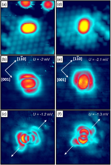
To evaluate the spatial distribution of YSR states, Fig. 4 shows high-resolution maps measured with a double-functionalized CO-SC probe on two different Fe dimers on Nb(110). The data presented in the left and right columns of Fig. 4 correspond to the A-type and B-type dimer shown in the topography maps in Fig. 4(a) and (d), respectively. The energy position of the hybridized YSR states slightly differs for various dimers, which may be caused by the on-site Coulomb potential. At the same time, the relative energy difference remains approximately the same for all measured dimers (). Even a superficial inspection of these experimental maps measured at the high-energy [Figs. 4(b,e)] and low-energy YSR states [Figs. 4(c,f)] reveals interference patterns which carry a much higher degree of details than comparable data obtained with a SC probe without CO [9].
The maps of the high-energy YSR state shown in Figs. 4(b) and (e) exhibit four distinguishable maxima arranged along the nodal plane of the dimer. The maxima have an elongated shape along the dimer axis and the two central ones partially overlap. Such a spatial arrangement is consistent with even-symmetry and explicitly rejects the case with odd-symmetry, since the latter should lead to a vanishing charge density in the entire nodal plane.
A very different interference pattern is observed for the low-energy YSR state, Fig. 4(c) and (f), revealing a sequence of arc-shaped maxima arranged along the dimer axis. Up to three maxima are visible on each side, the intensity of which rapidly decreases with the distance from the dimer. Their arrangement would unambiguously signal an odd symmetry, if it were not for the maximum in the center.
The unexpected position of the maxima on the maps in Figs. 4 is probably caused by the fact that the tunneling conductance depends not only on the convolution of the LDOS of both tip and sample, but also on the tunneling matrix elements between different orbitals. Therefore, the role of the tip tunneling orbital is of fundamental importance. Only if measured with an STM tip governed by an - or -like frontier orbital, the maps reflect the symmetry of the sample wave function.
However, it is known that CO-terminated tips also cause tunneling through the and orbitals [36]. As already discussed in the context of high-resolution imaging of molecular orbitals [37], these frontier orbitals result in maps which represent “the modulus squared of the lateral gradient of the wave functions”, resulting in a contrast inversion at the dimer center. Moreover, it has been pointed out that the “relative contributions from - and -orbitals not only depend on the tip but also on the lateral tip position” [37], thereby potentially giving rise to an unexpected offset and asymmetric distribution of the signal around the Fe dimers in Fig. 4.
Closer inspection of the data presented in Fig. 4(c, f) also indicates that the intensity along the arcs is not uniform, but more concentrated along the direction marked by the arrows, where it experiences a weaker attenuation with distance. Comparison with the crystallographic axes indicated in panels (b,e) reveals that—regardless of dimer orientation—this direction is aligned with the Nb direction. This observation strongly suggests the presence of the aforementioned “focusing effect” in direction.
.2 Theory
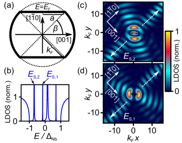
To rationalize our results, we model the experimental data with a simplified 2D continuous model of a bare superconducting surface with an anisotropic stadium-shaped Fermi surface, as shown in Fig. 5(a). A lattice model with a similar Fermi surface was already used in Ref. [38]. We introduce a parameter that defines the length of the flat segments of the Fermi contour, where corresponds to a circular shape with Fermi quasi-momentum . Since the Fermi velocity points always perpendicular to the Fermi surface, a finite generates a focusing of the hybridized YSR-state propagation along the -direction in real space, whose strength increases with increasing .
In the following, we focus our analysis on the LDOS of the impurity-dressed substrate, keeping in mind that the experimental data obtained from STS is actually a convolution of the LDOS of the substrate and the tip. Following the Green’s function approach described in Ref. [20], we model the Fe dimer by adding two magnetic impurities at an inter-impurity distance on the bare superconducting substrate. We fix to the average between the two extremes Fe and Nb with nearest-neighbor distances of and ), as discussed earlier. We also account for the epitaxial strain between the Fe dimer and the Nb(110) substrate, where axis of the Fe dimer is rotated clockwise by an angle with respect to the direction [35]. For simplicity, these impurities are assumed to be identical and described by a semiclassical Shiba model [14] with an onsite energy and an exchange coupling .
In Fig. 5(b), we show the resulting LDOS at one of the impurity sites, which shows two pairs of hybridized YSR states at the energies and . The parameters are are chosen such that the energy difference of the positive and negative pair is .
In Figs. 5(c) and (d), we show the spatially resolved LDOS of the even- and odd-symmetry states at the occupied (hole) part of the high- and low-energy YSR resonances for A-type dimer, respectively. The calculated LDOS maps are in good agreement with the tunneling conductance maps observed experimentally, in particular, they qualitatively reproduce the high (low) LDOS in the nodal plane at for the even- (odd)-symmetric YSR state at [Fig. 4(b)] ( [Fig. 4(c)]). Furthermore, the model reproduces the “focusing effect” in direction, marked with arrows in Fig. 5(d) similar as in Fig. 4(c).
Since the theoretical model is two-dimensional and the attenuation of YSR wave function is significantly reduced, an additional set of maxima in the other direction is also observed. They arise from the remaining circular segment of the Fermi contour and their direction rotates with the orientation of the dimer, whereas the “focusing” direction is independent of the dimer orientation and always directed along . As expected, the calculated data for the odd state in Fig. 5(c) lack the finite signal at the dimer center, which only appears in our experimental data due to the contribution of the CO-related -orbitals.
For the data of Fig. 5, the parameter is chosen to match the oscillation pattern in the experimental data. We find the good match between our theoretical model with a simplified shape of the Fermi contour and the experimental data for , see Fig. S5 in [35]. Surprisingly, this value for estimated for Fe impurity on Nb(110) is almost two times larger than the one obtained for Mn on Nb(110) [39]. It’s important to note, that for Fe atoms the is estimated for YSR states which correspond to scattering channels related to the -orbital, whereas for Mn is obtained for the -orbital [39]. We speculate that the relatively large difference in the effective Fermi wave length for screening magnetic impurities is caused by the fact that the -states of Mn and the -states of Fe hybridize with very different bands of the Nb Fermi surface. Further ab initio calculations would be desirable to clarify this issue.
.3 Discussion
In summary, our results clearly demonstrate the advantages of double-functionalized STM tips which consist of a superconducting cluster and an additional CO molecule attached to it, as they simultaneously enable high energy and extra spatial resolution. The -orbital nature of the CO frontier orbital at the apex of the STM tip results in a higher contrast. Since -like orbital result in a signal which is proportional to the square of the wave function gradient, the image resolution is greatly improved as compared to conventional bulk superconducting or metal probes. Yet, depending on the actual mixture of -, and -like orbitals at the STM tip changes of the symmetry as well as lateral offsets of the features may occur. With an appropriate consideration of these effects, double-functionalized STM tips provide access to the wave functions of YSR bound states on superconductors, as well as, to the character of the Fermi surface of the hosting substrate, which is highly important for studying, for example, unconventional superconductors or systems with topological edge states.
.4 Methods
The experiments are performed in a home-built low-temperature STM at a base temperature of 1.4 K. The Nb(110) surface is cleaned by a series of high-temperature flashes [40]. Fe atoms are deposited in-situ onto the Nb substrate at a temperature of 4.2 K. To get a superconducting probe, an electro-chemically etched W tip was brought in contact with the Nb crystal, thus creating a Nb cluster on the tip apex. CO molecules were picked up from a clean Cu(001) surface using the procedure described in Ref. [9]. The resulting double-functionalized tips exhibit a superconducting gap which corresponds to about 70-90% of the bulk Nb value [41]. The presence of a superconducting gap in the LDOS of the tip causes a corresponding shift of the sample’s LDOS features in the conductance spectra by . The experimental data are measured in the tunneling regime at relatively large tip–sample distances, corresponding to a tunnel resistances , such that the current is dominated by single-electron tunneling rather than Andreev reflections [42, 43, 44, 45]. All spectroscopic measurements are performed with a modulation voltage of 0.1 mV at a frequency of 890 Hz.
References
- Besenbacher [1996] F. Besenbacher, Scanning tunnelling microscopy studies of metal surfaces, Rep. Progr. Phys. 59, 1737 (1996).
- Tersoff and Hamann [1983] J. Tersoff and D. R. Hamann, Theory and application for the scanning tunneling microscope, Phys. Rev. Lett. 50, 1998 (1983).
- Tersoff and Hamann [1985] J. Tersoff and D. R. Hamann, Theory of the scanning tunneling microscope, Phys. Rev. B 31, 805 (1985).
- Bode [2003] M. Bode, Spin-polarized scanning tunnelling microscopy, Rep. Progr. Phys. 66, 523 (2003).
- Gross et al. [2009] L. Gross, F. Mohn, N. Moll, P. Liljeroth, and G. Meyer, The Chemical Structure of a Molecule Resolved by Atomic Force Microscopy, Science 325, 1110 (2009).
- Weiss et al. [2009] C. Weiss, C. Wagner, C. Kleimann, M. Rohlfing, F. S. Tautz, and R. Temirov, Imaging Pauli Repulsion in Scanning Tunneling Microscopy, Phys. Rev. Lett. 105, 086103 (2009).
- Pan et al. [1998] S. H. Pan, E. W. Hudson, and J. C. Davis, Vacuum tunneling of superconducting quasiparticles from atomically sharp scanning tunneling microscope tips, Appl. Phys. Lett. 73, 2992 (1998).
- Loth et al. [2010] S. Loth, C. P. Lutz, and A. J. Heinrich, Spin-polarized spin excitation spectroscopy, New Journal of Physics 12, 125021 (2010).
- Friedrich et al. [2021] F. Friedrich, R. Boshuis, M. Bode, and A. Odobesko, Coupling of Yu-Shiba-Rusinov states in one-dimensional chains of Fe atoms on Nb(110), Phys. Rev. B 103, 235437 (2021).
- Schneider et al. [2021] L. Schneider, P. Beck, J. Wiebe, and R. Wiesendanger, Atomic-scale spin-polarization maps using functionalized superconducting probes, Science Advances 7, eabd7302 (2021).
- Czap et al. [2019] G. Czap, P. J. Wagner, F. Xue, L. Gu, J. Li, J. Yao, R. Wu, and W. Ho, Probing and imaging spin interactions with a magnetic single-molecule sensor, Science 364, 670 (2019).
- Mier et al. [2021] C. Mier, B. Verlhac, L. Garnier, R. Robles, L. Limot, N. Lorente, and D.-J. Choi, Superconducting scanning tunneling microscope tip to reveal sub-millielectronvolt magnetic energy variations on surfaces, Journ. Phys. Chem. Lett. 12, 2983 (2021).
- Yu [1965] L. Yu, Bound state in superconductors with paramagnetic impurities, Acta Physica Sinica 21, 75 (1965).
- Shiba [1968] H. Shiba, Classical spins in superconductors, Progress of Theoretical Physics 40, 435 (1968).
- Rusinov [1968] A. I. Rusinov, Superconcductivity near a paramagnetic impurity, Zh. Eksp. Teor. Fiz. Pisma Red. 9, 146 (1968).
- Ménard et al. [2015] G. C. Ménard, S. Guissart, C. Brun, S. Pons, V. S. Stolyarov, F. Debontridder, M. V. Leclerc, E. Janod, L. Cario, D. Roditchev, P. Simon, and T. Cren, Coherent long-range magnetic bound states in a superconductor, Nature Phys. 11, 1013 (2015).
- Liebhaber et al. [2020] E. Liebhaber, S. A. González, R. Baba, G. Reecht, B. W. Heinrich, S. Rohlf, K. Rossnagel, F. von Oppen, and K. J. Franke, Yu-Shiba-Rusinov States in the Charge-Density Modulated Superconductor NbSe2, Nano Letters 20, 339 (2020).
- Ruby et al. [2016] M. Ruby, Y. Peng, F. von Oppen, B. W. Heinrich, and K. J. Franke, Orbital Picture of Yu-Shiba-Rusinov Multiplets, Phys. Rev. Lett. 117, 186801 (2016).
- Kim et al. [2020] H. Kim, L. Rózsa, D. Schreyer, E. Simon, and R. Wiesendanger, Long-range focusing of magnetic bound states in superconducting lanthanum, Nature Communications 11, 4573 (2020).
- Ortuzar et al. [2022] J. Ortuzar, S. Trivini, M. Alvarado, M. Rouco, J. Zaldivar, A. L. Yeyati, J. I. Pascual, and F. S. Bergeret, Yu-Shiba-Rusinov states in two-dimensional superconductors with arbitrary Fermi contours, Phys. Rev. B 105, 245403 (2022).
- Flatté and Reynolds [2000] M. E. Flatté and D. E. Reynolds, Local spectrum of a superconductor as a probe of interactions between magnetic impurities, Phys. Rev. B 61, 14810 (2000).
- Morr and Stavropoulos [2003] D. K. Morr and N. A. Stavropoulos, Quantum interference between impurities: Creating novel many-body states in s-wave superconductors, Phys. Rev. B 67, 020502 (2003).
- Ji et al. [2008] S.-H. Ji, T. Zhang, Y.-S. Fu, X. Chen, X.-C. Ma, J. Li, W.-H. Duan, J.-F. Jia, and Q.-K. Xue, High-resolution scanning tunneling spectroscopy of magnetic impurity induced bound states in the superconducting gap of Pb thin films, Phys. Rev. Lett. 100, 226801 (2008).
- Ruby et al. [2018] M. Ruby, B. W. Heinrich, Y. Peng, F. von Oppen, and K. J. Franke, Wave-Function Hybridization in Yu-Shiba-Rusinov Dimers, Phys. Rev. Lett. 120, 156803 (2018).
- Meng et al. [2015] T. Meng, J. Klinovaja, S. Hoffman, P. Simon, and D. Loss, Superconducting gap renormalization around two magnetic impurities: From Shiba to Andreev bound states, Phys. Rev. B 92, 064503 (2015).
- Kezilebieke et al. [2018] S. Kezilebieke, M. Dvorak, T. Ojanen, and P. Liljeroth, Coupled Yu-Shiba-Rusinov States in Molecular Dimers on NbSe, Nano Letters 18, 2311 (2018).
- Choi et al. [2018] D.-J. Choi, C. G. Fernández, E. Herrera, C. Rubio-Verdú, M. M. Ugeda, I. Guillamón, H. Suderow, J. I. Pascual, and N. Lorente, Influence of Magnetic Ordering between Cr Adatoms on the Yu-Shiba-Rusinov States of the Superconductor, Phys. Rev. Lett. 120, 167001 (2018).
- Kim et al. [2015] Y. Kim, J. Zhang, E. Rossi, and R. M. Lutchyn, Impurity-induced bound states in superconductors with spin-orbit coupling, Phys. Rev. Lett. 114, 236804 (2015).
- Ding et al. [2021] H. Ding, Y. Hu, M. T. Randeria, S. Hoffman, O. Deb, J. Klinovaja, D. Loss, and A. Yazdani, Tuning interactions between spins in a superconductor, Proc. Natl. Acad. Sci. 118, e2024837118 (2021).
- Küster et al. [2021a] F. Küster, S. Brinker, S. Lounis, S. S. P. Parkin, and P. Sessi, Long range and highly tunable interaction between local spins coupled to a superconducting condensate, Nature Communications 12, 6722 (2021a).
- Beck et al. [2021] P. Beck, L. Schneider, L. Rózsa, K. Palotás, A. Lászóffy, L. Szunyogh, J. Wiebe, and R. Wiesendanger, Spin-orbit coupling induced splitting of Yu-Shiba-Rusinov states in antiferromagnetic dimers, Nature Communications 12, 2040 (2021).
- Küster et al. [2021b] F. Küster, A. M. Montero, F. S. M. Guimarães, S. Brinker, S. Lounis, S. S. P. Parkin, and P. Sessi, Correlating Josephson supercurrents and Shiba states in quantum spins unconventionally coupled to superconductors, Nature Communications 12, 1108 (2021b).
- Odobesko et al. [2020a] A. Odobesko, D. Di Sante, A. Kowalski, S. Wilfert, F. Friedrich, R. Thomale, G. Sangiovanni, and M. Bode, Observation of tunable single-atom Yu-Shiba-Rusinov states, Phys. Rev. B 102, 174504 (2020a).
- Homberg et al. [2022] J. Homberg, A. Weismann, T. Markussen, and R. Bernd, Resonance-enhanced vibrational spectroscopy of molecules on a superconductor, Phys. Rev. Lett. 129, 116801 (2022).
- [35] See Supplemental Material for detailed information.
- Paulsson et al. [2008] M. Paulsson, T. Frederiksen, H. Ueba, N. Lorente, and M. Brandbyge, Unified description of inelastic propensity rules for electron transport through nanoscale junctions, Phys. Rev. Lett. 100, 226604 (2008).
- Gross et al. [2011] L. Gross, N. Moll, F. Mohn, A. Curioni, G. Meyer, F. Hanke, and M. Persson, High-Resolution Molecular Orbital Imaging Using a -Wave STM Tip, Phys. Rev. Lett. 107, 086101 (2011).
- Odobesko et al. [2020b] A. Odobesko, F. Friedrich, S.-B. Zhang, S. Haldar, S. Heinze, B. Trauzettel, and M. Bode, Anisotropic vortices on superconducting Nb(110), Phys. Rev. B 102, 174502 (2020b).
- Schneider et al. [2022] L. Schneider, P. Beck, J. Neuhaus-Steinmetz, L. Rózsa, T. Posske, J. Wiebe, and R. Wiesendanger, Precursors of Majorana modes and their length-dependent energy oscillations probed at both ends of atomic Shiba chains, Nature Nanotechnology 17, 384 (2022).
- Odobesko et al. [2019] A. B. Odobesko, S. Haldar, S. Wilfert, J. Hagen, J. Jung, N. Schmidt, P. Sessi, M. Vogt, S. Heinze, and M. Bode, Preparation and electronic properties of clean superconducting Nb(110) surfaces, Phys. Rev. B 99, 115437 (2019).
- Bose et al. [2005] S. Bose, P. Raychaudhuri, R. Banerjee, P. Vasa, and P. Ayyub, Mechanism of the Size Dependence of the Superconducting Transition of Nanostructured Nb, Phys. Rev. Lett. 95, 147003 (2005).
- Ternes et al. [2006] M. Ternes, W.-D. Schneider, J.-C. Cuevas, C. P. Lutz, C. F. Hirjibehedin, and A. J. Heinrich, Subgap structure in asymmetric superconducting tunnel junctions, Phys. Rev. B 74, 132501 (2006).
- Ruby et al. [2015] M. Ruby, F. Pientka, Y. Peng, F. von Oppen, B. W. Heinrich, and K. J. Franke, Tunneling processes into localized subgap states in superconductors, Phys. Rev. Lett. 115, 087001 (2015).
- Villas et al. [2020] A. Villas, R. L. Klees, H. Huang, C. R. Ast, G. Rastelli, W. Belzig, and J. C. Cuevas, Interplay between Yu-Shiba-Rusinov states and multiple Andreev reflections, Phys. Rev. B 101, 235445 (2020).
- Villas et al. [2021] A. Villas, R. L. Klees, G. Morrás, H. Huang, C. R. Ast, G. Rastelli, W. Belzig, and J. C. Cuevas, Tunneling processes between Yu-Shiba-Rusinov bound states, Phys. Rev. B 103, 155407 (2021).