Parametric Amplifier Matching Using Legendre Prototypes
1 Introduction
Matching networks for active, negative-resistance loads can be used to design Josephson parametric amplifiers (JPA) having specified gain and bandwidth characteristics. Chebyshev JPA matching networks were previously described in [1] and [2], as well as networks based on Butterworth prototypes [1, 3, 4]. A method for calculating prototype coefficients was outlined in [1], Appendix E, including coefficient tables for Chebyshev and Butterworth prototypes.
In this note we describe JPA matching networks based on Legendre polynomials [5]. These networks typically exhibit lower ripple and gentler roll-off than Chebyshev networks with similar parameters, and can be viewed as bridging the gap between Butterworth and Chebyshev ones. We tabulate prototype coefficients for parametric amplifiers based on Legendre polynomials with a range of gain and ripple parameters, and for a range of network orders. We also use this opportunity to further illustrate the synthesis of these networks based on Ref. [1].
2 Legendre Filter Characteristics
Figure 1 shows calculated gain vs frequency for JPAs designed with fourth-order Chebyshev, Butterworth, and Legendre polynomials. All networks were designed for a gain of 20 dB and a 3 dB bandwidth of 500 MHz. While the bandwidth of a Butterworth network is always defined at the 3 dB points, in Chebyshev networks this is only the case for 3 dB ripple designs, i.e., the bandwidth in Chebyshev networks is specified in relation to the ripple. The Legendre networks also specify a “ripple” parameter, but in this case it only controls the gain at the cutoff frequency and not the actual gain ripple in the band. The Chebyshev and Legendre designs in Fig. 1 both specify a ripple parameter of 3 dB.
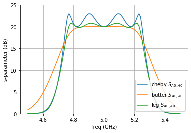
The coupled-modes formalism in [1] describes the strength of the parametric pump via a parameter . This is the parametric coupling rate normalized to , where is the geometric mean of all dissipation rates at the ports of the device. Comparing the designs in Fig. 1, we find that , , and , meaning that, with all other parameters held the same, the Legendre JPA requires higher pump coupling than Butterworth, but lower pump coupling than Chebyshev.
The figure also illustrates the main differences between the various response types. We see that Legendre networks have sharper roll-off than Butterworth ones, but not as sharp as Chebyshev networks. We also see that the ripple in the band is lower in Legendre networks compared with that of Chebyshev network, while for Butterworth networks the pass band is flat.
3 Power Loss Function and 4-Pole Synthesis
We will follow a matching network synthesis flow based on the insertion-loss method. We will go through constructing a power loss function for a Legendre JPA, and then apply the procedure outlined in [1] Appendix E to the specific case of a 4-pole, 20 dB amplifier with 0.5 dB ripple.
3.1 Power Loss Function
The power loss function is defined as
| (1) |
where and are constants and is the Legendre polynomial of order as a function of frequency normalized to the cutoff frequency Hz. The power loss function is related to the reflection coefficient of the network via
| (2) |
For a design with a signal power gain (in linear power units) at the center of the band, we require [1]
| (3) |
Further, for a specified ripple parameter in dB units, we calculate the linear power gain at the cutoff frequency using , where is the signal gain in dB units. We therefore require that at the cutoff frequency
| (4) |
In both Eqs. (3) and (4) we mark the ‘double sideband’ gain quantities with a tilde.
Using the conditions Eqs. (3) and (4) together with Eqs. (2) and (1), we get two equations for and
| (5) | ||||
| (6) |
Note that Eq. (5) explicitly contains . This is because unlike Chebyshev polynomials, is different for different orders. While for odd , it is finite for even , and its value depends on . At the cutoff frequency, we have used for all . Eqs. (5) and (6) can be simplified further for odd- Legendre networks. We now have both and specified in terms of the order of the network, the required gain, and the ripple parameter, and we can write down the power loss function of Eq. (1) as a function of frequency.
3.2 Finding Coefficients for a Fourth-order Network
To illustrate the synthesis flow, we will step through the calculations for extracting the prototype coefficients for a fourth-order Legendre network, matching a JPA for a specified gain of 20 dB with a ripple parameter of 0.5 dB. Note that we do not necessarily recommend the use of 4th order networks, as in most cases 3rd order is sufficient; we do so here just for illustration purposes.
From the gain, ripple, and order, we can write down the power loss function Eq. (1), and from it the reflection coefficient , where we have changed variable to .
| (7) |
Next we need to factor . We first find the complex roots of the -order polynomials in the numerator and denominator, and then reconstruct as a ratio of -order polynomials from a subset of these roots.
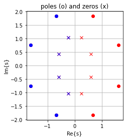
The complex roots of the numerator of , which we will call ‘zeros’, , are:
and the roots of the denominator of , which we call ‘poles’, , are:
Fig. 2 shows the location of the zeros (crosses) and poles (circles) on the complex s-plane. We now choose four out of the eight roots of each of the polynomials, and we pick the ones that are in the left half of the complex s-plane, as shown in blue in Fig. 2. These are from the numerator, and from the denominator.
From the selected roots, we can construct the polynomials and such that ,
| (8) | ||||
| (9) |
and from we can calculate the input impedance of the network, expanding and :
| (10) |
We see that the numerator of the impedance is a fourth order polynomial, and the denominator is a third-order polynomial. We can now perform polynomial long division to express as a continued fraction [1].
| (11) |
The coefficients of the prototype for a fourth-order Legendre matching network with the specified gain and ripple are therefore the coefficients of the continued-fraction expansion
| (12) |
and we have added to the list, representing the conductance of the source.
Following [1], we can now use the coefficients Eq. (12) to find the port coupling , mode couplings , and pump coupling strength for the coupled-mode system representing the amplifier,
| (13) | ||||
| (14) | ||||
| (15) |
where is the full bandwidth of the network.
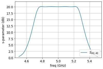
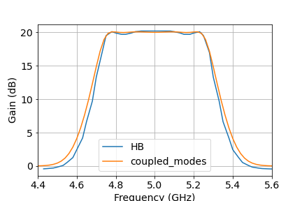
Figure 3 shows the calculated gain profile [1] of an amplifier designed with the coefficients found in Eq. (12), with a center frequency of 5 GHz and a bandwidth of 500 MHz. We find GHz, , , , and . Table 1 lists prototype coefficients for second-, third-, and fourth-order Legendre JPA networks for several gain and ripple parameters.
4 Calculating Circuit Parameters
Following the procedure in [1], we can use the filter prototype coefficients given in Table 1 to calculate device component values based on a coupled-resonator network topology. The procedure requires the following inputs: the order of the filter, , the prototype coefficients , the characteristic impedance of the resonators, the fractional bandwidth of the network , and the center frequency of the network . We will continue with the example in Sec. 3 to design a 4th order Legendre network with GHz, a fractional bandwidth of , gain of 20 dB, ripple of 0.5 dB, and the coefficients in Eq. (12).
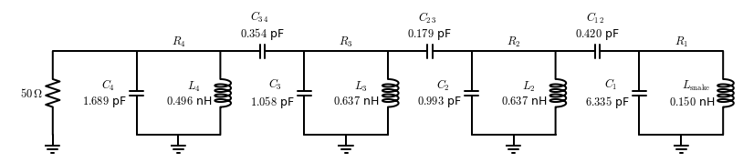
The schematic of the synthesized degenerate amplifier circuit is shown in Fig. 4 as a 1-port network. Resonator on the right contains the nonlinear, parametrically pumped inductance , and the rest of the resonators are passive and constitute the matching network. We label the resonators starting from the parametric element on the right, to align with labeling of the prototype coefficients that regard the parametric element as the source. The nonlinear element we consider here is the ‘snake’, an rf-SQUID array used in Ref. [6], but from a network design point of view, this could equivalently be a standard dc-SQUID [7]. A simulation using Keysight ADS is shown in Fig. 5.
4.1 Resonator Impedances
The first step in calculating circuit component values is to determine the resonator impedances. We first work on resonator in Fig. 4, which contains the capacitively shunted Josephson ‘snake’ element [6]. We target the snake’s operating flux bias point to give pH, so that the impedance of resonator is .
Next, we work on the last resonator, . Normally, the impedance of this resonator can be rather arbitrary, since we could use an admittance inverter , implemented for example as a coupling capacitor, to set the correct coupling strength to the port [1]. However, we would like to avoid an input coupling capacitor because it invariably adds its own, often unacceptable, frequency dependence of the coupling strength. One approach that we will take here, is to constrain the impedance of to give the correct coupling strength to the environment [8], thus obviating the need to use a coupling capacitor (essentially, making trivial). We do so by requiring that , where
| (16) |
This leads to impedance being set to
| (17) |
The rest of the resonator impedances can be now chosen, and we chose .
4.2 Coupling Capacitors
Now that the resonator impedances are set, , , and , we can calculate the rest of the admittance inverter values, and from those, the coupling capacitors.
Inverter will be taken care of by setting the correct pump amplitude, so that the idler presents an admittance of , so that
| (18) |
and there is nothing further we need to do on the circuit design front with respect to this coupling. Inverter is likewise already taken care of by choosing the impedance above.
We are left to determine the values of the rest of the admittance inverters, which we can calculate via
| (19) |
From the admittance inverter values we can calculate the coupling capacitors using
| (20) |
In our design example, we get:
| (21) | ||||
| (22) | ||||
| (23) |
4.3 Resonator Components
Now that the coupling capacitors are calculated, we can continue to construct the resonators in the network, implemented as shunt lumped-element parallel resonators. In each resonator, the capacitor will absorb the negative capacitance associated with its neighboring admittance inverters.
| (24) | ||||
| (25) | ||||
| (26) | ||||
| (27) |
Lastly, we can calculate the inductors easily with , so that nH, and nH. Recall that we already set pH from the outset, by setting the flux bias operating point of the amplifier. This completes the design as shown in Fig. 4.
| Signal gain | ripple | order | ||||||
|---|---|---|---|---|---|---|---|---|
| dB | dB | 2 | 1.0 | 0.2619 | 0.1348 | 1.1528 | ||
| 3 | 1.0 | 0.4924 | 0.4649 | 0.2567 | 0.8674 | |||
| 4 | 1.0 | 0.6884 | 0.7607 | 0.7975 | 0.2304 | 1.1528 | ||
| dB | 2 | 1.0 | 0.3898 | 0.2075 | 1.1528 | |||
| 3 | 1.0 | 0.6304 | 0.6100 | 0.3499 | 0.8674 | |||
| 4 | 1.0 | 0.8099 | 0.9137 | 0.9939 | 0.2996 | 1.1528 | ||
| dB | 2 | 1.0 | 0.4640 | 0.2542 | 1.1528 | |||
| 3 | 1.0 | 0.7020 | 0.6886 | 0.4060 | 0.8674 | |||
| 4 | 1.0 | 0.8661 | 0.9893 | 1.0989 | 0.3413 | 1.1528 | ||
| dB | 2 | 1.0 | 0.6181 | 0.3762 | 1.1528 | |||
| 3 | 1.0 | 0.8459 | 0.8477 | 0.5396 | 0.8674 | |||
| 4 | 1.0 | 0.9598 | 1.1333 | 1.3121 | 0.4440 | 1.1528 | ||
| dB | dB | 2 | 1.0 | 0.2080 | 0.1218 | 1.1055 | ||
| 3 | 1.0 | 0.4084 | 0.4399 | 0.2250 | 0.9045 | |||
| 4 | 1.0 | 0.5833 | 0.7364 | 0.7160 | 0.2244 | 1.1055 | ||
| dB | 2 | 1.0 | 0.3105 | 0.1868 | 1.1055 | |||
| 3 | 1.0 | 0.5244 | 0.5778 | 0.3055 | 0.9045 | |||
| 4 | 1.0 | 0.6886 | 0.8864 | 0.8918 | 0.2903 | 1.1055 | ||
| dB | 2 | 1.0 | 0.3703 | 0.2283 | 1.1055 | |||
| 3 | 1.0 | 0.5849 | 0.6527 | 0.3534 | 0.9045 | |||
| 4 | 1.0 | 0.7379 | 0.9608 | 0.9860 | 0.3295 | 1.1055 | ||
| dB | 2 | 1.0 | 0.4972 | 0.3343 | 1.1055 | |||
| 3 | 1.0 | 0.7066 | 0.8061 | 0.4656 | 0.9045 | |||
| 4 | 1.0 | 0.8219 | 1.1025 | 1.1789 | 0.4239 | 1.1055 | ||
| dB | dB | 2 | 1.0 | 0.1455 | 0.0995 | 1.0579 | ||
| 3 | 1.0 | 0.3074 | 0.3892 | 0.1849 | 0.9453 | |||
| 4 | 1.0 | 0.4552 | 0.6767 | 0.6122 | 0.2094 | 1.0579 | ||
| dB | 2 | 1.0 | 0.2179 | 0.1522 | 1.0579 | |||
| 3 | 1.0 | 0.3964 | 0.5117 | 0.2497 | 0.9453 | |||
| 4 | 1.0 | 0.5401 | 0.8170 | 0.7619 | 0.2688 | 1.0579 | ||
| dB | 2 | 1.0 | 0.2607 | 0.1853 | 1.0579 | |||
| 3 | 1.0 | 0.4432 | 0.5786 | 0.2877 | 0.9453 | |||
| 4 | 1.0 | 0.5806 | 0.8872 | 0.8422 | 0.3035 | 1.0579 | ||
| dB | 2 | 1.0 | 0.3537 | 0.2681 | 1.0579 | |||
| 3 | 1.0 | 0.5380 | 0.7176 | 0.3750 | 0.9453 | |||
| 4 | 1.0 | 0.6516 | 1.0215 | 1.0083 | 0.3849 | 1.0579 | ||
| dB | dB | 2 | 1.0 | 0.1040 | 0.0792 | 1.0321 | ||
| 3 | 1.0 | 0.2369 | 0.3357 | 0.1543 | 0.9689 | |||
| 4 | 1.0 | 0.3639 | 0.6065 | 0.5316 | 0.1912 | 1.0321 | ||
| dB | 2 | 1.0 | 0.1562 | 0.1207 | 1.0321 | |||
| 3 | 1.0 | 0.3066 | 0.4416 | 0.2074 | 0.9689 | |||
| 4 | 1.0 | 0.4338 | 0.7343 | 0.6610 | 0.2439 | 1.0321 | ||
| dB | 2 | 1.0 | 0.1872 | 0.1466 | 1.0321 | |||
| 3 | 1.0 | 0.3435 | 0.4998 | 0.2382 | 0.9689 | |||
| 4 | 1.0 | 0.4675 | 0.7987 | 0.7305 | 0.2743 | 1.0321 | ||
| dB | 2 | 1.0 | 0.2560 | 0.2103 | 1.0321 | |||
| 3 | 1.0 | 0.4189 | 0.6216 | 0.3081 | 0.9689 | |||
| 4 | 1.0 | 0.5282 | 0.9227 | 0.8748 | 0.3441 | 1.0321 |
References
- [1] Ofer Naaman and José Aumentado “Synthesis of Parametrically Coupled Networks” In PRX Quantum 3 American Physical Society, 2022, pp. 020201 DOI: 10.1103/PRXQuantum.3.020201
- [2] W.. Getsinger “Prototypes for Use in Broadbanding Reflection Amplifiers” In IEEE Transactions on Microwave Theory and Techniques 11.6, 1963, pp. 486–497 DOI: 10.1109/TMTT.1963.1125715
- [3] Bengt T Henoch “A new method for designing wide-band parametric amplifiers” In IEEE Transactions on Microwave Theory and Techniques 11.1 IEEE, 1963, pp. 62–72
- [4] Tanay Roy et al. “Broadband parametric amplification with impedance engineering: Beyond the gain-bandwidth product” In Applied Physics Letters 107.26 AIP Publishing LLC, 2015, pp. 262601
- [5] M.. Chryssomallis and J.. Sahalos “Filter synthesis using products of Legendre polynomials” In Electrical Engineering 81.6 Springer, 1999, pp. 419–424 DOI: 10.1007/BF01387163
- [6] Theodore White et al. “Readout of a quantum processor with high dynamic range Josephson parametric amplifiers” In Applied Physics Letters 122.1, 2023, pp. 014001 DOI: 10.1063/5.0127375
- [7] JY Mutus et al. “Design and characterization of a lumped element single-ended superconducting microwave parametric amplifier with on-chip flux bias line” In Applied Physics Letters 103.12 American Institute of Physics, 2013, pp. 122602
- [8] O Naaman et al. “High saturation power Josephson parametric amplifier with GHz bandwidth” In 2019 IEEE MTT-S International Microwave Symposium (IMS), 2019, pp. 259–262 IEEE