SQUID current sensors with an integrated thermally actuated input current limiter
Abstract
The development of SQUID current sensors with a thermally actuated input current limiter (TCL) integrated into the input circuit of the sensor is presented. The TCL is based on an unshunted Josephson Junction (JJ) series array, around which meanders a galvanically isolated, but tightly, thermally coupled, resistive heater element. By applying a current to the heater, the JJ critical currents can be reduced or completely suppressed, while the other on-chip SQUID circuit elements remain unaffected. The functional parameters of the TCL are determined by direct transport measurements and by static and dynamic flux coupling tests via the input circuit. In liquid Helium, a heater power, which reliably suppresses the critical current of the JJ array to zero, of 1.5 mW was needed, with the TCL normal state resistance being at 500 . In this configuration, typical TCL switching times below 10 s were observed in the direct transport measurements.
The TCL can be used to temporarily or even permanently disable malfunctioning channels in multichannel SQUID magnetometer systems, when feedback into their otherwise superconducting input circuits is not possible. In doing so, significant signal distortions in neighbouring channels from screening currents in these input circuits are avoided. Furthermore, by completely suppressing and restoring the TCL critical current, dc offset currents in the superconducting input circuits can be prevented. This is relevant, for instance, in SQUID-based spin precession experiments on hyperpolarized noble gases, in which even dc currents of a few A in the input circuit can lead to significant magnetic field distortions in the adjacent sample region contributing to the transverse spin-spin relaxation rate .
Keywords: SQUID current sensor, current limiter, thermal switch
\ioptwocol
1 Introduction
The superconducting quantum interference device (SQUID) forms the basis of many highly sensitive measurement devices [1] and one of the most common arrangements is the current sensing SQUID. Here, the SQUID is usually inductively coupled to an on-chip input coil which, if used as a magnetometer, can be connected to a superconducting pick-up coil. This broadband detection scheme is deployed in biomagnetism, where multichannel systems map the magnetic fields emanating from the human body. Other applications require the use of pulsed fields prior to a detection period, e.g., ultra-low field magnetic resonance imaging (ULF MRI) [2] or magnetorelaxometry (MRX) [3]. In these cases, the SQUID circuitry must be protected from potentially large currents in the input circuit which tend to trap flux in the form of vortices in the superconducting on-chip structures. Arbitrary motion, such as thermally activated agitation of such vortices, would lead to excess low frequency noise which degrades the performance of the device.
One method to mitigate this problem is to limit the current in the superconducting input circuit, by incorporating either a series Josephson Junction (JJ) array [4] or a series SQUID array [5]. In both cases, the signal current in the superconducting input circuit cannot exceed the critical current of the JJ- or SQUID series array. Even though can also be modulated externally by applying a magnetic field to this type of current limiter, it cannot be set precisely to zero. Another approach is to thermally drive part of the superconducting input circuit leads into its normal state. This scheme is used, for instance, in a so-called cryoswitch [6] (Supracon SW1). The cryoswitch, when not actuated, does not restrict the input current, though it could be combined with a JJ- or SQUID-based input current limiter.
In this work, those approaches are combined in a design that employs a series array of JJs as well as a resistive heater. As a result, a compact, fully integrated, thermally actuated current limiter (TCL) is presented which offers a well-defined low critical current and the ability to set 0.
2 Design of thermally activated switch
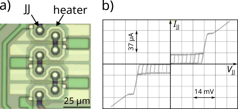
The TCL consists of a series array of 8 unshunted JJs, around which meanders a galvanically isolated heater, formed by a thin-film resistor as shown in figure 1a). The window-type JJs are fabricated using the established Nb-Al(AlOx)-Nb trilayer technology, each having a nominal equivalent square length of 4.5 m and a critical current density, , of approximately 75 A/cm2. The heater resistor is placed on a region of the bottom electrode of the JJ array structure, on which an insulating oxidized niobium Nb2O5 surface layer is formed by anodic oxidation. An additional insulating layer of SiO2 is deposited on top of the Nb2O5 surface by plasma-enhanced physical layer deposition (PECVD). This is done to provide sufficient electrical insulation between the heater and the JJs. The insertion of such an insulating layer does not deteriorate the heater efficiency, which has been validated by measurements on a set of samples with reduced SiO2 thickness and with Nb2O5 insulation only.
From the measured - curve of a TCL without an applied heater current, as shown in figure 1 b), a maximum critical current, , of 15 A and a normal state resistance, , of 500 are determined. Since the TCL is integrated into the superconducting input circuit, its normal state resistance – when the TCL is activated – acts as a thermal current noise source with the power spectrum density 4, where is the Boltzmann constant and is the temperature of the resistance . This noise can couple to neighbouring channels via the mutual inductances of their input circuits. Therefore, should be sufficiently large to minimize this additional noise.
3 Performance
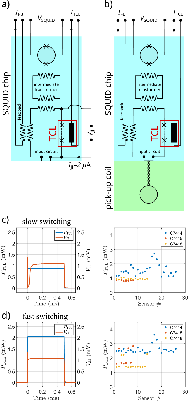
The TCL switching performance was tested at 4.2 K in liquid Helium. Two methods, as shown in figures 2 a) and b), were used. Firstly, the dependence of the voltage across the JJ array, , was measured with respect to applied dc heater power . Here, a small current of 2 A was applied to the JJs in order to generate an easily measurable voltage drop across the array. In the second method, we measured the flux coupling between the input circuit and the SQUID by applying a current into the feedback coil and then observing the SQUID voltage-flux characteristics (in open loop) for different values of . This TCL test has the advantage of being able to be performed in the final, assembled sensor arrangement.
The results using the first approach are shown in figures 2 c) and d). As expected, the switching time, as defined as the time, after which all JJs are in the voltage state, depends on . There is some variation in the performance for different fabrication runs. In particular, the early devices (C7414) show significant spread which can be attributed to inhomogeneous fabrication parameters. For later devices (C7415 and C7418), we observed switching times of approximately 200 s for 1 mW (slow switching). For 1.5 mW, the switching time was below 10 s (fast switching). Note, for the coupling measurements, the switching times were shorter for the same because not every JJ has to be in the normal state to prevent coupling (data not shown).
4 Multichannel SQUID system
4.1 Noise performance
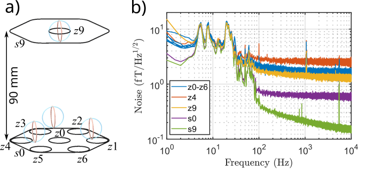
The current sensing SQUIDs with integrated TCL were mounted onto our 18-channel prototype, multichannel SQUID system [7] and its noise performance was investigated inside the heavily shielded room BMSR2.1 in the Physikalisch-Technische Bundesansalt (PTB) in Berlin. The system was situated centrally inside the room and operated with commercial, multichannel read-out electronics (Magnicon, MCFLL) [8]. The electronics were operated outside of the shielded room to avoid detrimental magnetic fields, caused by electronic components which could have worsened the field homogeneity of the heavily shielded environment.
The noise performance of the channels is shown in figure 3. As observed previously [7], the bottom channels, 0-6 and 0, are dominated by dewar noise and show a white field noise density of approximately 1.5 and 0.6 fT/Hz1/2, respectively. The 4 channel has an intrinsically higher SQUID noise. The 9 channel noise level of 1.25 fT/Hz1/2 stems from SQUID and electronics contributions, whereas the upturn in the 9 noise from 0.15 fT/Hz1/2 at 10 kHz towards lower frequencies is generated by the -metal walls of the BMSR2.1 [9].
4.2 Avoiding signal distortions
In addition to protecting the input circuit from too large currents, an important feature of our TCL is the ability to deactivate a given sensor channel by permanently ’opening’ its input circuit. This would for example be necessary, if a faulty SQUID or feedback coil were to prevent feedback into the input circuit. When the feedback works properly, any input circuit current is effectively nulled and signal cross-talk between channels from mutual input circuit couplings is minimized. If feedback into the input circuit of a given channel were not possible, while its input circuit remains fully superconducting, any field change would give rise to shielding currents which, in turn, would couple into neighbouring channels via mutual inductance (mainly due to the mutual inductance of the pick-up coils). Permanently activating the TCL of the faulty channel prevents this parasitic coupling between sensor channels.
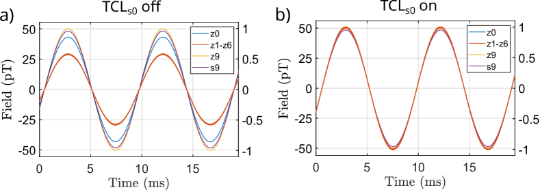
To demonstrate this effect, a homogeneous field of 50 pT was applied in the -direction, while the large bottom 0 pick-up coil was not operated, i.e., feedback circuit open. In figure 4 a), the TCL was not operated, leading to screening currents in 0 and causing large signal size distortions in the flux locked loop signals of the other functioning channels. A reduction of more than 40% was observed for the strongly coupled 1-6 coils adjacent to 0. For the central 0 coil, a smaller reduction of 14% was observed, whereas 9 was hardly affected. The distortions are removed by operating the 0’s TCL leading to the same signal amplitude being recovered for all -channels as expected for a homogeneous driving field, as shown in figure 4 b).
With knowledge of the pick-up coil geometry, this effect can be quantified. The flux, , in a pick-up coil with area , due to a homogeneous field , is . When sensor is not operated, a shielding current is induced, where is the total input circuit inductance of sensor . This leads to a screening flux in the pick-up coil, , of , where is the mutual inductance between pick-up coils and . The ratio of the screening and signal flux in is then . Finally, we obtain for the measured field in including screening effects due to :
| (1) |
In table 1, the calculated values are shown for -sensors taking screening due to 0 into account. The predicted values, using the computed , , and the independently measured , are in very good agreement with observation shown in figure 4 a).
-
coil (nH) 0 3.86 0.86 1-6 11.7 0.575 9 3.40 0.993
4.3 Avoiding additional magnetic field gradients
In order to demonstrate the detrimental effects of an additional magnetic field gradient, caused by a trapped dc current in a superconducting pick-up coil, high-precision spin precession experiments of hyperpolarized 3He were carried out as shown in figure 5. Noble gases, such as 3He, have intrinsic hours-long spin-lattice and spin-spin relaxation times and , respectively [10]. However, this gaseous spin system is particularly sensitive to even minute field gradients leading to -shortening. The sample contained 777 mbar of 3He at room temperature and was polarized offline by spin-exchange optical pumping [11]. For our experimental conditions the so-called high pressure regime applies, where the spin-spin relaxation rate can be approximated to [12]:
| (2) |
where, 1.55 cm is the radius of a spherical sample cell, 32.43 Hz/T is the gyromagnetic ratio of 3He, is the spatial gradient of the static holding field, which in this case is in the -direction, and 1.54 cm2/s is the diffusion constant of the 3He atoms.
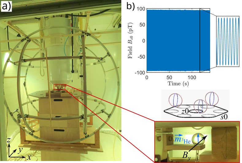
Figure 6 a) shows the measured for the different conditions. For , exhibits an intrinsic time dependence (blue data points), which we attribute to a time-varying gradient . This could be modelled phenomenologically by a second-order polynomial and likely originated from drifting background gradients or dynamic self-interactions due to the non-spherical sample. When currents of 10, 20 and 40 A were trapped solely in the 0 pick-up coil, was markedly reduced, with the effect becoming more pronounced with increasing . The application of currents larger than the nominal critical current of 15 A was possible due to degraded JJ characteristics. To obtain the additional -shortening contribution due to trapped current , we introduce and express the resulting effective spin-spin relaxation rate by:
| (3) |
where the observed time dependence for 0 is absorbed into an intrinsic given by (2).
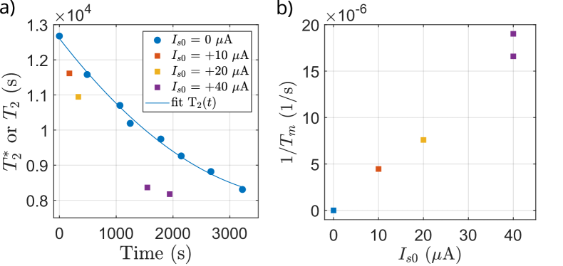
Figure 6 b) shows a roughly linear relationship between and . One would expect , since the additional is linear with and its functional dependency should follow (2). The likely cause for this discrepancy is the assumption that the time varying intrinsic gradient and the additional gradient, due to , are strictly linear in all directions and therefore, purely additive over the entire sample volume. In particular, the strict linearity of the additional gradient due to in the close-by pick-up coil is an oversimplification. Nevertheless, significant -time shortening is observed, when a dc current is trapped in which can be prevented by actuating the TCL thereby setting 0.
In the following, a rough estimation of the gradient due to the current is presented, where we neglect the off-diagonal elements, such that . Assuming a circular pick-up coil of diameter 37 mm (equivalent radius of sensor 0), the main gradient at the sample position underneath the coil would be along the coil’s normal vector, i.e., the -axis. It can be shown, , which occurs when . From Gauss’s law, div B0, , implying an expected value of 2.0 pT/(cmA).
The resultant can then be calculated using (2). For 10, 20 and 40 A, the computed values for are 310-6, 1210-6 and 4810-6 1/s, respectively. At higher , the difference between the observed approximately linear behaviour and the predicted quadratic dependency again becomes apparent, whereas at low , there is good agreement with the measured results shown in figure 6 b).
5 Conclusion
In conclusion, we have presented a compact, fully integrated, thermally activated current limiter, which in addition to limiting the input circuit current to about 15A, can be used to set the input coil critical current to zero. The TCL can be activated within 10 s with a power of approximately 1.5 mW. In addition to pulsed fields applications, it is particularly useful for the deactivation of non-functioning channels, avoiding parasitic signal distortions due to shielding currents in their fully superconducting input circuits. In the field of high-precision spin precession experiments, detrimental gradients due to trapped dc currents can also be avoided, ensuring the best possible experimental conditions.
References
References
- [1] Clarke J and Braginski A I (eds) 2006 The SQUID Handbook vol 2 (Wiley)
- [2] Kraus Jr R, Espy M, Magnelind P and Volegov P 2014 Ultra-Low Field Nuclear Magnetic Resonance: A New MRI Regime (Oxford University Press) ISBN 978-0-19-979643-4
- [3] Arsalani S, Radon P, Schier P P, Jaufenthaler A, Liebl M, Baumgarten D and Wiekhorst F 2022 Physics in Medicine & Biology
- [4] Hilbert C, Clarke J, Sleator T and Hahn E L 1985 Applied Physics Letters 47 637–639
- [5] Drung D, Assmann C, Beyer J, Kirste A, Peters M, Ruede F and Schurig T 2007 Applied Superconductivity, IEEE Transactions on 17 699–704 ISSN 1051-8223
- [6] Zotev V S, Matlashov A N, Volegov P L, Urbaitis A V, Espy M A and Jr R H K 2007 Supercond. Sci. Technol. 20 S367
- [7] Storm J H, Drung D, Burghoff M and Körber R 2016 Superconductor Science and Technology 29 094001
- [8] Bechstein S, Drung D, Scheiner M, Petsche F, Valiollahi S A, Körber R and Barthelmess H J 2020 Journal of Physics: Conference Series 1559 012001
- [9] Storm J H, Hömmen P, Drung D and Körber R 2017 Appl. Phys. Lett. 110 072603
- [10] Gemmel C, Heil W, Karpuk S, Lenz K, Ludwig C, Sobolev Y, Tullney K, Burghoff M, Kilian W, Knappe-Grüneberg S, Müller W, Schnabel A, Seifert F, Trahms L and Baeßler S 2010 The European Physical Journal D 57 303–320
- [11] Korchak S E, Kilian W and Mitschang L 2012 Applied Magnetic Resonance 44 65–80
- [12] Cates G D, Schaefer S R and Happer W 1988 Physical Review A 37 2877–2885