Anomalous Electronic Transport in High Mobility Corbino Rings
Abstract
We report low-temperature electronic transport measurements performed in two multi-terminal Corbino samples formed in GaAs/Al-GaAs two-dimensional electron gases (2DEG) with both ultra-high electron mobility ( and with distinct electron density of and . In both Corbino samples, a non-monotonic behavior is observed in the temperature dependence of the resistance below 1 . Surprisingly, a sharp decrease in resistance is observed with increasing temperature in the sample with lower electron density, whereas an opposite behavior is observed in the sample with higher density. To investigate further, transport measurements were performed in large van der Pauw samples having identical heterostructures, and as expected they exhibit resistivity that is monotonic with temperature. Finally, we discuss the results in terms of various lengthscales leading to ballistic and hydrodynamic electronic transport, as well as a possible Gurzhi effect.
I Introduction
Over the last two decades, great progress has been achieved in increasing the electron mobility in two-dimensional electron gases formed in MBE-grown materials such as GaA/AlGaAs and alternatively in exfoliated graphene. Spectacularly, the electron mobility in GaAs/AlGaAs 2DEGs has recently been reported to reach Chung2022 and, in the absence of phonons at low temperatures, this results in large impurity-dominated mean free path that can exceed . These high-mobility 2DEGs are notoriously well described by Fermi liquid theory at low temperatures, but what is perhaps less obvious is that counter-intuitive phenomena can arise as a result of an interplay between hydrodynamic transport and confinement. As an example, Gurzhi noted in 1963 Gurzhi1963 ; Gurzhi1968 that if a Fermi liquid is confined in a narrow constriction of characteristic size , within some restrictive conditions the resistance of the metal could decrease with increasing temperature. More recently, studying the scattering lengths in 2D semiconductors with moderately high electron mobility, Ahn and Das Sarma Sarma2022 proposed that Gurzhi’s prediction could occur even in bulk GaAs 2DEGs with sufficiently short electron-electron scattering lengths and low disorder.
Motivated by these works, we have fabricated two identical multi-terminal Corbino rings in GaAs/AlGaAs 2DEGs with electron mobility exceeding , and with two different electron density leading to distinctive electron-electron and electron-impurity scattering lengths. Four-point conductance (resistance) measurements were performed in these Corbino with a transport channel defined by a annular ring probing only the bulk of the sample, i.e. with no edge. These measurements are compared with similar measurements performed in millimetre scale van der Pauw (VdP) samples that have the same heterostructure. We note the intrinsic resistivity (conductivity) in the VdP and Corbino samples differs from the measured resistance (conductance) solely by a geometric factor and therefore both will be used interchangeably in the text below. Astonishingly, the temperature dependence of both multi-terminal Corbino shows an anomalous temperature dependence whereby in one case a sharp decrease in resistance is observed at temperatures below 1 with increasing temperature, and an opposite behavior is observed in the other Corbino sample. In the van der Pauw (VdP) samples with identical heterostructure to the multi-terminal Corbino, as expected a monotonic behavior of resistivity with temperature was observed.
II Results
Corbino and van der Pauw geometry. Typical measurements performed in large 2DEG samples usually utilizes either samples prepared in van der Pauw or Hall bar geometry. In the VdP geometry, the electrical contacts are located in each corner and midpoint along the perimeter of a square wafer of size mm in our case. Four-point measurements are then performed by applying a fixed current (voltage) and measuring voltage (current) using a combination of four contacts. Even though non-patterning helps to preserve the pristine state of the ultra-high quality 2DEG, transport measurements performed in either VdP or Hall bar unavoidably contain both the bulk and surface (or more precisely the edge) effects. In the case where only the bulk contribution to the resistivity (or conductivity) is wanted, one can have recourse to the Corbino geometry where the sample contacts are prepared in a circular/ring geometry, with the active region of the 2DEG sample defined by an annulus. In this case, the current is applied concentrically from the outer to inner radii and the electronic transport measurements solely probe the bulk of the sample. Most studies performed so far in the Corbino geometry have focused on samples with an inner contact and a single outer ring and these are inherently two-point contact measurements where unfortunately the contact resistance with the 2DEG is not eliminated. However, multi-terminal Corbino samples possessing one inner contact and three outer rings can be fabricated for four-point measurements, see FIG.1(a). While the Corbino geometry does not have any edge nor radial dimension, however it does have a channel length which is defined as the distance between the inner diameter of the third ring ( probe) and the outer diameter of the second ring ( probe). In our case, this channel length is for both Corbino samples.
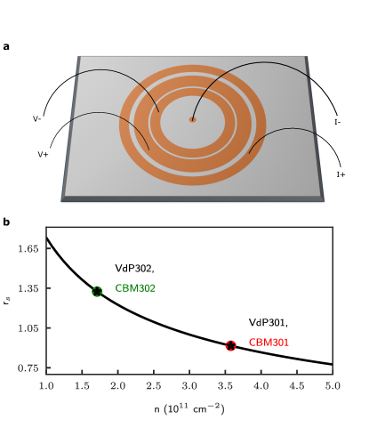
Electron density and parameter. The dimensionless electron-electron interaction parameter , where is the electron density of either set of samples, and is the effective Bohr magneton radius, are 0.92 and 1.32 for the 301 and 302 wafers, respectively, and they are shown in FIG.1(b). Given its significantly higher value and ultra-high electron mobility, the 2DEG formed in 302 samples (when compared to 301) are expected to inherently have enhanced electron-electron interaction, and conversely significantly distinct electron-electron scattering lengths versus temperature.
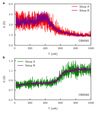
Four-point Corbino conductance measurements. Electronic transport measurements were carried on with the multi-terminal Corbino samples. In this geometry, it is usual to measure the conductance and for this reason we first show the measured conductance versus temperatures in both samples. We performed these measurements with two distinct measurement circuits, labeled setup A (20 excitation current) and setup B (83 excitation current), see supplementary material (SM). These results are shown in FIG.2(a) for CBM301 and FIG.2(b) for CBM302, and the data obtained with each circuit are in excellent agreement with one another. The temperature dependence of conductance measured in CBM301 shows a decrease in conductance at temperatures above 400 , which at first sight may not be surprising given there has been reports of increasing electron mobility well below 1 in 2DEGs of moderately high mobilityUmansky1997 . Surprisingly, a completely opposite trend is observed for CBM302 where an anomalous increase in conductance (decrease in resistance) with increasing temperature is observed at temperatures above 500 . The resulting fractional change in conductance () is between 500 and 700 , and this is different from the anomalous transport behavior observed in CBM301 in spite of both samples having an identical geometry and similar high electron mobility.
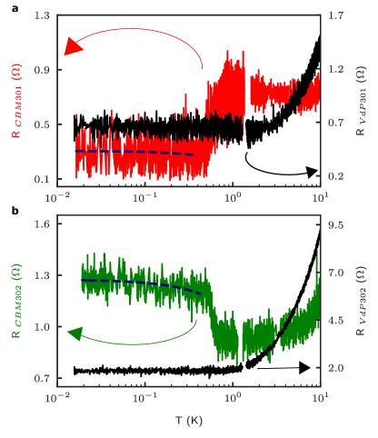
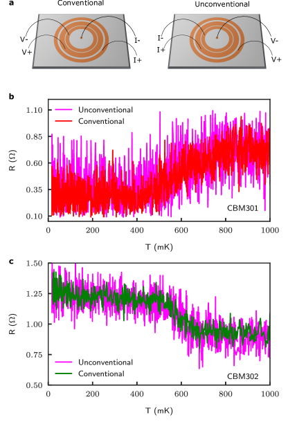
Probe symmetry and reciprocity theorem. To further validate our observation, we have performed conventional and unconventional transport measurements in both Corbino samples, see FIG.3. Note that in this figure, and in the remainder of the text we opted to report and discuss the resistance versus temperature rather than the conductance. In the unconventional configuration, the current () and voltage () probes are interchanged and this results in the Corbino geometry for the current probes, somewhat counterintuitively, to be connected to intermediate rings, and the voltage probes to the most outer and inner contacts, see FIG.3(a). The reciprocity theorem of electromagnetism which traces its roots to Maxwell’s equations (and has been connected to Onsager’s relations by Casimir Casimir1963 ) states that both configurations should yield the same measurement. This holds true for passive circuits that are composed of linear media and for which time-reversal symmetry is not broken. Our reciprocity measurements are shown in FIG.3(b) and (c), with the data shown in magenta taken in the unconventional configuration. Except for the higher noise floor, the measurements clearly satisfy the reciprocity theorem, adding strength to the observation of anomalous transport in the multi-terminal Corbino samples.
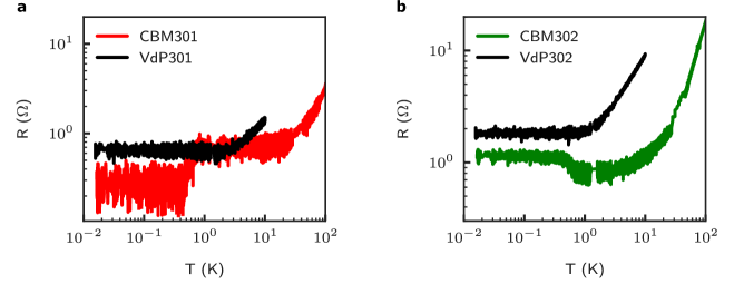
Comparison of Corbino and van der Pauw measurements. van der Pauw measurements were performed to determine the bulk resistivity of each parent heterostructure. Fig.4(a) and (b) shows the resistance measured in both Corbino and VdP samples up to 10 temperature on a semi-log scale. The resistance of VdP301 shows a very slight decrease up to 2 which is then followed by the expected monotonic increase due to scattering with phonons. This behavior is drastically distinct from CBM301 which exhibits a sudden increase in resistance at 400 , followed by a saturation over a wide range of temperatures, up to 10 . In the case of VdP302, the increase in resistance due to phonons onsets near 1 , and as expected is followed by a monotonic increase with temperature, see Fig.4(b). This greatly contrasts with the sudden decrease in resistance observed in CBM302 near 500 , followed by a saturation up to a temperature of 3 where a monotonic increase with temperature is observed. We also note that in all cases the resistance is nearly constant at temperatures below 0.5 , as expected in very high-mobility GaAs/AlGaAs 2DEGs, hence ruling out the anomalous behaviour in electronic transport observed being caused by a percolation process (metal-insulator transition). Recent work also found that under some conditions NiGeAu used to create the electrical contacts could be superconducting with a transition temperature around 700 and with a critical field of 0.15 Ritchie2020 ; Saunders2022 . In order to investigate if a supercurrent and/or a proximity effect could have played a role in our transport measurements, two-terminal and four-terminal differential resistance measurements under a DC current bias were performed at base temperature of the dilution refrigerator () and the obtained were found to be linear (Ohmic). In addition, we have performed magneto-transport measurements in a perpendicular field near the expected critical field (also at base temperature) and found no evidence of superconductivity in either samples, see SM. Finally, additional electronic transport data up to 100 in the Corbino and up to 10 in the VdP samples are provided in the SM that illustrates the distinctive behaviour between the VdP and CBM samples at temperatures below a few Kelvins.
III Discussion
Transport lengthscales. As discussed in Ref. Sarma2022 , the relevant lengthscales that are impacting the bulk resistivity of a high-mobility 2DEG are: (A) The momentum-conserving mean free path due to electron-electron interaction, ; (B) the momentum-relaxing mean free path due to electron scattering with both impurities and phonons, ; and (C) the width of the annular region forming the transport channel which is in our case. When phonons contribute negligibly to electron scattering, which has been shown to be the case below temperature Sarma2008 , the momentum-relaxing mean free path can be calculated from the mobility and electron density, . Owing to the very high-mobility of the 2DEG used here, this lengthscale is exceedingly larger than the channel transport length, yielding 271 in CBM301 and 138 in CBM302.
Within Fermi liquid theory, Ahn and Das Sarma Sarma2022 calculated from first principles the momentum-conserving mean free path for 2DEGs with similar density and with an electron mobility of . In particular, they found that for a 2DEG with a density (similar to CBM302) the momentum-conserving mean free path falls below 40 at temperatures above 550 . At a higher electron density of (close to CBM301), this occurs at a temperature of 850 and so the condition can occur within a finite temperature interval for both CBM301 and CBM302 with a negligible phonon contribution to resistivity, i.e. until is reduced due to phonon scattering and becomes comparable to either or .
Knudsen parameter, ballistic transport and hydrodynamics. In fluids, when a liquid or a gas flow through an aperture, distinctive flow regime can be classified by a dimensionless parameter known as the Knudsen number . Here, is the mean free path of the fluid’s constituent and is the diameter of the aperture or fluid channel. As a function of , a classical fluid can transit from (effusive) single-particle transport described by kinetic theory of statistical mechanics at high Knudsen number (), to a continuous hydrodynamic flow governed by the Navier-Stokes at low Knudsen number (), see Ref.Savard2009 for a simple experimental demonstration in the case of a gas flowing through a small aperture.
In electronic systems such as two-dimensional electron gases, both transport regimes are in principle possible although the realization of hydrodynamic flow has proven to be challenging to observe experimentally. In their study of transport-relevant lengthscales in high-mobility 2DEGs, Ahn and Das Sarma Sarma2022 have defined a dimensionless Knudsen parameter, , which also marks the crossover from ballistic (or effusive) flow when , to the hydrodynamic regime in a continuum when . Interestingly, this parameter falls below 0.5 at temperatures above 500 for both CBM301 and CBM302, hinting strongly to the occurrence of hydrodynamic transport in a regime where phonons play very little, or no role at all. We note that the sharp drop in resistance at 500 observed in CBM302 occurs when and , suggestive of a hydrodynamic flow caused by increased electron-electron interaction. To our knowledge, this sharp drop (increase) observed in CBM302 (CBM301) in resistivity with increasing temperature below 1 has never been observed before in any high-mobility 2DEGs. Moreover, this is surprising given the transport channel length in the Corbino being 40 long, and for which a priori one would assume to be well within the bulk regime of 2D electronic flow.
Gurzhi effect? The prediction by Gurzhi that a Fermi liquid metal can have a decreasing resistance with increasing temperature due to hydrodynamic flow has been notoriously difficult to realize in 3D metals, with the end result that very little progress has been made on the topic for decades. Only over the last few years there has been experimental report of hydrodynamic behaviour in 3D materials Moll2016 ; Gooth2018 . In 2D semiconductors, materials have long been made with astonishingly high-electron mobility and hence extremely long mean free path. In spite of this, reports of hydrodynamic flow have been scarce, with the first claim made roughly thirty years ago (and only one for many years) in GaAs quantum wires Jong1995 . More recent works have focused on bilayers Gusev2021 , strongly-correlated 2D hole systems Kumar2021arXiv , non-local measurements Gupta2021 ; Gusev2018 including an extensive study of the conductivity in GaAs/AlGaAs channel with smooth sidewalls and perfect slip boundary condition Keser2021 , graphene Kumar2017 ; Bandurin2018 ; Ku2020 ; Alec2022 , graphene Corbino rings Kumar2021 as well as theoretical interest of hydrodynamic flow in Corbino geometries Falkovich2019 ; Andreev2022 ; Andreev2022N ; Narozhny2022 . But to the best of our knowledge, there has been no report to date of a direct observation of Gurzhi’s prediction of a super ballistic-to-hydrodynamic electron flow when phonons play very little, or no role at all.
The Gurzhi effect occurs when the electron flow is neither diffused by impurity scattering nor by single-particle transport events but is rather the result of the formation of a continuum and collective transport properties described by hydrodynamics. In principle, this effect can be observed in the resistivity of a clean Fermi liquid metal up to a temperature where the increasing electron-phonon interaction becomes important and leads to a non-negligible scattering sources. Rather stunningly, the resistance observed below in CBM302 shows a great similarity with the resistance curve predicted and plotted by Gurzhi in his original work Gurzhi1963 . This possibility is further supported by the value calculated which would indicate the electron flow to be in the hydrodynamic regime. This being said, in the case of CBM301 whose higher electron density leads to a smaller parameter and hence with decreased electron interaction when compared to CBM302, the sudden increase in resistance around 400 with temperature cannot be explained solely by arguments based on hydrodynamic flow, nor by any obvious electron-phonon scattering mechanisms.
A recent study conducted on spatial mapping of local electron density fluctuation in a high-mobility GaAs/AlGaAs 2DEG by way of scanning photoluminescence Pfeiffer2019 reported electron density variations up to 100 with a spot size of 40 . These fluctuations are likely to generate local electron mobility fluctuations, and
we hypothesize that it could perhaps play a role in a Corbino measurement scheme because there is no edge and the concentric sample can be viewed as a very large number of conductors wired in parallel. This being said, whether a higher conductance path due to a local spatial fluctuation in the electron density (or mobility) would occur, and lead to the anomalous electronic transport observed in both CBM301 and CBM302 remains an open question. This will be the subject of future works.
To summarize, we have performed four-terminal electronic transport measurements in two very-high mobility Corbino 2DEG rings with distinct electron density and identical annular channel length of 40 . In both cases, anomalous transport was observed in the temperature dependence of the resistance at temperatures below 1 where phonons are expected to play a negligible or no role at all. The discovery of a sharp decrease in resistance with increasing temperature in the lower density sample is stunning, and even more so since the estimated Knudsen parameter hints at a Gurzhi effect and a crossover from super-ballistic to hydrodynamic flow. Nevertheless, this sharp decrease in resistance contrasts with the trend observed at a similar temperature in the higher electron density sample, and for which we have no clear explanation as for its origin. At temperatures above 10 , we have shown that in both cases the expected monotonic temperature dependence of the resistance is recovered and is similar in trend to that measured in larger millimetre size VdP samples. While the exact mechanism leading to the anomalous electronic transport observed here remains an open question, this work demonstrates that a 40 channel length is not bulk in high mobility 2DEGs since both the momentum-conserving and momentum-relaxing mean free path values are either larger, or equal to the channel length in the 20 to 1 temperature range. Looking forward, confirmation of hydrodynamic flow in GaAs/AlGaAs could allow us to study the remarkable properties of the anti-symmetric part of a viscosity tensor, known as the Hall viscosity Avron1995 ; Tobias2019 , a dissipationless viscosity existing even at zero temperature that has no classical equivalent whatsoever.
IV Methods
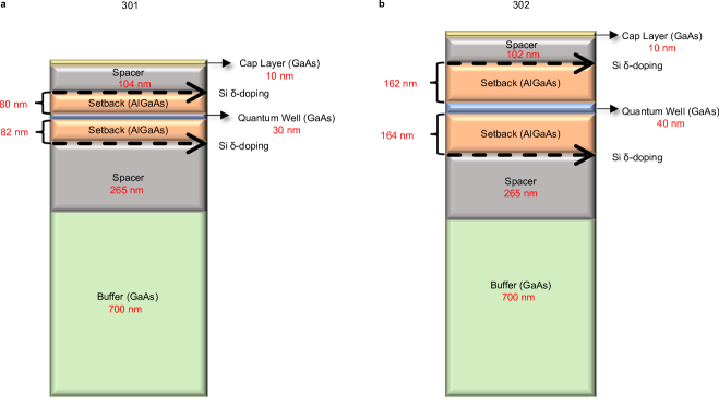
Experimental design and procedure. The measurements were performed on GaAs/AlGaAs symmetrically-doped heterostructures with a quantum well width of 30 (CBM301, VdP301) and 40 (CBM302, VdP302. A sketch of the heterostructure that include the main growth parameters such as the setback distances for the dopants and the capping layer thickness is provided in the SM for both samples. The electron density of CBM301 and VdP301 is , and for CBM302 and VdP302 is , as determined by magneto-transport measurements of Shubnikov de-Haas (SdH) oscillations at low magnetic fields, see SM. Their mobilities are and , respectively.
The electrical contacts for the Corbino samples were patterned using UV lithography followed by e-beam deposition of Ge/Au/Ni/Au layers of thickness and at a rate. Subsequently, the contacts were annealed in H2N2 atmosphere using a two step annealing procedure: a first step at followed by a longer step at Ben2015 ; Bennaceur2018 .
Both Corbino samples have three 2DEG rings with inner/outer radii , , and , respectively, see FIG.1(a). One van der Pauw sample was cleaved from the exact same wafer used to fabricate CBM302, and from a twin wafer with an identical heterostructure grown on the same day for CBM301. They are 3 3 mm square wafers with eight diffused indium contacts around the perimeter. All samples were cooled to a base temperature of approximately 20 in a dilution refrigerator, and were illuminated by a red LED from room temperature down to approximately 6 to increase both the mobility and density of the 2DEG. Specific details pertaining to the circuit used to perform the transport measurements are provided in the SM.
V Data availability
The data presented in this work are available from the corresponding author upon reasonable request.
VI Acknowledgments
This work has been supported by NSERC (Canada), FRQNT-funded strategic clusters INTRIQ (Québec), PromptInnov/MEI PSR Quantique (Québec) in partnership with Mitacs and Montreal-based CXC. The work at Princeton University is funded in part by the Gordon and Betty Moore Foundation’s EPiQS Initiative, Grant GBMF9615 to L. N. Pfeiffer, and by the National Science Foundation MRSEC grant DMR 2011750 to Princeton University. Sample fabrication was carried out at the McGill Nanotools Microfabrication facility. We would like to thank B.A. Schmidt and K. Bennaceur for their technical expertise during the fabrication and the earlier characterization of the Corbino sample, and R. Talbot, R. Gagnon, and J. Smeros for general laboratory technical assistance.
VII Authors contributions
S.V. and G.G. conceived the experiment. K.W.W. and L.N.P. performed the semiconductor growth by molecular beam epitaxy and provided the material. S.V. fabricated the Corbino and prepared the VdP samples. S.V. performed the electronic transport measurement in the Corbino samples at low temperatures, with the assistance and expertise of F.P. and M.P. O.Y. assisted in noise reduction and pre-amplification. S.V. performed the data analysis, helped by Z.B.K. for the development of computer routine. M.P.L. and T.S. provided important expertise regarding data acquisition, semiconductor expertise, and interpretation of the results. K.A. provided theoretical guidance. S.V. and G.G, wrote the manuscript, and all authors commented on it.
Competing interests : The authors declare no competing interests.
Corresponding author information : Guillaume Gervais, gervais@physics.mcgill.ca.
References
- (1) Chung, Y. J., Gupta, A., Baldwin, K. W., West, K. W., Shayegan, M. and Pfeiffer, L. N. Understanding limits to mobility in ultrahigh-mobility GaAs two-dimensional electron systems: 100 million and beyond, Phys. Rev. Lett. 106, 075134 (2022).
- (2) Gurzhi, R. N., Minimum of resistance in impurity-free conductors, Sov. Phys. JETP 17, 521 (1963).
- (3) Gurzhi, R. N., Hydrodynamic effects in solids at low temperature, Sov. Phys. Usp. 11, 255 (1968).
- (4) Ahn, Seongjin and Das Sarma, Sankar, Hydrodynamics, viscous electron fluid, and Wiedeman-Franz law in two-dimensional semiconductors, Phys. Rev. B 106, L081303 (2022).
- (5) Umansky, V., de-Picciotto, R. and Heiblum, M., Extremely high-mobility two dimensional electron gas: Evaluation of scattering mechanisms, Appl. Phys. Lett. 71, 683 (1997).
- (6) Casimir, H. B. G., reciprocity theorems and irreversible processes, IEEE 51, 1570 (1963).
- (7) Beauchamp, C. B., Dimitriadis, S., Nicholls, J. T., Levitin, L. V., Casey, A. J., See, P., Creeth, G., Waldie, J., Farrer, I., Beere, H. E. and Ritchie, D. A., Superconductivity in AuNiGe Ohmic contacts to a GaAs-based high mobility two-dimensional electron gas, Appl. Phys. Lett. 117, 162104 (2020).
- (8) Levitin, L. V., Theisen, T., Dimitriadis, S., Lucas, M., Corcoles, A. D., Nyéki, J., Casey, A. J., Creeth, G., Farrer, I., Ritchie, D. A., Nicholls, J. T. and Saunders, J., Cooling low-dimensional electron systems into the microkelvin regime, Nat. Commun. 13, 1-8 (2022).
- (9) Hwang, E. H. and Das Sarma, S., Limit to two-dimensional mobility in modulation-doped GaAs quantum structures: How to achieve a mobility of 100 million, Phys. Rev. B 77, 235437 (2008).
- (10) Savard, M., Tremblay-Darveau, C. and Gervais,G., Flow conductance of a single nanohole, Phys. Rev. Lett. 103, 104502 (2009).
- (11) Gooth, J., Menges, F., Kumar, N., Shekhar, C., Sun, Y., Drechsler, U., Zierold, R., Felser, C. and Gotsmann, B.,Thermal and electrical signatures of a hydrodynamic electron fluid in tungsten diphosphide, Nat. Commun. 9, 4093 (2018).
- (12) W. Moll, P. J., Kushwaha, P., Nandi, N., Schmidt, B., and Mackenzie, A. P., Evidence for hydrodynamic electron flow in PdCoO2, Science 351, 1061 (2016).
- (13) de Jong, M. J. M. and Molenkamp, L. W., Hydrodynamic electron flow in high-mobility wires, Phys. Rev. B 51, 13389 (1995).
- (14) Gusev, G. M., Jaroshevich, A. S., Levin, A. D., Kvon, Z. D. and Bakarov, A. K., Viscous magnetotransport and Gurzhi effect in bilayer electron system, Phys. Rev. B 103, 075303 (2021).
- (15) Kumar, A. S., Liu, C., Liu, S., Pfeiffer, L. N., West, K. W., Levchenko, A., and Gao, X. P., Interaction effects and viscous magneto-transport in a strongly correlated 2D hole system, arXiv:2105.06502v1.
- (16) Gusev, G. M., Levin, A. D., Levinson, E. V. and Bakarov, A. K., Viscous electron flow in mesoscopic two-dimensional electron gas, AIP Adv. 8, 025318 (2018).
- (17) Gupta, A., Heremans, J. J., Kataria, G., Chandra, M., Fallahi, S., Gardner, G. C. and Manfra, M. J., Hydrodynamic and Ballistic Transport over Large Length Scales in , Phys. Rev. Lett. 126, 076803 (2021).
- (18) Keser, A. C., Wang, D. Q., Klochan,O., Ho, D. Y. H., Tkachenko, O. A., Tkachenko, V. A., Culcer, D., Adam, S., Farrer, I., Ritchie, D. A., Sushkov, O. P., and Hamilton, A. R., Geometric control of universal hydrodynamic flow in a two-dimensional electron fluid, Phys. Rev. X 11, 031030 (2021).
- (19) Krishna Kumar, R.,Bandurin, D. A., Pellegrino, F. M. D., Cao, Y., Principi, A., Guo, H., Auton, G. H., Ben Shalom, M., Ponomarenko, L. A., Falkovich, G., Watanabe, K., Taniguchi, T., Grigorieva, I. V., Levitov, L. S., Polini, M.and Geim, A. K., Superballistic flow of viscous electron fluid through graphene constrictions, Nat. Phys. 13, 1182-1185 (2017).
- (20) Bandurin, D. A., Shytov, A. V., Levitov, L. S., Kumar, R. K., Berdyugin, A. I., Ben Shalom, M., Grigorieva, I. V., Geim, A. K. and Falkovich, G., Fluidity onset in graphene, Nat. Commun. 9, 4533 (2018).
- (21) Ku, M. J., Zhou, T. X., Li, Q., Shin, Y. J., Shi, J. K., Burch, C., Anderson, L. E., Pierce, A. T., Xie, Y., Hamo, A., Vool, U., Zhang, H., Casola, F., Taniguchi, T., Watanabe, K., Fogler, M. M., Kim, P., Yacoby, A., and Walsworth, R. L., Imaging viscous flow of the Dirac fluid in graphene, Nat. Phys. 583, 537-541 (2020).
- (22) Jenkins, A., Baumann, S., Zhou, H., Meynell, S. A., Daipeng, Y., Watanabe, K., Taniguchi, T., Lucas, A., Young, A. F., and Bleszynski Jayich, A. C., Imaging the breakdown of Ohmic transport in graphene, Phys. Rev. Lett. 129, 087701 (2022).
- (23) Kumar, C., Birkbeck, J., Sulpizio, J. A., Perello, D., Taniguchi, T., Watanabe, K., Reuven, O., Scaffidi, T., Stern, A., Geim, A. K., and Ilani, S., Imaging hydrodynamic electrons flowing without Landauer–Sharvin resistance, Nature 609, 276-281 (2021).
- (24) Shavit, M., Shytov, A. and Falkovich, G., Freely flowing currents and electric field expulsion in viscous electronics, Phys. Rev. Lett. 123, 026801 (2019).
- (25) Li, Songci , Levchenko, A. and Andreev, A. V., Hydrodynamic thermoelectric transport in Corbino geometry, Phys. Rev. B 105, 125302 (2022).
- (26) Levchenko, A., Li, Songci and Andreev, A. V., Hydrodynamic magnetoresistance in graphene Corbino devices, Phys. Rev. B 106, L201306 (2022).
- (27) Narozhny, Boris N., Hydrodynamic approach to two-dimensional electron systems, Riv. Nuovo Cim. 45, 661–736 (2022).
- (28) Chung, Yoon Jang, Baldwin, K. W., West, K. W., Haug, N., van de Wetering, J., Shayegan, M. and Pfeiffer, L. N., Spatial mapping of local density variations in two-dimensional electron systems using scanning photoluminescence, Nano Lett. 19, 1530-6984 (2019).
- (29) Avron, J. E., Seiler, R. and Zograf, P. G., Viscosity of quantum Hall fluids, Phys. Rev. Lett. 75, 697-700 (1995).
- (30) Holder, T., Queiroz, R. and Stern, A., Unified description of the classical Hall viscosity, Phys. Rev. Lett. 123, 106801 (2019).
- (31) Schmidt,B. A., Bennaceur, K., Bilodeau,S., Gervais, G., Pfeiffer, L. N., and West, K. W.,Second Landau level fractional quantum Hall effects in the Corbino geometry, Solid State Communications 217, 1 (2015).
- (32) Bennaceur, K. and Lupien, C. and Reulet, B. and Gervais, G. and Pfeiffer, L. N. and West, K. W., Competing Charge Density Waves Probed by Nonlinear Transport and Noise in the Second and Third Landau Levels, Phys. Rev. Lett.,120 136801(2018)
Supplementary Material
VIII Heterostructure
A sketch of the wafer heterostructure used to fabricate CBM301, VdP301 and CBM302, VdP302 is shown in Fig.S1. The main components forming the heterostructure grown on an undoped GaAs subtrate are: a buffer/spacer, the setback defining the position of the dopants, the quantum well width, and the spacer/capping layer. The main differences between the 301 and 302
heterostructures are: the electron density ( for CBM301 and for CBM302); the quantum well width (30 for CBM301 and 40 for CBM302); the setback distance for the dopants (80 for CBM301 and 160 for CBM302).
IX Electronic transport measurement circuit
In the main text of the manuscript, Fig.2 shows the conductance of Corbino devices measured with two different electrical setups, and these are discussed below.
IX.1 Experimental setup A
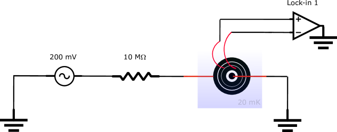
The experimental setup A shown in Fig.S2 consists of a SR830 lock-in amplifier and a resistor with a high resistance. An output voltage of 200 is passed through a 10 resistor connected in series with the Corbino device. This configuration allows us to apply a constant current of 20 to the outermost contact of the Corbino while keeping the inner contact grounded. The four-point resistance is calculated from the voltage drop measured across the inner two rings of the Corbino samples.
IX.2 Experimental setup B
In the Corbino geometry, the sample has a large magneto-resistance in non-zero magnetic fields, which makes the previous experimental setup not ideal for this case. Experimental setup B was used to measure the conductance while sweeping the magnetic field in order to extract the electron density from the Shubnikov de-Haas (SdH) oscillations. In this configuration, an output voltage of 100 was applied to a voltage divider consisting of 100 100 , connected in series with the Corbino. The current through the sample is calculated from the measured voltage drop across a 1 resistor connected in series with the Corbino. For both experimental setups A and B, a voltage pre-amp with the gain of 100 was used at the output end.

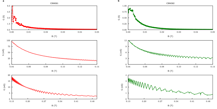
X Magneto-transport measurement
In Fig.S4 the magneto-conductance measured at low perpendicular magnetic fields with the experimental setup B and is shown. The onset of Shubnikov-de Haas oscillations (SdH) is observed at very low magnetic fields as expected from the very high electron mobility of the 2DEGs. Due to a large magneto-conductance at low magnetic field in a Corbino sample, distinct panels show the conductance over different magnetic field ranges. No evidence was found for a superconducting transition, i..e a superconducting critical field, in either samples.
XI Electron density extraction
The SdH oscillations (after reducing the background) of conductivity (or conductance) versus inverse magnetic field are given by,
| (S1) |
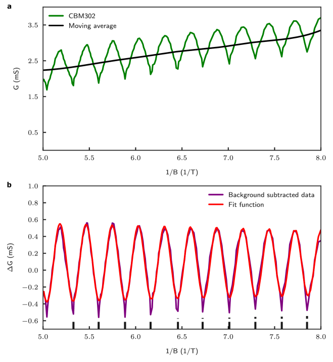
where the and is the SdH frequency. Here, we use the conductivity and conductance terms interchangeably since both parameters are related via a simple geometric factor. Fig.S5 shows the background reduced SdH data and the fit performed for CBM302 at 20 . In it, we used the moving average of the raw data which was then subtracted to obtain the background reduced SdH oscillations. The fitting function used Eq S1 to obtain the SdH frequency which was then used to calculate the electron density ,
| (S2) |
where and are the electron charge and Planck’s constant.
XI.1 Temperature dependence of electron density
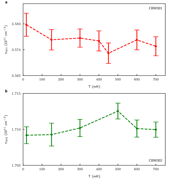
The electron density extracted using the aforementioned procedure at different temperatures ranging from 20 to 750 for CBM301 and CBM302 are shown in Fig.S6. The calculated electron density remains constant within in the temperature interval where the anomalous behaviour in electronic transport was observed.
XII Data consistency and reproducibility
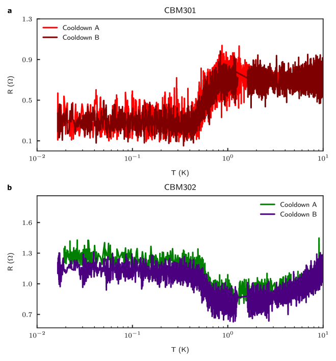
The anomalous behavior in resistance observed in CBM301 and CBM302 has been reproduced during several cooldowns. Fig.S7 shows the data obtained for two different cooldowns in the same dilution refrigerator system using experimental setup A for both Corbino samples. In addition to the data shown in Fig.S7, the results have been reproduced several times using both experimental setups in different cooldowns, and also in two different dilution refrigerators with distinctive electronics.
XIII Transport measurements at higher temperature
Electronic transport measurements were also performed at higher temperatures than shown in the main text, and they are shown in Fig.S8. As expected, the monotonic increase in resistance with increasing temperature for VdP301 and VdP302 is observed. Note the increase in resistance observed at 400 for CBM301 is followed by a nearly-constant resistance value over a wide range of temperature up to 10 K, and subsequently a monotonic increase in resistance is observed at higher temperatures.