Dynamics and Resilience of the Charge Density Wave in a Bilayer Kagome Metal
Abstract
Long-range electronic order descending from a metallic parent state constitutes a rich playground to study the intricate interplay of structural and electronic degrees of freedom Neupert_2022 ; Arachchige_2022 ; Wang_2021a ; Heumen_2021 ; Luo_2022 . With dispersive and correlation features as multifold as topological Dirac-like itinerant states, van-Hove singularities, correlated flat bands, and magnetic transitions at low temperature, kagome metals are located in the most interesting regime where both phonon and electronically mediated couplings are significant Kang_2020 ; Kang_2020b ; Lin_2018 ; Ye_2019 ; Pokharel_2021 ; Hu_2022 . Several of these systems undergo a charge density wave (CDW) transition, and the van-Hove singularities, which are intrinsic to the kagome tiling, have been conjectured to play a key role in mediating such an instability. However, to date, the origin and the main driving force behind this charge order is elusive. Here, we use the topological bilayer kagome metal ScV6Sn6 as a platform to investigate this puzzling problem, since it features both kagome-derived nested Fermi surface and van-Hove singularities near the Fermi level, and a CDW phase that affects the susceptibility, the neutron scattering, and the specific heat Arachchige_2022 , similarly to the siblings V3Sb5 ( = K, Rb, Cs) Neupert_2022 ; Kang_2023 and FeGe Teng_2022 . We report on our findings from high—resolution angle-resolved photoemission, density functional theory, and time-resolved optical spectroscopy to unveil the dynamics of its CDW phase. We identify the structural degrees of freedom to play a fundamental role in the stabilization of charge order. Along with a comprehensive analysis of the subdominant impact from electronic correlations, we find ScV6Sn6 to feature an instance of charge density wave order that predominantly originates from phonons. As we shed light on the emergent phonon profile in the low-temperature ordered regime, our findings pave the way for a deeper understanding of ordering phenomena in all CDW kagome metals.
** These authors contributed equally
Bilayer kagome metals are an emerging class of correlated topological compounds with chemical formula V6Sn6 (: rare earth - hereafter also dubbed as the 166 family), featuring unconventional topological phases and collective magnetic excitations at low temperature Pokharel_2021 ; Hu_2022 ; Arachchige_2022 ; Peng_2021 ; Ishikawa_2021 ; Rosenberg_2022 ; Lee_2022 ; Chen_2021 . Similarly to the sister compounds V3Sb5 (: alkali atoms - hereafter also nicknamed as the 135 family), the electronic structure of V6Sn6 is a rich platform for the emergence of unconventional phase diagrams, boasting the simultaneous presence of itinerant Dirac electrons, non-trivial flat bands, and van-Hove singularities at the Fermi energy Kang_2020 ; Kang_2020b ; Lin_2018 ; Ye_2019 ; Guo2009 ; Mazin2014 ; Kiesel2013 ; DiSante2020 ; Neupert_2022 . Among the 166 family, ScV6Sn6 exhibits a unique three-dimensional charge density wave (CDW) transition, with a motif dissimilar to those observed in other kagome compounds Kang_2023 . Here, the CDW phase provokes a weak atomic lattice displacement, which might generate unconventional phenomena, such as metal-insulator transitions of fermions, vortexes at the surface, chiral currents, and bond orders Arachchige_2022 ; Guo_2022 ; Nishimoto_2010 ; Kiesel_2013 ; Denner_2021 ; Feng_2021 ; Park_2021 ; Jiang_2021 ; Liang_2021 . The major goal of contemporary research thus is to reveal the underlying mechanism of the charge order in ScV6Sn6 and the specific role of structural and electronic degrees of freedom, the interdependence of whom has so far remained uncharted territory.
Previous works have highlighted important differences between the CDW in ScV6Sn6, V3Sb5, and FeGe Teng_2022 . In V3Sb5, the charge order has been thought to be connected to the nesting of the Fermi surface, exemplified by the van-Hove singularity electron filling Wu2021 ; Kang2022 ; Ortiz2020 ; Kang_2023 . In these systems, the charge order has been conjectured to be linked to the emergence of superconductivity and stripe orders Yu_2021 ; Liang_2021 ; Du_2021 ; Oey_2022 ; Li_2021a ; Wang_2021b ; Zhao_2021 . In addition, the atomic displacement following the onset of the CDW involves mostly the V atoms and their in-plane positions. ScV6Sn6, surprisingly, does not undergo any superconducting transition at low temperature and the motif of the CDW, generated by the ordering vector , does not give rise to either the Star of David or trihexagonal arrangement, as for the V3Sb5 compounds, for which the ordering vectors are and Ortiz_2021 ; Ortiz2020 ; Nie_2022 . This is ascribed to the involvement of Sn and Sc atoms in the lattice modulation. The differences between these two systems, are also reflected in a much more rapid CDW suppression for ScV6Sn6 under the application of pressures Zhang_2022 , offering an increased ease of tuneability compared to V3Sb5.
In CDW materials, the simultaneous occurrence of a lattice displacement and a change in the electronic structure, often associated with the opening of gaps in the electronic spectrum challenges the understanding of the main driving force behind the charge order and limits the access to possible consequent or concomitant cascade of collective phases and their control. While there is compelling evidence of CDW in kagome systems, its microscopic origin and dynamics are still debated. We stress that the understanding of such origin and dynamics is a task of paramount importance given the peculiar electronic structure of kagome with van-Hove singularities at the Fermi level and the presence of a nested Fermi surface, which hints at an energy gain upon a gap opening as an underlying driver. For 166, which has also a topological nature, it becomes crucial to understand the dynamics of the CDW, to uncover not only the relationship between subsequent ordered phases, but to elucidate the interplay between phase transition and electron spins Hu_2022 ; Yin_2022 ; Sun_2022 ; Tanaka_2020a ; Ortiz2020 ; NagaosaPRB2019 . In the present study, we used time-resolved optical spectroscopy (TR-OS) to unveil the dynamics of the CDW in the 166 bilayer kagome ScV6Sn6. Specifically, by using TR-OS, we disclose the energy scales involved in the charge order, which points towards a major robustness of the lattice degree of freedom for the observed transition.
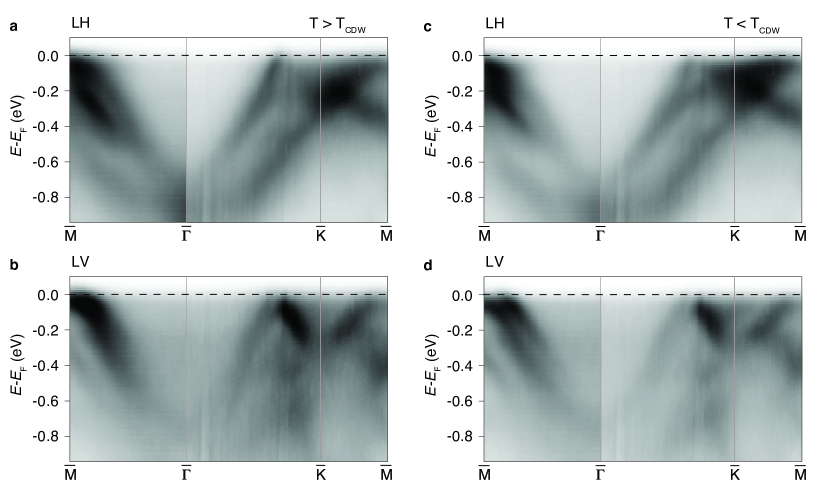
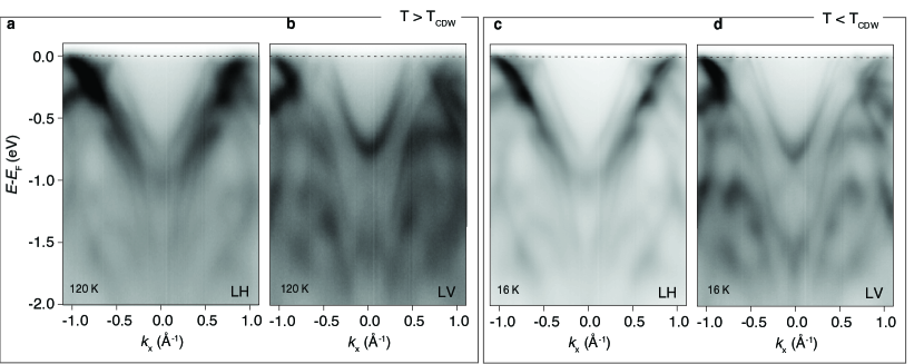
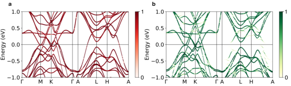
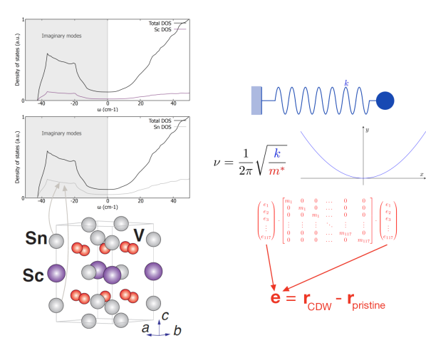
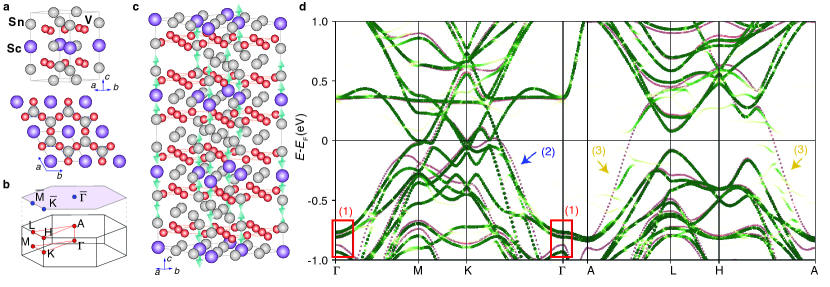
First, we describe the electronic properties of ScV6Sn6, then we will show by using ARPES, DFT, and TR-OS how the electronic and structural degrees of freedom are affected by the CDW order. Along with the crystal structure (both with and without CDW) and the Brillouin zone (Figs.1 a-b), we show the expected electronic structure from density functional theory (DFT), above and below the transition temperature, in Fig.1 c (red color without CDW, green shades with CDW). In both CDW and pristine cases, the Dirac-like states and the van-Hove singularities are similar and identifiable, with negligible variation in their electronic dispersion along the -K-M- path. According to the calculations, the van-Hove singularities are located around the Fermi level. It is thus noteworthy that large changes at EF are not seen upon inclusion of the CDW nested systems Whangbo_1991 ; Carpinelli_1996 ; Tam_2022 ; Bosak_2021 . Along the -K-M- high-symmetry direction, the main changes occur at the point within the energy window [-0.75, -1] eV. Below the transition temperature, the separations between the bands increase by approximately 30 meV compared to the electronic structure without CDW (see red box in Fig.1 c). Other changes along the same direction, even if smaller, are indicated by the blue arrows (labeled as ’2’). If in the plane that comprises the point, the changes are rather subtle, our DFT calculation reveals that the CDW has its major effect along the A-H and A-L directions (see yellow arrows labeled as ’3’). There, we notice that the charge order opens several energy gaps along the entire -space path. Nonetheless, we also notice that the spectral weight immediately fades away from the gap openings. In addition, the spectral intensity in the CDW phase is still located around the poles of the electronic structure of the bands above . As a result, the gaps themselves are expected to be challenging to detect experimentally given the vicinity to the poles, the broadening, and the experimental resolution ( 15 meV, that is larger than the gap value itself) Sunko_2020 .
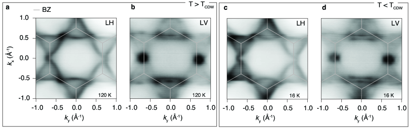
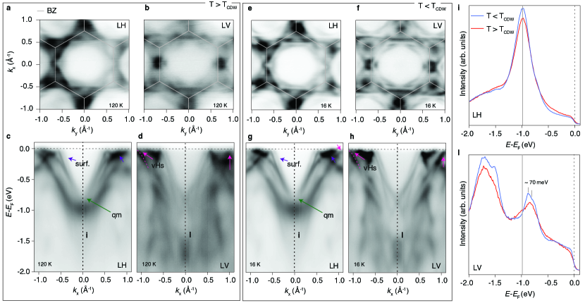
Similarly to other 166 materials, as shown in Fig. 2, ScV6Sn6 shows the presence of surface states, after the ultrahigh vacuum (UHV) cleave (see Methods for details about the samples’ preparation). These surface states have been extensively discussed for other kagome systems Kang2022 ; Kang_2020 ; Kang_2020b and members of the 166 family Pokharel_2021 ; Peng_2021 ; Ishikawa_2021 ; Rosenberg_2022 ; Hu_2022 . While they offer an interesting platform for exploiting spin-momentum locking because of their non-trivial topology Hu_2022 ; Li_2014 ; Li_2018 ; Jiang_2016 ; Luo_2017 , they could challenge the clear visualization of small changes occurring in the bulk electronic structure as a consequence of the charge order, because they could obfuscate subtle spectroscopic features. Thus, to exclude this avenue, we measured the electronic structure above and below the transition temperature and along the -K-M- high symmetry direction, with and without surface states such that one can better distinguish the bulk from the surface-derived signal (see Fig.2 for the clean surface case with both light polarizations and Supplementary Information Figs. 1 and 2 for data where the surface states have been suppressed and how). Along the selected high-symmetry path, we have the most favorable photoemission matrix elements and the intensity of the bands is the most prominent. Notably, no remarkable differences are observed across , besides a constant thermal broadening which affects the spectra collected above .
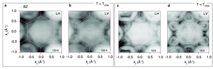
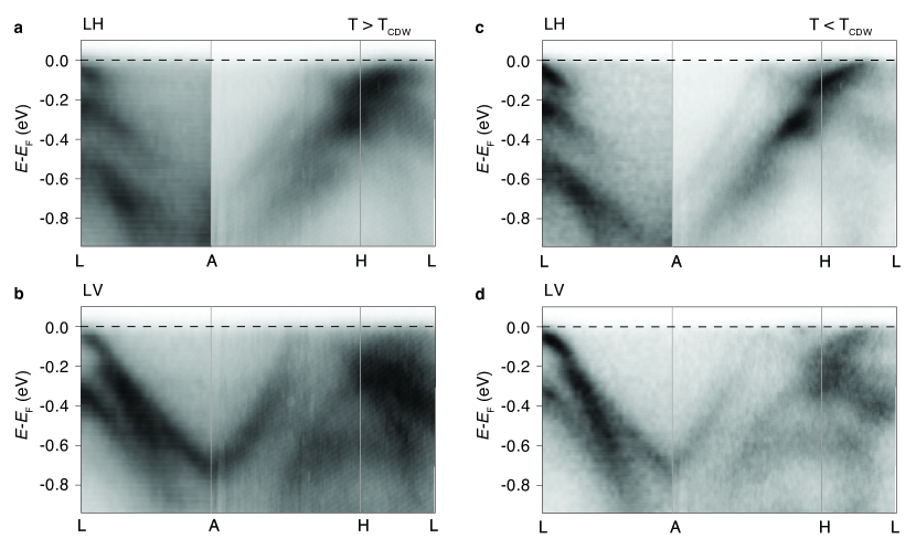
To still check possible effects of the charge order, from the ARPES spectra collected along the -K-M- path, we extracted energy-distribution curves (EDCs) across the point, where we expect the strongest changes induced by the CDW (Fig.2 i-l and red box of Fig.1 c). By using linear-horizontal (LH) polarized light, it is hardly possible to see the relevant states affected by the charge order (see Fig.2 i). By using linear-vertical (LV), instead, the missing spectral weight is recovered. In this condition, we resolve a 70 meV splitting at approximately eV of binding energy. Such a splitting might be consistent with the calculated increase in the energy separation produced by the CDW, however, we cannot exclude that this might be an effect of the band sharpening due to the lower temperature (see Fig.2 l). Despite having weaker intensity due to photoemission matrix elements, we also collected ARPES spectra along the A-L and A-H high-symmetry directions (shown in Supplementary Information Figs. 3, 4, and 5). Along these paths, the DFT analysis predicts the strongest changes in the electronic structure. Unfortunately, the changes from above to below are very small and not well-resolved experimentally. This is likely due, as anticipated above, to the combination of broadening, finite experimental resolutions, small energy values of the gaps, and expected spectral weight concentrated along the poles of the bands above the CDW transition.
The ARPES data depict a situation where most of the electronic spectral weight is only weakly affected by the CDW order in the proximity of the Fermi level (within the experimental resolutions). This is in line with DFT only showing a partial gap opening, which involves only certain bands but not the majority of the V-derived spectral weight. In addition, the partial gap calculated in the electronic structure agrees well with recent optical measurements in the static regime performed for ScV6Sn6, which show a sharp first order transition without the development of full gaps in the optical spectra Arachchige_2022 . Importantly, this behaviour describes a rather rare phenomenology, which is different from the most commonly observed second-order density condensation gaps, found in systems which undergo a CDW transition. In other words, the inability to spectroscopically resolve changes in the Fermi surfaces across the transition temperature makes ScV6Sn6 reminiscent of the CDW behaviour discovered for IrTe2 , TaTe2, and BaNi2As2 Li_2014b ; Hu_2022 ; Fang_2013 . This aspect is intimately related to the underlying electronic structure of the compound; the vanadium states indeed contribute in a significant way to the density of states around , while the corresponding atoms are not influenced by the CDW displacement. Conversely, tin and scandium states are not predominant at while the corresponding atoms’ positions are particularly influenced by the CDW transition. Additionally, ScV6Sn6 shows a very peculiar ordered phase, with a marked peak in the specific heat and an increased metallic character below the transition Arachchige_2022 . However, the origin of the charge order is still an open question. It is then crucial to separate the time- and energy-scales of the electronic and lattice degrees of freedom and to determine their robustness and involvement in the CDW order.
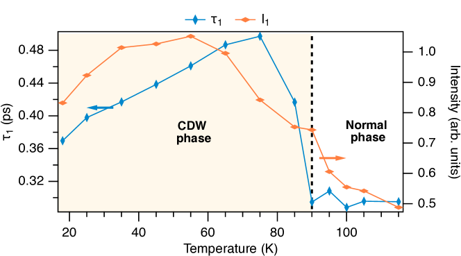
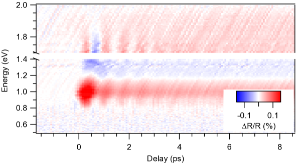
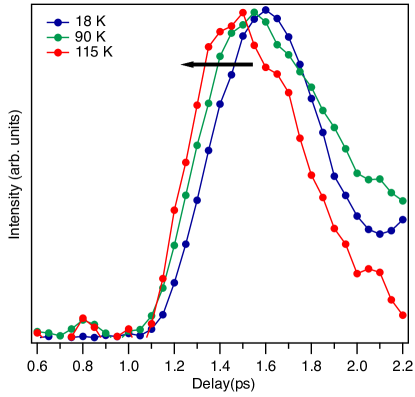
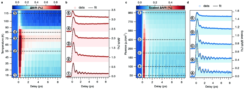
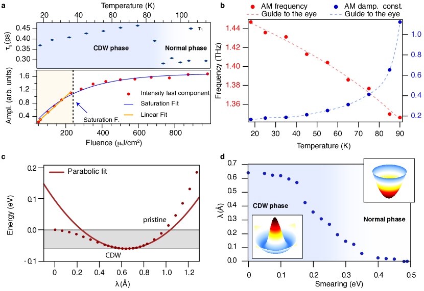
To this aim, we use TR-OS and we measure the time-resolved reflectivity dynamics of ScV6Sn6. Fig.3 a presents the temperature (T) dependence of the photoinduced reflectivity transients, , recorded upon increasing the temperature (T from approximately 18 K; the fluence was F 0.2 mJ/cm2). The can be described by two features: an incoherent (non-oscillating) response and a coherent oscillatory behaviour. In our data, clear oscillations in the , showing a strong T-dependence, are detected up to the transition temperature (Fig.3 a-b). The incoherent (non-oscillating) response consists of two decays, a fast and a slow one, with characteristic times and , respectively (see Supplementary Information for details about the data analysis and their extraction) that appear in the data as a fast peak and a slowly-decaying component. Similarly to the coherent response, the incoherent one is also strongly T-dependent and it shows the indication of a phase transition around T 90 K (see Fig.4 a), which matches well with the nominal Arachchige_2022 . Above , the becomes smaller and, after the fast exponential decay, it changes sign becoming negative (see trace ’5’ of Fig.3 b).
In general, below the critical CDW temperature, the pump pulse induces an abrupt change in the reflectivity, followed by a fast decay within a picosecond and a slower recovery on a timescale of the order 10 ps Tomeljak_2009 ; Yusupov_2008 ; Pokharel2022 ; Vorobeva_2011 ; Ravnik_2018 . The first, which slows down critically upon approaching the transition temperature, is attributed to the re-opening of the CDW gap, while the second one, as confirmed by detailed studies of the dynamics as a function of the excitation fluence and applied external electric field, is attributed to a second stage of the CDW recovery Eichberger2010 ; TOMELJAK2009_physB ; Huber_2014 ; Storeck_2020 .
In ScV6Sn6, the T-evolution of the incoherent part of the shows a rather peculiar behavior: in contrast to the well-studied one dimensional CDW systems, the lifetime of the first fast decay increases linearly with the temperature and shows a rapid drop at (Fig.4 a). Remarkably, no divergence of the lifetime is observed during the phase transition. This peculiar behavior, in combination with our ARPES measurements and DFT analysis, suggests an unusual origin for the CDW phase in this material, where no gaps are observed in the near Fermi level region. Indeed, a divergence of the lifetime is usually linked to the closing of the electronic gap that develops in conventional CDW transitions. This is also different from what has been observed in the kagome metal CsV3Sb5, where TR-OS measurements have highlighted the divergence of the lifetime of the fast decay process during the onset of the charge order Wang_2021b .
Interestingly, from the fits to the data (see Supplementary Information for more details), the frequency of the oscillatory mode and the damping show a pronounced temperature dependence, as we show in Fig.4 b. In particular, at low temperature the mode is characterized by a frequency of 1.45 THz, in excellent agreement with our ab-initio estimate of 1.42 THz from the quadratic fit of the DFT total energy around the minimum of CDW ordered structure (see Fig.4 c and Methods for more details), and we observe a 6 softening of the mode frequency and an exponential increase of the damping constant, when the temperature of the system approaches the critical temperature of the CDW transition. Such a temperature dependence has been observed in many CDW systems and it constitutes the fingerprint of an amplitude mode (AM) of the CDW phase Demsar_1999 ; Chen_2017 ; Yusupov2010 ; Yoshikawa2021 ; Vorobeva_2011 ; Ravnik_2018 . This observation confirms that the coherent response is not due to a trivial phonon, but rather to the excitation of the AM of the CDW phase, confirming the onset of CDW physics in ScV6Sn6. We also note that no fingerprints of an AM have been hitherto detected in CsV3Sb5 by previous reflectivity studies Wang_2021b .
By varying the excitation density (fluence), additional information about the nature of the phase transition can be obtained. The melting of electronic modulation is generally achieved on a timescale much faster than the characteristic timescale related to the relaxation of the periodic lattice modulation, which is given by the period of the characteristic amplitude modes of the system. This results in the disentanglement of electronic and lattice degrees of freedom on the sub-picosecond time scale, with a subsequent rapid recovery of the electronic degrees of freedom Schaefer2013 ; Yusupov2010 ; Vorobeva_2011 ; Stojchevska_2011 . Additionally, the characteristic energy required to fully drive the phase transition, i.e. quenching the periodic lattice distortion and the electronic degrees of freedom, is that one which leads to the disappearance of the (oscillatory) amplitude mode Pokharel2022 ; Schaefer2013 . This provides a means to quantify the strength of the lattice degree of freedom compared to the electronic one. We report this in Fig. 3 c, where the evolution of the scaled signal as a function of the fluence is shown, in a range from to J/cm2. The traces are scaled to the fluence to better visualize the qualitative behavior of the response upon approaching the photoinduced phase transition. Note that the sample is kept at a temperature well-below . In the low perturbation regime, the signal scales linearly with excitation density (traces A, B, C in Fig. 3 d), while upon approaching the photoinduced phase transition the signal related to CDW order shows saturation Schaefer2013 ; Pokharel2022 .
The maximum change that can be induced in the signal is generally achieved when the electronic degree of freedom associated to the CDW order is collapsed. We find that the fast electronic component with relaxation time saturates at a fluence, where the oscillations linked to AM involving the lattice degrees of freedom persist Schaefer2013 ; Tomeljak_2009 ; Pokharel_2022 . By progressively increasing the excitation fluence, the oscillations in the due to the AM get also suppressed, with an exponential increase of the damping constant and a softening of the frequency of the mode. Remarkably, our measurements highlight the robustness of the lattice reconstruction of the CDW in this material. Indeed, even at high excitation fluences (J/cm2), the oscillations due to the AM are still detected. This behavior is again markedly different from what has been observed in the sister compound CsV3Sb5, where already at a pump fluence as small as J/cm2, the CDW order is melted Wang_2021a . In our study, we show that the oscillation disappears completely only at a fluence of J/cm2, meaning that the lattice order can be melted, although at a fluence larger than the one required to saturate the purely electronic response at around 240 J/cm2. The electronic states that maximally couple to this CDW span an energy window around the Fermi level of about 0.25 eV, because smearing over that window greatly affects the AM, as we show in Fig. 4 d. Indeed, taking into account the electronic specific heat of ScV6Sn6, an absorbed fluence of 240 J/cm2 leads to an increase of the electronic temperature of 2100 K, which is in reasonable agreement with the smearing obtained by DFT calculations (See Fig. 4 d). Finally, it is only when the average lattice temperature exceeds the CDW critical temperature because of the average power deposited by the pump pulse, that one might expect to detect the transient signal of the high-temperature phase. We estimate the pump-induced average heating to be in a 20 K at a fluence of 1 mJ/cm2. Hence, in order to reach , very large fluences are required, which are not attainable because sample damage would occurr.
In conclusion, by using the combination of experimental techniques, i.e. ARPES and TR-OS, as well as theoretical calculations, we disclose the dynamics of the unusual CDW transition in ScV6Sn6 and we simultaneously demonstrate marginal energy gaps at the Fermi level. In particular, temperature dependent TR-OS reveals the hallmarks of the CDW. In addition, our fluence dependent study disentangles the electronic and structural degrees of freedom, showing persisting AM oscillation up to unusually high values of fluence, corroborating the robustness of the lattice distortions compared to the sudden disruption of the purely electronic component. Such dynamics is in favor of a CDW with the lattice degrees of freedom and electron-phonon interaction playing the dominant role. We believe that our comprehensive study sheds light onto the collective modes emerging in the low-temperature phase of ScV6Sn6. It paves the way for the understanding of unconventional many-body phases in correlated kagome metals, which all share a similarly nested Fermi surface, and deepens our understanding of cooperative lattice and electronic symmetry breaking at this new frontier. Therefore, we think that our discovery is the crucial step to understand the origin and drive of the CDW also in the archetypal family AV3Sb5.
Methods
Experimental details –
Single crystals of ScV6Sn6 were grown using a flux-based growth technique as reported in the reference PhysRevMaterials.6.104202 . Sc (chunk, 99.9), V (pieces, 99.7), and Sn (shot, 99.99) were loaded inside an alumina crucible with the molar ratio of 1:6:20 and then heated at 1125 ∘C for 12 h. Then, the mixture was slowly cooled to 780 ∘C at a rate of 2 ∘C/h. Thin plate-like single crystals were separated from the excess Sn-flux via centrifuging at 780 ∘C. The samples were cleaved in ultrahigh vacuum (UHV) at the pressure of 110-10 mbar. The ARPES data were acquired at the APE-LE end station (Trieste) using a VLEED-DA30 hemispherical analyzer. The energy and momentum resolutions were better than 12 meV and 0.02 Å-1, respectively. The temperature of the measurements was kept constant throughout the data acquisitions (16 K and 120 K, below and above respectively). Both linear polarizations were used to collect the data from the APE undulator of the synchrotron radiation source ELETTRA (Trieste). The photon energy used for the ARPES data was 75 eV. This choice was such that the spectra intensity was the most prominent, especially near the region of the quadratic minimum of the electronic structure, where the major changes with the CDW are expected.
Time-resolved reflectivity experiments were performed at the T-ReX laboratory (FERMI, in Trieste) with a probe photon energy of 0.95 eV (1300 nm). The measurements were performed using a Ti:sapphire femtosecond (fs) laser system, delivering, at a repetition rate of 250 kHz, fs light pulses at a wavelength of 800 nm (1.55 eV). The single color probe measurements were performed at a probe wavelength of 1300 nm, obtained by filtering a broadband (0.8–2.3 eV) supercontinuum probe beam, generated using a sapphire window.
Theoretical details – DFT calculations have been performed using both Quantum Espresso and VASP packages. Phonon calculations are based on density functional perturbation theory, as implemented in Quantum Espresso doi:10.1063/5.0005082 ; Giannozzi_2009 ; Giannozzi_2017 . Exchange and correlation effects were included with the generalized gradient approximation (GGA) using the Perdew-Burke-Ernzerhof (PBE) functional PhysRevLett.77.3865 ; the pseudopotentials are norm-conserving and scalar relativistic, containing core corrections PhysRevB.88.085117 . Self-consistent calculations and ionic relaxation of the unit cell have been performed with a 996 -grid; convergence threshold for both ionic minimization and electronic self-consistency are set to be Ry. The kinetic energy cutoff for the wavefunctions is equal to 90 Ry. A ordinary Gaussian spreading of 0.006 Ry has been used. Once the structure was properly at equilibrium, with vanishing forces acting on each atom, we proceeded with the actual phonon calculations. The dynamical matrices have been obtained and computed for a -grid of 336, with a self-consistency threshold of Ry. These dynamical matrices are consequently Fourier-transformed to obtain the inter-atomic force constants (IFC) in real space; three translational acoustic sum rules have been imposed, via correction of the IFC. Finally, both phonon dispersion and phonon density of states are obtained. In particular, for the density of states calculations (see results in the Supplementary Information) we used 303030 -points. The presence of imaginary phonon modes has been verified also for a 669 and a 9912 -grid, during the dynamical matrices’ calculation.
The remaining DFT calculations have been performed with VASP. To study the dependence of the CDW phase with respect to the smearing we used a plane-wave cutoff of 500 eV and a 999 -centered -mesh. Ionic relaxations have been performed with a constant volume. The relaxations of the ionic and electronic degrees of freedom were considered converged respectively below a threshold of eV and eV. Subsequently, for each smearing value, we computed the norm of the 351-dimensional (117 atoms 3) displacement vector among the CDW and the pristine phases. Spin-orbit coupling has not been included for this set of calculations.
To study the structural interpolation among the CDW and pristine systems, leading to the double-well potential profile, we computed the 351-dimensional displacement vector between the two configurations. This has a norm of Å. The two structures hence are gradually interpolated, moving the atoms along the direction defined by . For each step, a self-consistent calculation with 500 eV for the kinetic energy cutoff and a -centered 121212 -grid has been performed. The smearing here is constant and equal to 0.005 eV. The electronic calculations are considered converged below a threshold of eV. This process has been studied while keeping the volume constant. Also here the spin-orbit coupling has not been included. To compute the frequency of the phonon mode we started from a quadratic fit around the minimum of the Born-Oppenheimer potential, corresponding to the CDW phase; the resulting fit has equation . From here it is possible to obtain the ”spring” constant , as 0.379202 eV/Å2. The effective mass is computed using the normalized displacement vector and the mass tensor diag(, , , …, , , ) via ; we obtain u. Note that this mass value is intermediate among the Sn and Sc ones, i.e. the atoms which mostly participate to the CDW transition. Finally the frequency can be computed as , with , giving us THz.
When considering the unfolding of the CDW supercell, the Kohn–Sham wave functions are expanded in plane waves up to a 400 eV energy cutoff, with a -mesh resolution for the self-consistent electronic structure calculations of 0.02 reciprocal Angstroms. For the non-self-consistent calculations, the -mesh resolution corresponds to 0.01 reciprocal Angstroms. In this case, the spin-orbit coupling has been considered and included self-consistently.
The initial CDW supercell corresponds in every case to the experimental one Arachchige_2022 . Band structures have been visualized using the VASPKIT postprocessing tool vaspkit . VESTA vesta has been used to visualize the crystal structures.
Acknowledgements
The authors acknowledge Andrea Cavalleri for the fruitful discussions on this work. The research leading to these results has received funding from the European Union’s Horizon 2020 research and innovation program under the Marie Skłodowska-Curie Grant Agreement No. 897276. We gratefully acknowledge the Gauss Centre for Supercomputing e.V. (https://www.gauss-centre.eu) for funding this project by providing computing time on the GCS Supercomputer SuperMUC-NG at Leibniz Supercomputing Centre (https://www.lrz.de). We are grateful for funding support from the Deutsche Forschungsgemeinschaft (DFG, German Research Foundation) under Germany’s Excellence Strategy through the Würzburg-Dresden Cluster of Excellence on Complexity and Topology in Quantum Matter ct.qmat (EXC 2147, Project ID 390858490) as well as through the Collaborative Research Center SFB 1170 ToCoTronics (Project ID 258499086) and the Hamburg Cluster of Excellence “CUI: Advanced Imaging of Matter” (EXC 2056, Project No. 390715994). This work has been performed in the framework of the Nanoscience Foundry and Fine Analysis (NFFA-MUR Italy Progetti Internazionali) facility. The Flatiron Institute is a division of the Simons Foundation. S.D.W. and G. Po. acknowledge support via the UC Santa Barbara NSF Quantum Foundry funded via the Q-AMASE-i program under award DMR-1906325. F.M. greatly acknowledges the SoE action of pnrr, number SOE_0000068. I.Z. acknowledges the support from U.S. Department of Energy (DOE) Early Career Award DE-SC0020130.
Author contributions
F.M., D.D.S and F.C. conceived and designed the project. G.Po. and S.W. grew the crystals. F.M., C.B., J.F., I.V., and P.C. carried out the ARPES measurements, while F.C., M.T., D.P., and W. B. obtained the pump and probe results. A.C. and S.E. performed the numerical calculations and theoretical analysis supervised by D.D.S, G.S., T.W. and R.T. All the authors participated in the discussion and crucially contributed to understanding and the writing of the manuscript.
Additional information
Extended data is available for this paper at https://xxxx
Supplementary information The online version contains supplementary material available at https://xxx
Correspondence and requests for materials should be addressed to Federico Mazzola, Domenico Di Sante and Federico Cilento.
Data availability The data that support the findings of this study are available from the corresponding authors upon reasonable request.
Competing financial interests
The authors declare no competing financial interests.
References
- (1) Neupert, T., Denner, M. M., Yin, J.-X., Thomale, R. & Hasan, M. Z. Charge order and superconductivity in kagome materials. Nature Physics 18, 137–143 (2022). URL https://www.nature.com/articles/s41567-021-01404-y.
- (2) Arachchige, H. W. S. et al. Charge density wave in kagome lattice intermetallic ScV6Sn6. Phys. Rev. Lett. 129, 216402 (2022). URL https://link.aps.org/doi/10.1103/PhysRevLett.129.216402.
- (3) Wang, Z. X. et al. Unconventional charge density wave and photoinduced lattice symmetry change in the kagome metal CsV3Sb5 probed by time-resolved spectroscopy. Phys. Rev. B 104, 165110 (2021). URL https://link.aps.org/doi/10.1103/PhysRevB.104.165110.
- (4) van Heumen, E. Kagome lattices with chiral charge density. Nature Materials 20, 1308–1309 (2021). URL https://www.nature.com/articles/s41563-021-01095-z.
- (5) Luo, H. et al. Electronic nature of charge density wave and electron-phonon coupling in kagome superconductor KV3Sb5. Nature Communications 13, 273 (2022). URL https://doi.org/10.1038/s41467-021-27946-6.
- (6) Kang, M. et al. Topological flat bands in frustrated kagome lattice CoSn. Nature Communications 11, 4004 (2020). URL https://www.nature.com/articles/s41467-020-17465-1.
- (7) Kang, M. et al. Dirac fermions and flat bands in the ideal kagome metal FeSn. Nature Materials 19, 163–169 (2020). URL https://www.nature.com/articles/s41563-019-0531-0.
- (8) Lin, Z. et al. Flatbands and emergent ferromagnetic ordering in Fe3Sn2 kagome lattices. Phys. Rev. Lett. 121, 096401 (2018). URL https://journals.aps.org/prl/abstract/10.1103/PhysRevLett.121.096401.
- (9) Ye, L. et al. de Haas-van Alphen effect of correlated Dirac states in kagome metal Fe3Sn2. Nature Communications 10, 4870 (2019). URL https://www.nature.com/articles/s41467-019-12822-1.
- (10) Pokharel, G. et al. Electronic properties of the topological kagome metals YV6Sn6 and GdV6Sn6. Phys. Rev. B 104, 235139 (2021). URL https://journals.aps.org/prb/abstract/10.1103/PhysRevB.104.235139.
- (11) Hu, Y. et al. Tunable topological Dirac surface states and van Hove singularities in kagome metal GdV6Sn6. Science Advances 8, eadd2024 (2022). URL https://www.science.org/doi/10.1126/sciadv.add2024.
- (12) Kang, M. et al. Charge order landscape and competition with superconductivity in kagome metals. Nature Materials 22, 186–193 (2023). URL https://doi.org/10.1038/s41563-022-01375-2.
- (13) Teng, X. et al. Discovery of charge density wave in a kagome lattice antiferromagnet. Nature 609, 490–495 (2022). URL https://doi.org/10.1038/s41586-022-05034-z.
- (14) Peng, S. et al. Realizing kagome band structure in two-dimensional kagome surface states of V6Sn6(= Gd, Ho). Phys. Rev. Lett. 127, 266401 (2021). URL https://journals.aps.org/prl/abstract/10.1103/PhysRevLett.127.266401.
- (15) Ishikawa, H., Yajima, T., Kawamura, M., Mitamura, H. & Kindo, K. GdV6Sn6: A Multi-carrier Metal with Non-magnetic 3-electron Kagome Bands and 4-electron Magnetism. Journal of the Physical Society of Japan 90, 124704 (2021). URL https://journals.jps.jp/doi/10.7566/JPSJ.90.124704.
- (16) Rosenberg, E. et al. Uniaxial ferromagnetism in the kagome metal TbV6Sn6. Phys. Rev. B 106, 115139 (2022). URL https://link.aps.org/doi/10.1103/PhysRevB.106.115139.
- (17) Lee, J. & Mun, E. Anisotropic magnetic property of single crystals RV6Sn6 . Phys. Rev. Mater. 6, 083401 (2022). URL https://link.aps.org/doi/10.1103/PhysRevMaterials.6.083401.
- (18) Chen, D. et al. Large anomalous hall effect in the kagome ferromagnet LiMn6Sn6. Phys. Rev. B 103, 144410 (2021). URL https://journals.aps.org/prb/abstract/10.1103/PhysRevB.103.144410.
- (19) Guo, H.-M. & Franz, M. Topological insulator on the kagome lattice. Phys. Rev. B 80, 113102 (2009). URL https://journals.aps.org/prb/abstract/10.1103/PhysRevB.80.113102.
- (20) Mazin, I. I. et al. Theoretical prediction of a strongly correlated Dirac metal. Nature Communications 5, 4261 (2014). URL https://www.nature.com/articles/ncomms5261.
- (21) Kiesel, M. L., Platt, C. & Thomale, R. Unconventional Fermi Surface Instabilities in the Kagome Hubbard Model. Phys. Rev. Lett. 110, 126405 (2013). URL https://journals.aps.org/prl/abstract/10.1103/PhysRevLett.110.126405.
- (22) Di Sante, D. et al. Turbulent hydrodynamics in strongly correlated Kagome metals. Nature Communications 11, 3997 (2020). URL https://www.nature.com/articles/s41467-020-17663-x.
- (23) Guo, C. et al. Switchable chiral transport in charge-ordered kagome metal CsV3Sb5. Nature 611, 461–466 (2022). URL https://doi.org/10.1038/s41586-022-05127-9.
- (24) Nishimoto, S., Nakamura, M., O’Brien, A. & Fulde, P. Metal-insulator transition of fermions on a kagome lattice at 1/3 filling. Phys. Rev. Lett. 104, 196401 (2010). URL https://link.aps.org/doi/10.1103/PhysRevLett.104.196401.
- (25) Kiesel, M. L., Platt, C. & Thomale, R. Unconventional fermi surface instabilities in the kagome hubbard model. Phys. Rev. Lett. 110, 126405 (2013). URL https://link.aps.org/doi/10.1103/PhysRevLett.110.126405.
- (26) Denner, M. M., Thomale, R. & Neupert, T. Analysis of Charge Order in the Kagome Metal V3Sb5 (). Phys. Rev. Lett. 127, 217601 (2021). URL https://link.aps.org/doi/10.1103/PhysRevLett.127.217601.
- (27) Feng, X., Zhang, Y., Jiang, K. & Hu, J. Low-energy effective theory and symmetry classification of flux phases on the kagome lattice. Phys. Rev. B 104, 165136 (2021). URL https://link.aps.org/doi/10.1103/PhysRevB.104.165136.
- (28) Park, T., Ye, M. & Balents, L. Electronic instabilities of kagome metals: Saddle points and Landau theory. Phys. Rev. B 104, 035142 (2021). URL https://link.aps.org/doi/10.1103/PhysRevB.104.035142.
- (29) Jiang, Y.-X. et al. Unconventional chiral charge order in kagome superconductor KV3Sb5. Nature Materials 20, 1353–1357 (2021). URL https://doi.org/10.1038/s41563-021-01034-y.
- (30) Liang, Z. et al. Three-dimensional charge density wave and surface-dependent vortex-core states in a kagome superconductor CsV3Sb5. Phys. Rev. X 11, 031026 (2021). URL https://link.aps.org/doi/10.1103/PhysRevX.11.031026.
- (31) Wu, X. et al. Nature of Unconventional Pairing in the Kagome Superconductors V3Sb5 (). Phys. Rev. Lett. 127, 177001 (2021). URL https://journals.aps.org/prl/abstract/10.1103/PhysRevLett.127.177001.
- (32) Kang, M. et al. Twofold van Hove singularity and origin of charge order in topological kagome superconductor CsV3Sb5. Nature Physics 18, 301–308 (2022). URL https://www.nature.com/articles/s41567-021-01451-5.
- (33) Ortiz, B. R. et al. CsV3Sb5: A Z2 topological kagome metal with a superconducting ground state. Phys. Rev. Lett. 125, 247002 (2020). URL https://journals.aps.org/prl/abstract/10.1103/PhysRevLett.125.247002.
- (34) Yu, F. H. et al. Unusual competition of superconductivity and charge-density-wave state in a compressed topological kagome metal. Nature Communications 12, 3645 (2021). URL https://doi.org/10.1038/s41467-021-23928-w.
- (35) Du, F. et al. Pressure-induced double superconducting domes and charge instability in the kagome metal KV3Sb5. Phys. Rev. B 103, L220504 (2021). URL https://link.aps.org/doi/10.1103/PhysRevB.103.L220504.
- (36) Oey, Y. M. et al. Fermi level tuning and double-dome superconductivity in the kagome metal CsV3Sb5-xSnx. Phys. Rev. Mater. 6, L041801 (2022). URL https://link.aps.org/doi/10.1103/PhysRevMaterials.6.L041801.
- (37) Li, H. et al. Observation of Unconventional Charge Density Wave without Acoustic Phonon Anomaly in Kagome Superconductors V3Sb5 ( = Rb, Cs). Phys. Rev. X 11, 031050 (2021). URL https://link.aps.org/doi/10.1103/PhysRevX.11.031050.
- (38) Wang, Z. et al. Electronic nature of chiral charge order in the kagome superconductor CsV3Sb5. Phys. Rev. B 104, 075148 (2021). URL https://link.aps.org/doi/10.1103/PhysRevB.104.075148.
- (39) Zhao, H. et al. Cascade of correlated electron states in the kagome superconductor CsV3Sb5. Nature 599, 216–221 (2021). URL https://doi.org/10.1038/s41586-021-03946-w.
- (40) Ortiz, B. R. et al. Fermi surface mapping and the nature of charge-density-wave order in the kagome superconductor CsV3Sb5. Phys. Rev. X 11, 041030 (2021). URL https://link.aps.org/doi/10.1103/PhysRevX.11.041030.
- (41) Nie, L. et al. Charge-density-wave-driven electronic nematicity in a kagome superconductor. Nature 604, 59–64 (2022). URL https://doi.org/10.1038/s41586-022-04493-8.
- (42) Zhang, X. et al. Destabilization of the charge density wave and the absence of superconductivity in ScV6Sn6 under high pressures up to 11 GPa. Materials 15 (2022). URL https://www.mdpi.com/1996-1944/15/20/7372.
- (43) Yin, J.-X., Lian, B. & Hasan, M. Z. Topological kagome magnets and superconductors. Nature 612, 647–657 (2022). URL https://doi.org/10.1038/s41586-022-05516-0.
- (44) Sun, Z. et al. Observation of topological flat bands in the kagome semiconductor Nb3Cl8. Nano Letters 22, 4596–4602 (2022). URL https://pubs.acs.org/doi/10.1021/acs.nanolett.2c00778.
- (45) Tanaka, M. et al. Topological kagome magnet Co3Sn2S2 thin flakes with high electron mobility and large anomalous hall effect. Nano Letters 20, 7476–7481 (2020). URL https://doi.org/10.1021/acs.nanolett.0c02962.
- (46) Bolens, A. & Nagaosa, N. Topological states on the breathing kagome lattice. Phys. Rev. B 99, 165141 (2019). URL https://link.aps.org/doi/10.1103/PhysRevB.99.165141.
- (47) Whangbo, M.-H., Canadell, E., Foury, P. & Pouget, J.-P. Hidden fermi surface nesting and charge density wave instability in low-dimensional metals. Science 252, 96–98 (1991). URL https://www.science.org/doi/abs/10.1126/science.252.5002.96.
- (48) Carpinelli, J. M., Weitering, H. H., Plummer, E. W. & Stumpf, R. Direct observation of a surface charge density wave. Nature 381, 398–400 (1996). URL https://doi.org/10.1038/381398a0.
- (49) Tam, C. C. et al. Charge density waves and fermi surface reconstruction in the clean overdoped cuprate superconductor Tl2Ba2CuO6+δ. Nature Communications 13, 570 (2022). URL https://doi.org/10.1038/s41467-022-28124-y.
- (50) Bosak, A. et al. Evidence for nesting-driven charge density wave instabilities in the quasi-two-dimensional material LaAgSb2. Phys. Rev. Res. 3, 033020 (2021). URL https://link.aps.org/doi/10.1103/PhysRevResearch.3.033020.
- (51) Sunko, V. et al. Probing spin correlations using angle-resolved photoemission in a coupled metallic/mott insulator system. Science Advances 6, eaaz0611 (2020). URL https://www.science.org/doi/abs/10.1126/sciadv.aaz0611.
- (52) Li, C. H. et al. Electrical detection of charge-current-induced spin polarization due to spin-momentum locking in Bi2Se3. Nature Nanotechnology 9, 218–224 (2014). URL https://doi.org/10.1038/nnano.2014.16.
- (53) Li, P. et al. Spin-momentum locking and spin-orbit torques in magnetic nano-heterojunctions composed of weyl semimetal WTe2. Nature Communications 9, 3990 (2018). URL https://doi.org/10.1038/s41467-018-06518-1.
- (54) Jiang, Z. et al. Enhanced spin seebeck effect signal due to spin-momentum locked topological surface states. Nature Communications 7, 11458 (2016). URL https://doi.org/10.1038/ncomms11458.
- (55) Luo, S., He, L. & Li, M. Spin-momentum locked interaction between guided photons and surface electrons in topological insulators. Nature Communications 8, 2141 (2017). URL https://doi.org/10.1038/s41467-017-02264-y.
- (56) Li, Q. et al. Bond competition and phase evolution on the IrTe2 surface. Nature Communications 5, 5358 (2014). URL https://doi.org/10.1038/ncomms6358.
- (57) Fang, A. F., Xu, G., Dong, T., Zheng, P. & Wang, N. L. Structural phase transition in IrTe2: A combined study of optical spectroscopy and band structure calculations. Scientific Reports 3, 1153 (2013). URL https://doi.org/10.1038/srep01153.
- (58) Tomeljak, A. et al. Dynamics of photoinduced charge-density-wave to metal phase transition in KMoO3. Phys. Rev. Lett. 102, 066404 (2009). URL https://link.aps.org/doi/10.1103/PhysRevLett.102.066404.
- (59) Yusupov, R. V., Mertelj, T., Chu, J.-H., Fisher, I. R. & Mihailovic, D. Single-particle and collective mode couplings associated with 1- and 2-directional electronic ordering in metallic RTe3 (R=Ho, Dy, Tb. Phys. Rev. Lett. 101, 246402 (2008). URL https://link.aps.org/doi/10.1103/PhysRevLett.101.246402.
- (60) Pokharel, A. R. et al. Dynamics of collective modes in an unconventional charge density wave system BaNi2As2. Communications Physics 5, 141 (2022). URL https://doi.org/10.1038/s42005-022-00919-x.
- (61) Möhr-Vorobeva, E. et al. Nonthermal melting of a charge density wave in TiSe2. Phys. Rev. Lett. 107, 036403 (2011). URL https://link.aps.org/doi/10.1103/PhysRevLett.107.036403.
- (62) Ravnik, J., Vaskivskyi, I., Mertelj, T. & Mihailovic, D. Real-time observation of the coherent transition to a metastable emergent state in 1T-TaS2. Phys. Rev. B 97, 075304 (2018). URL https://link.aps.org/doi/10.1103/PhysRevB.97.075304.
- (63) Eichberger, M. et al. Snapshots of cooperative atomic motions in the optical suppression of charge density waves. Nature 468, 799–802 (2010). URL https://doi.org/10.1038/nature09539.
- (64) Tomeljak, A. et al. Femtosecond nonequilibrium dynamics in quasi-1d cdw systems K0.3MoO3 and RB0.3MoO3. Physica B: Condensed Matter 404, 548–551 (2009). URL https://www.sciencedirect.com/science/article/pii/S092145260800584X.
- (65) Huber, T. et al. Coherent structural dynamics of a prototypical charge-density-wave-to-metal transition. Phys. Rev. Lett. 113, 026401 (2014). URL https://link.aps.org/doi/10.1103/PhysRevLett.113.026401.
- (66) Storeck, G. et al. Structural dynamics of incommensurate charge-density waves tracked by ultrafast low-energy electron diffraction. Structural Dynamics 7, 034304 (2020). URL https://doi.org/10.1063/4.0000018. eprint https://doi.org/10.1063/4.0000018.
- (67) Demsar, J., Biljaković, K. & Mihailovic, D. Single particle and collective excitations in the one-dimensional charge density wave solid K0.3MoO3 probed in real time by femtosecond spectroscopy. Phys. Rev. Lett. 83, 800–803 (1999). URL https://link.aps.org/doi/10.1103/PhysRevLett.83.800.
- (68) Chen, R. Y., Zhang, S. J., Zhang, M. Y., Dong, T. & Wang, N. L. Revealing extremely low energy amplitude modes in the charge-density-wave compound LaAgSb2. Phys. Rev. Lett. 118, 107402 (2017). URL https://link.aps.org/doi/10.1103/PhysRevLett.118.107402.
- (69) Yusupov, R. et al. Coherent dynamics of macroscopic electronic order through a symmetry breaking transition. Nature Physics 6, 681–684 (2010). URL https://doi.org/10.1038/nphys1738.
- (70) Yoshikawa, N. et al. Ultrafast switching to an insulating-like metastable state by amplitudon excitation of a charge density wave. Nature Physics 17, 909–914 (2021). URL https://doi.org/10.1038/s41567-021-01267-3.
- (71) Schaefer, H. et al. Dynamics of charge density wave order in the quasi one dimensional conductor (TaSe4)2I probed by femtosecond optical spectroscopy. The European Physical Journal Special Topics 222, 1005–1016 (2013). URL https://doi.org/10.1140/epjst/e2013-01902-4.
- (72) Stojchevska, L. et al. Mechanisms of nonthermal destruction of the superconducting state and melting of the charge-density-wave state by femtosecond laser pulses. Phys. Rev. B 84, 180507 (2011). URL https://link.aps.org/doi/10.1103/PhysRevB.84.180507.
- (73) Pokharel, G. et al. Highly anisotropic magnetism in the vanadium-based kagome metal TbV6Sn6. arXiv:2205.15559 (2022).
- (74) Pokharel, G. et al. Highly anisotropic magnetism in the vanadium-based kagome metal TbV6Sn6. Phys. Rev. Mater. 6, 104202 (2022). URL https://link.aps.org/doi/10.1103/PhysRevMaterials.6.104202.
- (75) Giannozzi, P. et al. Quantum espresso toward the exascale. The Journal of Chemical Physics 152, 154105 (2020). URL https://doi.org/10.1063/5.0005082.
- (76) Giannozzi, P. et al. Quantum espresso: a modular and open-source software project for quantum simulations of materials. Journal of Physics: Condensed Matter 21, 395502 (2009). URL https://dx.doi.org/10.1088/0953-8984/21/39/395502.
- (77) Giannozzi, P. et al. Advanced capabilities for materials modelling with quantum espresso. Journal of Physics: Condensed Matter 29, 465901 (2017). URL https://dx.doi.org/10.1088/1361-648X/aa8f79.
- (78) Perdew, J. P., Burke, K. & Ernzerhof, M. Generalized gradient approximation made simple. Phys. Rev. Lett. 77, 3865–3868 (1996). URL https://link.aps.org/doi/10.1103/PhysRevLett.77.3865.
- (79) Hamann, D. R. Optimized norm-conserving vanderbilt pseudopotentials. Phys. Rev. B 88, 085117 (2013). URL https://link.aps.org/doi/10.1103/PhysRevB.88.085117.
- (80) Wang, V., Xu, N., Liu, J.-C., Tang, G. & Geng, W.-T. Vaspkit: A user-friendly interface facilitating high-throughput computing and analysis using vasp code. Computer Physics Communications 267, 108033 (2021). URL https://www.sciencedirect.com/science/article/pii/S0010465521001454.
- (81) Momma, K. & Izumi, F. VESTA: a three-dimensional visualization system for electronic and structural analysis. Journal of Applied Crystallography 41, 653–658 (2008). URL https://doi.org/10.1107/S0021889808012016.
- (82) Consiglio, A. et al. Van hove tuning of V3Sb5 kagome metals under pressure and strain. Phys. Rev. B 105, 165146 (2022). URL https://link.aps.org/doi/10.1103/PhysRevB.105.165146.
.
I Supplementary Information
II ARPES and measurements without surface states
The ARPES measurements have been performed across the transition temperature, i.e. 98 K, for ScV6Sn6 both with and without the present of surface states. While the surface states presence is guaranteed by a successful UHV cleave, in order to suppress them and to remain on the same sample’s spot precautions are needed. Indeed, we noticed that by cleaving the samples both at 16 K and at 120 K (in the CDW phase and above it) the surfaces states are present. However, if one cleaves the samples at 16 K (or at 120 K) and varies the temperature up to 120 K (or down to 16 K) the surface states are killed, possibly to absorption onto the sample’s following a temperature change. To a suppression of the surface states an overall reduction of the ARPES data quality was observed. In order to get high quality surface states, as in the main text, we cleaved the same sample one time at 16 K and one time at 120 K. Then, in order to detect the bulk electronic structure as in S1, we waited a sufficient time at the selected temperature until the surface states were suppressed by aging. This ensures a better overall quality of the ARPES data, compared to a forced aging by thermal process, and allows us to be sure to be on the same area of the sample with the light beam. We noticed also a variation in the aging time. For samples cleaved at 120 K, despite the initial lower quality, the surface states resisted for a longer time, i.e. 15-24 hours. For samples cleaved at 16 K, we noticed an initial better quality for the ARPES data, but a faster degradation time of about 4-6 hours. For the data in the main text, above the transition temperature, the surface states appear weaker. Such a weaker intensity recorded for the surface states above is not surprising given the more pronounced degradation expected for the highest temperature cleave. In this regard, we even noticed that by increasing slightly further the temperature, the surface states get completely suppressed. However, the electronic structure remains the same, with no changes in van-Hove singularities (red arrows in Fig.2 of the main text) and overall dispersion.
III ARPES and measurements along A-H and A-L directions
As we showed in the main text, the DFT calculations captures very well the effects of the CDW on the electronic structure of ScV6Sn6. Along the high-symmetry directions -M-K, we have the most favorable matrix elements and the strongest spectroscopic signal. In these conditions, the main changes are visible at the point as an increase in the energy separation of some states locates around -0.8 eV. Nevertheless, the DFT predicts the largest changes to occur in the - plane located between two consecutive -points. Here we used 65 eV photon energy (with both linear vertical and horizontal light polarizations) to capture such a plane and also the A-H and A-L directions, as shown in the Brillouin zone of Fig.1 of the main text. To note that despite the CDW-induced changes are supposed to be prominent here, the photoemission matrix elements reduces significantly the intensity of the electronic structure and, together with a rather significant broadening, the CDW changes are not easily detected. This is further challenged by the fact that in the low temperature phase, the spectral weight rapidly dimishes away from the gaps and still, the main intensity ’follow’ the dispersion of the bands above , as visible in the DFT of the main text. However, we will here show the results in these conditions.
First of all, we show the Fermi surface maps of the systems within the - plane centred in the A point, along with the dispersion along the L-A-H-L, in figure 3 and 4, respectively. One can notice that apart from the better intensity and resolution gained in the low temperature phase and due to sharper features, overall there are no significant changes observed or at least, the changes are not big enough to justify them as effect of the CDW. To better see possible changes, we also report the very-high-resolution ARPES data along the A-H-L direction. Still, the data corroborate our previous conclusions.
IV Tr-OS analysis and details
In order to describe the incoherent part of the signal, we used a double-exponential function, , where describes the fast decay process (first stage of the CDW) while describes the slower recovery process (second stage of the CDW). The term is used to take into account an extremely slow recovery process that can be described by a constant value in our time window.
In order to quantitatively analyze the oscillatory component of the signal, we considered the Fourier transform of the residuals obtained by considering the difference between the data and the double-exponential fit function described above. The complete fit function, resulting in the black lines of Fig.3 of the main text, has been obtained by adding a damped cosine oscillation, .
To give a rough estimate the induced heating by the pump, we assumed, reasonably, that the heat capacity of ScV6Sn6 is of the same order of magnitude of the ones reported for similar kagome systems (both binary and ternary). We do not expect that the temperature deviates more than 20 K upon pump application.
V Electronic and phononic band structures details
In this section are reported complementary figures, supporting the statements and the results of the main text. In particular, we report the calculated electronic structure with and without CDW separately (Fig. 8), and the phonon density of states and the mechanism by which the phonon frequency has been estimated (Fig. 9). In addition (Fig. 10), we also show the data from time-resolved optical spectroscopy documenting the evolution of the fast component. Such evolution is reminiscent of the one observed in time-resolved photoelectron spectroscopy, and associated to the electronic degrees of freedom.