Cavity-enhanced single artificial atoms in silicon
Abstract
Artificial atoms in solids are leading candidates for quantum networks Bhaskar et al. (2020); Pompili et al. (2021), scalable quantum computing Childress and Hanson (2013); Choi et al. (2019), and sensing Degen et al. (2017), as they combine long-lived spins with mobile and robust photonic qubits. The central requirements for the spin-photon interface at the heart of these systems are long spin coherence times and efficient spin-photon coupling at telecommunication wavelengths. Artificial atoms in silicon Redjem et al. (2020); Higginbottom et al. (2022) have a unique potential to combine the long coherence times of spins in silicon Saeedi et al. (2013) with telecommunication wavelength photons in the world’s most advanced microelectronics and photonics platform. However, a current bottleneck is the naturally weak emission rate of artificial atoms. An open challenge is to enhance this interaction via coupling to an optical cavity. Here, we demonstrate cavity-enhanced single artificial atoms at telecommunication wavelengths in silicon. We optimize photonic crystal cavities via inverse design and show controllable cavity-coupling of single G-centers in the telecommunications O-band. Our results illustrate the potential to achieve a deterministic spin-photon interface in silicon at telecommunication wavelengths, paving the way for scalable quantum information processing.
I Introduction
Artificial atoms employ controlled coherent spin-photon interfaces to transfer quantum states between long-lived stationary spins and flying photons. Three central requirements for a scalable spin-photon interface are a long spin coherence time, efficient spin-photon coupling, and operation at telecommunication wavelengths Ruf et al. (2021). However, current material platforms fail to meet these requirements at once Zaporski et al. (2023); Pompili et al. (2021); Bhaskar et al. (2020).
A central challenge is to enhance the naturally weak coherent radiative emission rate while suppressing other excited-state decoherence processes. In particular, the modified local density of optical states in a cavity can increase the radiative emission fraction into a desired mode while suppressing emission into other modes:
| (1) |
where is the radiative rate for the transition of interest and encompasses the rates for other radiative and non-radiative transitions. is the cavity Purcell factor, which in the case of perfect cavity-atom coupling is defined as Purcell (1995)
| (2) |
with the wavelength in the material, the quality factor, and the effective mode volume of the cavity. To enable efficient collection of the light emitted from the cavity, it is required that the cavity far-field emission is matched to the optical mode of interest — such as the mode of an optical fiber. This light collection is quantified using the coupling efficiency . The net collection efficiency defines the performance of a quantum network built with such devices. Accommodating both high and high in a single device is a nontrivial design challenge that depends largely on the materials, the fabrication, and the operation wavelengths of the artificial atom of choice. These challenges have so far resulted in weak and small-scale spin-photon coupling for current leading artificial atom platforms Ruf et al. (2021).
Recently, there has been a resurgence of interest in silicon as a host material for single artificial atoms operating in the telecommunication bands Bergeron et al. (2020); Baron et al. (2021); Durand et al. (2021); Higginbottom et al. (2022). Initial reports have focused on the G-center Hollenbach et al. (2020); Redjem et al. (2020), the T-center Higginbottom et al. (2022); DeAbreu et al. (2022), and the W-center Baron et al. (2021), and include the first optical observation of an isolated spin in silicon Higginbottom et al. (2022), and the first isolation of single artificial atoms in silicon waveguides and their spectral programming Prabhu et al. (2022). These demonstrations, combined with the experimentally reported 30-min-long spin coherence times in ionized donors in 28Si Saeedi et al. (2013) and the success of silicon microelectronics and photonics Vivien and Pavesi (2016), make this technology compelling for large-scale quantum information processing. However, although high and optical cavities have recently been shown in silicon at a large scale Panuski et al. (2022), their coupling to single artificial atoms remains a challenge.
Here, we report on the inverse design of high , -optimized photonic crystal cavities, and demonstrate cavity-enhanced interaction of light with single artificial atoms at telecommunication wavelengths in silicon.
II Results
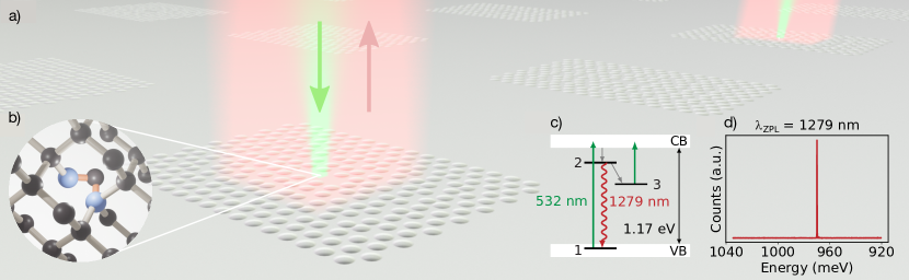
Our device, illustrated in Fig. 1a, consists of single G-centers coupled to inverse-designed 2D photonic crystal cavities. The G-center is a quantum emitter formed by two substitutional carbon atoms and a silicon interstitial (Fig. 1b), and features a zero phonon line (ZPL) transition at 970 meV (1279 nm) in the telecommunications O-band along with a spin triplet metastable state Udvarhelyi et al. (2021) (Figs. 1c, d).
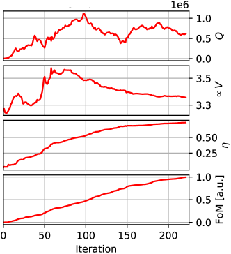
Our cavities were designed following our previous work Panuski et al. (2022) to simultaneously achieve a target while optimizing for vertical coupling by matching the emission to a narrow numerical aperture in the O-band. Fig. 2 shows one of our cavity designs, including its near-field cavity mode (Fig. 2a) and its far-field scattering profile (Fig. 2b), with more than 70% of the emitted power simulated to radiate into an objective NA of 0.55. More information on the optimization can be found in Methods, and the results of the cavity optimization in SI Section .3 and Fig. S1. The fabrication of our device follows our previous work Prabhu et al. (2022) with the addition of an underetch step, and is described in Methods.
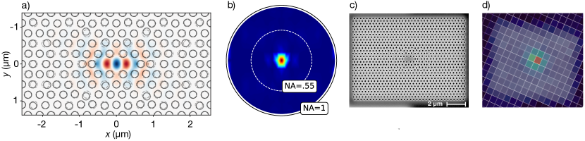
The measurements on our device were performed with a setup consisting of a home-built cryogenic confocal microscope featuring temperature and CO2 gas control, and optimized for visible light excitation and infrared collection into a single-mode fiber (details in SI Section .4). A scanning electron micrograph of a representative cavity in our chip is shown in Fig. 2c. Its reflectivity was characterized in cross-polarization Altug and Vucković (2005); Panuski et al. (2022); DeAbreu et al. (2022) (details in SI Section .5). Fig. 2d shows a photoluminescence (PL) 2D scan of one of our systems, where the cavity-coupled artificial atom is evidenced by the color-labeled IR emission in the cavity center upon excitation with green light. The spectral signature of the PL, shown in Fig. 1d, features a ZPL centered at around 1279 nm and thus aligns with the previously reported G-center ZPLs Hollenbach et al. (2020); Baron et al. (2021); Prabhu et al. (2022).
For the cavities of interest, we measure quality factors of and 2100, and center wavelengths around 1279 nm, near the G-center ZPL.
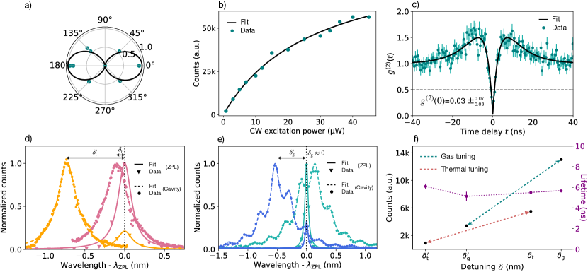
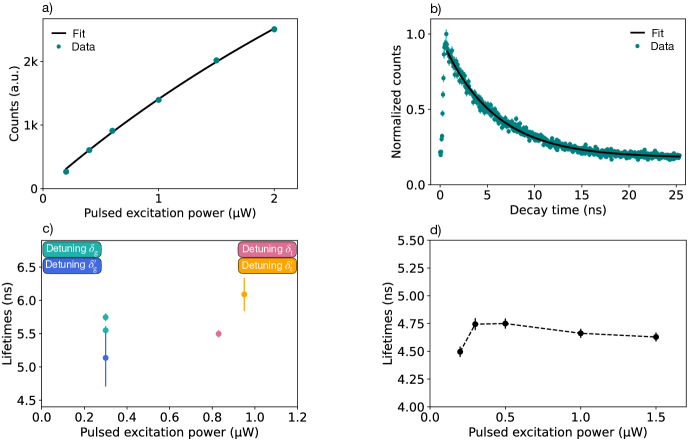
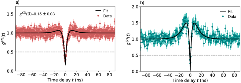
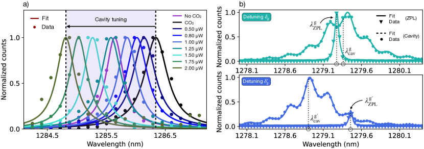
Fig. 3 shows the experimental results confirming the presence of single artificial atoms in our photonic crystal cavities. The coupling between the atom and the cavity results in an enhancement of the atom single-photon emission. We observe linearly polarized PL emission (Fig. 3a) from our system, indicative of coupling through the expected transverse electric cavity mode. Measuring the PL saturation under increasing excitation power yields that of a two-level emitter model (see Fig. 3b and SI Section .6). We further confirmed the addressing of a single artificial atom by demonstrating single-photon emission via a Hanbury-Brown-Twiss (HBT) experiment. Our second-order autocorrelation results (Fig. 3c) show excellent antibunching with a fitted value of without background correction (details in SI Section .7). This value is nearly an order of magnitude lower than the rest of the literature (see SI Table 1), and indicates high-purity single-photon emission. The bunching near ns delay conforms with the presence of a third dark state, which has been attributed to a metastable triplet state Udvarhelyi et al. (2021). These measurements demonstrate the presence of a single G-center in our cavity.
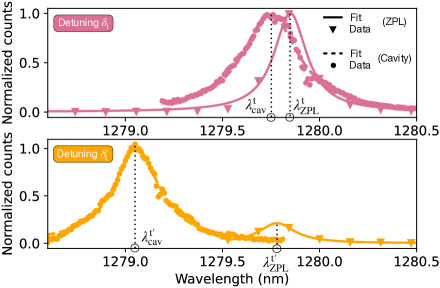
To confirm the cavity enhancement of our single artificial atom, we detuned the cavity resonance wavelength from the G-center ZPL using two different methods, i.e. thermal and gas tuning. In the thermal tuning experiments, starting with a cryostat temperature of 4 K, we brought the temperature up to 24 K and consequently shifted the cavity away from our G-center ZPL. This effect is visible in Fig. 3d, where the pink (orange) curves show the cavity and ZPL profiles before (after) the temperature increase. Different detunings and , defined as the difference between the cavity and ZPL wavelengths, are therefore achieved at 4 K and 24 K, respectively. While a significant cavity wavelength shift occurs, we also observe a much smaller ZPL shift, not shown in the figure. Therefore, this plot shall be indicative only of the relative shift between the cavity and ZPL wavelength. A more detailed discussion about the figure can be found in SI Section .8a. We note that temperatures below 30 K have been reported to not affect G-center ensembles Beaufils et al. (2018); Chartrand et al. (2018). We observe an intensity enhancement of with a cavity of and a mode volume of .
To validate that the intensity enhancement does not originate from the temperature change induced by thermal cavity tuning, we performed additional experiments using gas tuning. We injected CO2 gas into the cryogenic sample chamber to coat the cavity with solid CO2, followed by selective gas sublimation using a nm continuos wave (CW) laser. A further description of the process can be found in SI Section .8b. Analogously to the thermal tuning case, Fig. 3e shows the cavity reflectivity and G-center ZPL now under gas tuning for two different detunings and . We calculate an enhancement in the PL emission of with a cavity of and a mode volume of . Also in this case, we observe a ZPL shift (not shown in the figure). More details are to be found in SI Section .8b.
Ultimately, we measured the excited state lifetime of our artificial atoms under both gas and thermal tuning using a 0.5 ns pulsed laser at 532 nm for all cavity detunings (see SI Section .6 for details about these measurements). Fig. 3f shows our measured lifetimes and the emission rates for all of our experiments. We do not observe a statistically significant lifetime modification even under a clear cavity enhancement of the emission rates above 6x.
The quantum efficiency (QE) of any silicon color center is one of the central unanswered questions in the field. Recent reports have estimated the QE of a single G-center to be above 1% from waveguide-coupled counts Prabhu et al. (2022); Komza et al. (2022), and 10% for ensembles coupled to separate cavities Lefaucher et al. (2023). To gain a valid estimate of the QE of the G-center, an experiment varying the coupling rate between the same single artificial atom and a cavity was required. Our measurements allow us to extract such a value. Using the derivation described in SI Section .9 Lefaucher et al. (2023), the literature value of the Debye-Waller factor Beaufils et al. (2018), and our measured values of off-resonance lifetime ns and count rate enhancement for thermal tuning, we obtain a quantum efficiency bounded as .
III Discussion
We show, for the first time, strong enhancement of the quantum emission of individual artificial atoms coupled to silicon nanocavities. A central requirement for the scalability of our system is localized spatial and spectral alignment of both many cavities and many atoms to a common global frequency. The spatial alignment of the cavity and atom can be achieved by making use of the recently reported localized implantation of single G- and W-centers Hollenbach et al. (2022). Silicon artificial atoms can be spectrally aligned using the recently reported non-volatile optical tuning for G-centers Prabhu et al. (2022) or methods used in other artificial atom systems such as tuning via electric fields Anderson et al. (2019), or mechanical strain Wan et al. (2020). Cavity tuning via local thermal oxidation of silicon has been achieved on a large scale Panuski et al. (2022), and a similar method could be used to align large arrays of cavity-atom systems at room or cryogenic temperatures. Our approach directly applies to other silicon artificial atoms, such as the T-center, which would enable direct access to a spin outside of a metastable state Higginbottom et al. (2022).
A hypothesis was recently raised regarding the possibility of two different physical systems being reported as G-centers Baron et al. (2022). We believe that our work provides conclusive evidence for this claim. Table 1 in SI Section .10 compares the reported experimental results for single G-center labeled artificial atoms in silicon, and shows two clear clusters. The first group comprises the single emitter reports in Refs. Hollenbach et al. (2020); Baron et al. (2022); Prabhu et al. (2022); Komza et al. (2022), and aligns with G-center ensemble work Lefaucher et al. (2023). These studies show a ZPL centered around 1279 nm and a narrow inhomogeneous linewidth < 1.1 nm, a QE between 1 and 18%, and a short excited state lifetime < 10 ns that does not change significantly under Purcell enhancement, confirming the QE magnitude. The second group comprises Refs. Redjem et al. (2020, 2023), and features a shorter ZPL centered around 1270 nm and a larger inhomogeneous linewidth of 9.1 nm, a QE50%, and a longer excited state lifetime > 30 ns, which changes significantly under Purcell enhancement and thus qualitatively aligns with the estimated QE. Our measurements align with the first system, i.e. the originally reported G-centers, and provide the first upper bound for the QE of single G-centers, previously estimated to be between 1% Prabhu et al. (2022); Komza et al. (2022) and 10% for ensembles Lefaucher et al. (2023). More information on this comparison can be found in SI Section .10. We conclude that our work highlights the need for further theoretical and experimental investigation regarding the creation process and the photophysics of G-center-like artificial atoms in silicon platforms.
IV Conclusion
We showed cavity-enhanced single artificial atoms in silicon by integrating single G-centers into inverse-designed photonic crystal nanocavities. We demonstrated an intensity enhancement of 6x with a cavity featuring a , which yielded the highest purity single-photon emission for silicon color centers in the literature, and the first bound to the QE of single G-centers of %. Our demonstration lays the groundwork for efficient spin-photon interfaces at telecommunication wavelengths for large-scale quantum information processing in silicon.
Methods
IV.1 Sample fabrication
The fabrication process follows Redjem et al. (2020), starting from a commercial SOI wafer with nm silicon on µm silicon dioxide. Cleaved chips from this wafer were implanted with 12C with a dose of ions/cm2 and keV energy, and subsequently annealed at C for s to form G-centers in the silicon layer. The samples were then processed by a foundry (Applied Nanotools) for electron beam patterning and etching, resulting in through-etched silicon cavities with SiO2 bottom cladding and air as top cladding. The silicon etching was performed using inductively coupled plasma reactive ion etching with SF6-C4F8 mixed-gas. As a final step, the samples were under-etched in a solution of hydrofluoric acid for min and dried using a critical point dryer.
IV.2 Cavity far-field optimization
Traditional photonic crystal cavity optimization aims to cancel radiative loss to enhance quality factor , which also reduces collection efficiency. To avoid this, we incorporate the far-field collection efficiency to the optimization objective function alongside maximizing and minimizing mode volume Panuski et al. (2022) (Fig. S1). This process is implemented using the open-source package Legume Minkov et al. (2020) which maps the problem of cavity design onto efficient and auto-differentiable guided mode expansion (GME) for gradient-based optimization.
In practice, we observe quality factors much lower than the result expected from both simulation (Fig. S1) and previous statistical studies on thousands of photonic crystals designed for 1550 nm operation under the same optimization method Panuski et al. (2022). We attribute this disparity to the high carbon doping density used to produce cavity-coupled G-centers with sufficient probability. Reducing the doping density or applying localized doping Hollenbach et al. (2020) could play a role in recovering performance closer to intrinsic silicon. Applying large-scale characterization techniques Sutula et al. (2022) to locate ideal emitters and fabricate cavities around these positions could enhance the yield of coupled emitters in the case of reduced doping density.
Notes
Acknowledgements
The authors acknowledge Kevin C. Chen, Chao Li, Hugo Larocque and Mohamed ElKabbash for helpful discussions. C.E-H. and L.D. acknowledge funding from the European Union’s Horizon 2020 research and innovation program under the Marie Sklodowska-Curie grant agreements No.896401 and 840393. M.P. acknowledges funding from the National Science Foundation (NSF) Convergence Accelerator Program under grant No.OIA-2040695 and Harvard MURI under grant No.W911NF-15-1-0548. I.C. acknowledges funding from the National Defense Science and Engineering Graduate (NDSEG) Fellowship Program and NSF award DMR-1747426. M.C. acknowledges support from MIT Claude E. Shannon award. D.E. acknowledges support from the NSF RAISE TAQS program. This material is based on research sponsored by the Air Force Research Laboratory (AFRL), under agreement number FA8750-20-2-1007. The U.S. Government is authorized to reproduce and distribute reprints for Governmental purposes notwithstanding any copyright notation thereon. The views and conclusions contained herein are those of the authors and should not be interpreted as necessarily representing the official policies or endorsements, either expressed or implied, of the Air Force Research Laboratory (AFRL), or the U.S. Government.
References
- Bhaskar et al. (2020) M. K. Bhaskar, R. Riedinger, B. Machielse, D. S. Levonian, C. T. Nguyen, E. N. Knall, H. Park, D. Englund, M. Lončar, D. D. Sukachev, and M. D. Lukin, Nature 580, 60 (2020).
- Pompili et al. (2021) M. Pompili, S. L. N. Hermans, S. Baier, H. K. C. Beukers, P. C. Humphreys, R. N. Schouten, R. F. L. Vermeulen, M. J. Tiggelman, L. dos Santos Martins, B. Dirkse, S. Wehner, and R. Hanson, Science 372, 259 (2021).
- Childress and Hanson (2013) L. Childress and R. Hanson, MRS Bulletin 38, 134 (2013).
- Choi et al. (2019) H. Choi, M. Pant, S. Guha, and D. Englund, npj Quantum Information 5, 1 (2019).
- Degen et al. (2017) C. L. Degen, F. Reinhard, and P. Cappellaro, Reviews of Modern Physics 89, 035002 (2017).
- Redjem et al. (2020) W. Redjem, A. Durand, T. Herzig, A. Benali, S. Pezzagna, J. Meijer, A. Y. Kuznetsov, H. S. Nguyen, S. Cueff, J.-M. Gérard, I. Robert-Philip, B. Gil, D. Caliste, P. Pochet, M. Abbarchi, V. Jacques, A. Dréau, and G. Cassabois, Nature Electronics 3, 738 (2020).
- Higginbottom et al. (2022) D. B. Higginbottom, A. T. K. Kurkjian, C. Chartrand, M. Kazemi, N. A. Brunelle, E. R. MacQuarrie, J. R. Klein, N. R. Lee-Hone, J. Stacho, M. Ruether, C. Bowness, L. Bergeron, A. DeAbreu, S. R. Harrigan, J. Kanaganayagam, D. W. Marsden, T. S. Richards, L. A. Stott, S. Roorda, K. J. Morse, M. L. W. Thewalt, and S. Simmons, Nature 607, 266 (2022).
- Saeedi et al. (2013) K. Saeedi, S. Simmons, J. Z. Salvail, P. Dluhy, H. Riemann, N. V. Abrosimov, P. Becker, H.-J. Pohl, J. J. L. Morton, and M. L. W. Thewalt, Science 342, 830 (2013).
- Ruf et al. (2021) M. Ruf, N. H. Wan, H. Choi, D. Englund, and R. Hanson, Journal of Applied Physics 130, 070901 (2021).
- Zaporski et al. (2023) L. Zaporski, N. Shofer, J. H. Bodey, S. Manna, G. Gillard, M. H. Appel, C. Schimpf, S. F. Covre da Silva, J. Jarman, G. Delamare, G. Park, U. Haeusler, E. A. Chekhovich, A. Rastelli, D. A. Gangloff, M. Atatüre, and C. Le Gall, Nature Nanotechnology , 1 (2023).
- Purcell (1995) E. M. Purcell, in Confined Electrons and Photons: New Physics and Applications, NATO ASI Series, edited by E. Burstein and C. Weisbuch (Boston, MA, 1995) pp. 839–839.
- Bergeron et al. (2020) L. Bergeron, C. Chartrand, A. T. K. Kurkjian, K. J. Morse, H. Riemann, N. V. Abrosimov, P. Becker, H.-J. Pohl, M. L. W. Thewalt, and S. Simmons, PRX Quantum 1, 020301 (2020).
- Baron et al. (2021) Y. Baron, A. Durand, P. Udvarhelyi, T. Herzig, M. Khoury, S. Pezzagna, J. Meijer, I. Robert-Philip, M. Abbarchi, J.-M. Hartmann, V. Mazzocchi, J.-M. Gérard, A. Gali, V. Jacques, G. Cassabois, and A. Dréau, (2021), arXiv:2108.04283 [physics, physics:quant-ph] .
- Durand et al. (2021) A. Durand, Y. Baron, W. Redjem, T. Herzig, A. Benali, S. Pezzagna, J. Meijer, A. Y. Kuznetsov, J.-M. Gérard, I. Robert-Philip, M. Abbarchi, V. Jacques, G. Cassabois, and A. Dréau, Physical Review Letters 126, 083602 (2021).
- Hollenbach et al. (2020) M. Hollenbach, Y. Berencén, U. Kentsch, M. Helm, and G. V. Astakhov, Optics Express 28, 26111 (2020).
- DeAbreu et al. (2022) A. DeAbreu, C. Bowness, A. Alizadeh, C. Chartrand, N. A. Brunelle, E. R. MacQuarrie, N. R. Lee-Hone, M. Ruether, M. Kazemi, A. T. K. Kurkjian, S. Roorda, N. V. Abrosimov, H.-J. Pohl, M. L. W. Thewalt, D. B. Higginbottom, and S. Simmons, (2022), arXiv:arXiv.2209.14260 .
- Prabhu et al. (2022) M. Prabhu, C. Errando-Herranz, L. De Santis, I. Christen, C. Chen, and D. R. Englund, (2022), arXiv:2202.02342 [physics, physics:quant-ph] .
- Vivien and Pavesi (2016) L. Vivien and L. Pavesi, Handbook of Silicon Photonics (CRC Press, Boca Raton, FL, USA, 2016).
- Panuski et al. (2022) C. L. Panuski, I. R. Christen, M. Minkov, C. J. Brabec, S. Trajtenberg-Mills, A. D. Griffiths, J. J. D. McKendry, G. L. Leake, D. J. Coleman, C. Tran, J. S. Louis, J. Mucci, C. Horvath, J. N. Westwood-Bachman, S. F. Preble, M. D. Dawson, M. J. Strain, M. L. Fanto, and D. R. Englund, Nature Photonics 16, 834 (2022).
- Udvarhelyi et al. (2021) P. Udvarhelyi, B. Somogyi, G. Thiering, and A. Gali, Physical Review Letters 127, 196402 (2021).
- Altug and Vucković (2005) H. Altug and J. Vucković, Optics Letters 30, 982 (2005).
- Beaufils et al. (2018) C. Beaufils, W. Redjem, E. Rousseau, V. Jacques, A. Y. Kuznetsov, C. Raynaud, C. Voisin, A. Benali, T. Herzig, S. Pezzagna, J. Meijer, M. Abbarchi, and G. Cassabois, Physical Review B 97, 035303 (2018).
- Chartrand et al. (2018) C. Chartrand, L. Bergeron, K. J. Morse, H. Riemann, N. V. Abrosimov, P. Becker, H.-J. Pohl, S. Simmons, and M. L. W. Thewalt, Physical Review B 98, 195201 (2018).
- Komza et al. (2022) L. Komza, P. Samutpraphoot, M. Odeh, Y.-L. Tang, M. Mathew, J. Chang, H. Song, M.-K. Kim, Y. Xiong, G. Hautier, and A. Sipahigil, (2022), arXiv:2211.09305 [cond-mat, physics:physics, physics:quant-ph] .
- Lefaucher et al. (2023) B. Lefaucher, J.-B. Jager, V. Calvo, A. Durand, Y. Baron, F. Cache, V. Jacques, I. Robert-Philip, G. Cassabois, T. Herzig, J. Meijer, S. Pezzagna, M. Khoury, M. Abbarchi, A. Dréau, and J.-M. Gérard, Applied Physics Letters 122, 061109 (2023).
- Hollenbach et al. (2022) M. Hollenbach, N. Klingner, N. S. Jagtap, L. Bischoff, C. Fowley, U. Kentsch, G. Hlawacek, A. Erbe, N. V. Abrosimov, M. Helm, Y. Berencén, and G. V. Astakhov, Nature Communications 13, 7683 (2022).
- Anderson et al. (2019) C. P. Anderson, A. Bourassa, K. C. Miao, G. Wolfowicz, P. J. Mintun, A. L. Crook, H. Abe, J. Ul Hassan, N. T. Son, T. Ohshima, and D. D. Awschalom, Science 366, 1225 (2019).
- Wan et al. (2020) N. H. Wan, T.-J. Lu, K. C. Chen, M. P. Walsh, M. E. Trusheim, L. De Santis, E. A. Bersin, I. B. Harris, S. L. Mouradian, I. R. Christen, E. S. Bielejec, and D. Englund, Nature 583, 226 (2020).
- Baron et al. (2022) Y. Baron, A. Durand, T. Herzig, M. Khoury, S. Pezzagna, J. Meijer, I. Robert-Philip, M. Abbarchi, J.-M. Hartmann, S. Reboh, J.-M. Gérard, V. Jacques, G. Cassabois, and A. Dréau, Applied Physics Letters 121, 084003 (2022).
- Redjem et al. (2023) W. Redjem, Y. Zhiyenbayev, W. Qarony, V. Ivanov, C. Papapanos, W. Liu, K. Jhuria, Z. A. Balushi, S. Dhuey, A. Schwartzberg, L. Tan, T. Schenkel, and B. Kanté, (2023), arXiv:2301.06654 [quant-ph] .
- Minkov et al. (2020) M. Minkov, I. A. D. Williamson, L. C. Andreani, D. Gerace, B. Lou, A. Y. Song, T. W. Hughes, and S. Fan, ACS Photonics 7, 1729 (2020).
- Sutula et al. (2022) M. Sutula, I. Christen, E. Bersin, M. P. Walsh, K. C. Chen, J. Mallek, A. Melville, M. Titze, E. S. Bielejec, S. Hamilton, D. Braje, P. B. Dixon, and D. R. Englund, (2022), arXiv:2210.13643 .
- Gritsch et al. (2023) A. Gritsch, A. Ulanowski, and A. Reiserer, (2023), arXiv:2301.07753 [quant-ph] .
- Lin et al. (2021) Z. Lin, L. Schweickert, S. Gyger, K. D. Jöns, and V. Zwiller, Journal of Instrumentation 16, T08016 (2021).
- Warren (1986) S. G. Warren, Applied Optics 25, 2650 (1986).
- Ismail et al. (2016) N. Ismail, C. C. Kores, D. Geskus, and M. Pollnau, Optics Express 24, 16366 (2016).
Supplementary Information
.3 Cavity optimization
Figure S1 shows the course of optimization for the two cavities we employed in our experiments, with the only difference being the hole sizes. Sweeps with several varying parameters (e.g. lattice constant, cavity and hole size) were fabricated in order to target systems with the desired performance.
.4 Measurement setup
Fig. S2 shows a schematic of our measurement setup, which consists of 3 main optical paths: 1) excitation, 2) cryogenic 4F, and 3) collection.
The excitation path combines IR and visible collimated lasers with a dichroic, and routes them via a linear polarizer into a polarizing beam splitter (PBS). For our characterization, we use two visible lasers and two infrared lasers. Our visible lasers consist of a continuous wave Coherent Verdi G5 at 532 nm, and a pulsed laser from NKT Photonics SuperK laser with a maximum repetition rate of 78 MHz and filtered by a bandpass filter centered at 532 nm with a bandwidth of 0.2 nm. Our infrared lasers are a tunable CW O-band TSL570C from Santec, and a superluminescent diode S5FC1018S from Thorlabs with a broadband emission centered at 1310 nm. A set of scanning mirrors is placed in the excitation path for precise beam positioning and PL mapping of our cavities.
The transmitted polarization component is imaged into our cryostat by using a 4F lens system consisting of scanning piezoelectric mirrors, two lenses, and an objective, with preceding IR quarter and half wave plates for polarization rotation. Our microscope objective is a collar corrected objective LCPLN50XIR from Olympus with a NA of 0.65, and is external to the cryostat. Our cryostat is a Montana Instruments system. The sample is mounted on a XYZ cryogenic piezoelectric stage (Attocube).
The PL and reflection from our sample are collected via the PBS reflection through an IR polarizer and a filtering station into a fiber switch, which routes the collected light into superconducting nanowire single-photon detectors (SNSPDs) or an IR spectrometer. Our filtering setup consists of a longpass filter (cutoff wavelength at 1250 nm) and a shortpass filter (cutoff wavelength at 1300 nm). Additionally, in several experiments we used a tunable fiber filter from WLPhotonics with FWHM transmission bandwidth of nm. Our two SNSPDs (NIST) feature detection efficiencies of and , and are readout with a Swabian Instruments Timetagger 20. Our IR spectrometer consists of a PyLon IR CCD from Princeton Instruments and switchable gratings, one with a density of 300 gr/mm and a 1.2 µm blaze and another with a density of 900 gr/mm and a 1.3 µm blaze, leading to pixel-defined resolutions of 155 pm and 40 pm respectively. For the second-order autocorrelation measurements we used a fiber beam splitter (Thorlabs TW1300R5F1) after the filtering station. In addition, we image our sample using a flip mirror before the fiber switch and an InGaAs cooled CCD camera (Allied Vision Goldeye), preceded by a flip lens that allows us to switch between near-field and far-field imaging.
The setup comprises also a gas line equipped with a needle valve and several ball valves to enable controllable gas injection into our cryostat.
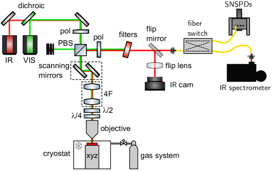
.5 Cross-polarization cavity characterization
We characterized our cavities via a cross-polarization measurement, as previously reported in Ref. Altug and Vucković (2005). The measurement protocol consists of preparing the polarization of the input and output IR beams to be orthogonal and rotated with respect to the cavity axis. This was achieved by setting the input and output polarizers perpendicular to each other, and by rotating the common half-wave plate to align the fields to the cavity (see schematic in Fig. S2). In our setup, we used a PBS for increased polarization extinction.
.6 Measurements under pulsed excitation
All measurements under pulsed excitation were performed with our SuperK laser using a repetition rate of 39 MHz, and varying the power from a minimum of 0.2 W to a maximum of 2 W.
As already discussed in the main text, our artificial atom emission fits well to the characteristic two-level emitter saturation model, which is given by
| (3) |
Here, and are intensity and power, respectively, and and are the corresponding saturation values. Fitting our experimental data to this theoretical model, we find ) kcounts/min and W. The data and corresponding fit are shown in Fig. S3a. The same theoretical model is used to fit the data taken under CW excitation power reported in the main text. In that case (Fig. 3b in the main text), we obtain ) kcounts/min and W.
Fig. S3b shows an example of our lifetime data and fits. The plot displays one data set acquired at detuning (refer to Fig. 3e in the main text) with a pulsed excitation power of 0.3 W fitted to a mono-exponential model
| (4) |
with being a fitting constant for the amplitude, and and offsets for the decay time and , respectively. The fit returns a lifetime of ns. All lifetime data sets are fitted using the same model, which returns the lifetime values plotted in Fig. S3c for all the detuning values. In both thermal and gas tuning cases, the lifetime does not differ significantly for different detunings. This figure displays the values that are used to estimate the bound on the QE. The single value shown in Fig. 3f in the main text for detuning is the weighted average between the two values reported in Fig. S3c. However, for the sake of completeness, we also report additional lifetimes acquired at detuning under likely different laser conditions, originating from an error related to our laser control electronics board. The values are shown in Fig. S3d. In this case, we measure lifetimes all below ns. As these measurements were taken under possibly different experimental conditions, we decided not to include them in our theoretical analysis. However, they confirm that the lifetime of our emitter remains essentially unchanged with increasing excitation power.
.7 Second-order autocorrelation measurements
The second-order autocorrelation measurements were performed using a HBT interferometer. We excited each of our emitters with a nm CW pump and sent the generated photons to a fiber beam splitter whose outputs were connected to two SNSPDs, and we then analyzed the coincidence counts at different time delays between the two outputs. Fitting our second-order autocorrelation data with a three-level system equation
| (5) |
with , , and fitting parameters, the offset for the time delay , and and the lifetimes, we obtain the value after data normalization as at . HBT measurement data and fits are shown in Figs. S4a and b for the thermal tuning and gas tuning cases, respectively. In both cases we obtain a close to 0, thus confirming genuine single-photon emission. In the gas tuning case, we find , ns and ns. The data was collected filtering the region around the ZPL, and thus reducing the noise contribution coming from elsewhere. In the thermal tuning case, we used the longpass and shortpass filters to isolate a nm-wide region comprising the ZPL, while we improved the gas-tuning measurement by filtering a much narrower region with the only help of the electrically tunable bandpass fiber filter described in SI Section .4. We used a CW excitation power of 6 W (10 W) in the thermal (gas) tuning case. In both cases the data was acquired as raw time tags and is not background-corrected. The coincidence counts were evaluated with the software ETA Lin et al. (2021) using a time binning of ps ( ps) in the thermal (gas) tuning case.
The G-center is known to feature three energy levels: a ground and excited singlet state and a metastable triplet state Udvarhelyi et al. (2021). The metastable state introduces a bunching effect in the second-order correlation, and has been previously observed for G-centers Redjem et al. (2020); Hollenbach et al. (2020). This bunching effect is clearly visible in Fig. S4b, while it is less evident in Fig. S4a. We attribute this difference to the fact that different emitters have different electron trapping rates and other mesoscopic properties that dictate the bunching.
.8 Tuning of cavity resonances
Here we expand on the methods used to decouple the G-centers from our cavities. As mentioned in the main text, we performed both thermal and gas tuning to achieve decoupling.
.8.1 Thermal tuning
Starting with a cryostat chamber temperature of K, we define the detuning as , where is the G-center ZPL wavelength and the cavity resonance wavelength. Fitting both the cavity and ZPL profiles to a Lorentzian function, we find the wavelengths to be nm and nm, and thus calculate nm. The cavity and ZPL profiles at K are displayed in pink in Fig. S5. The extracted factor of our cavity is .
In order to decouple the cavity-atom system, we warmed up the chamber to K and observed the subsequent effect. As visible in orange in Fig. S5, the cavity shifted away spectrally from the ZPL, resulting in a reduction of the ZPL intensity. The cavity resonance is now found at nm, and a less significant spectral shift is also observed in the ZPL wavelength, now at nm. The latter effect is in line with what we recently reported in Ref. Prabhu et al. (2022), where a non-volatile spectral shift in the ZPL of our single G-centers was observed. After the temperature variation, the detuning is found to be nm. Fig. 3d in the main text condenses this information by combining both detuning cases and in one plot. To highlight these detunings between the cavity and ZPL, we shifted the x-axis of the bottom plot in Fig. S5 by ( - ). In this way, the detunings between the cavity and ZPL are more clearly visible. However, because of this shift, it should be noted that the plot in Fig. 3d does not reflect the real difference between the cavity wavelengths before and after tuning. This information is preserved in Fig. S5.
All spectra were acquired with a grating density of gr/mm. The cavity reflectivity measurements were performed with our tunable CW narrowband IR laser while sweeping its wavelength and recording the cavity spectrum at each step. All spectra were then merged to obtain the complete cavity profile.
.8.2 Gas tuning
To validate what we observed in the thermal tuning case, we spectrally shifted the cavity of a second cavity-atom system via a different tuning mechanism based on gas deposition and subsequent sublimation. In this case, the chamber temperature remained constant (at K) throughout our measurements. First, we coated our sample with a thin layer of gas (CO2) by injecting the gas into our cryostat chamber via a dedicated gas line. The gas layer alters the mode index of the cavity and thus redshifts its wavelength. We assume first-order perturbation theory and follow the derivation in the SI of Ref. Panuski et al. (2022). Using a refractive index for solid CO2 of 1.4 Warren (1986), and a representative mode for the photonic crystal cavity, we estimate a resonance shift of the order of nm for an infinite thickness of solid CO2.
We then performed gradual gas sublimation to achieve a controllable cavity resonance blueshift. Fig. S6a shows a representative experimental gas shifting of cavity spectra. Our maximum tuning, in the order of nm, aligns reasonably well with our theoretical estimate. Starting from the nominal cavity resonance wavelength (purple curve), we injected CO2 and thus redshifted the cavity mode (black curve). We then illuminated the cavity with a nm CW pump for s at increasingly higher powers (displayed in the figure’s legend), and thus achieved a controllable cavity resonance shift. We note that our cavity blueshifts further than its initial central wavelength, indicating that there is likely a significant leakage of CO2 or other gases during the cooling, which we can sublimate using our optical pumping technique.
After depositing CO2 on our sample, we acquired the ZPL and cavity spectra. We find their center wavelengths to be nm and nm, leading to a very small detuning of nm as shown in green in Fig. S6b. Unlike the previous case, the cavity reflectivity measurements shown in Fig. S6b were performed with our superluminescent diode by simply illuminating the cavity and recording its reflectivity spectrum. Moreover, these spectra were acquired with a higher resolution compared to the previous experiments (here we used a grating density of gr/mm) which resulted in a slight wavelength offset likely due to calibration errors. This offset was taken into account when plotting the data, in order to enable a fair wavelength comparison between the thermal and gas tuning cases.
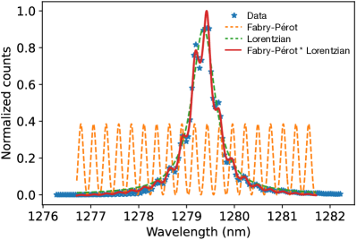
While the value of was still obtained by fitting the ZPL profile to a Lorentzian function, the cavity spectrum required a different analysis due to the presence of parasitic oscillations in its profile, as visible in Fig. S6b. This behaviour was not observed in the thermal tuning case because of the lower resolution arising from a smaller grating density. It is known that these parasitic cavities are Fabry-Pérot (FP) cavities arising from reflections in the silicon substrate Panuski et al. (2022). A FP cavity is described by an airy distribution Ismail et al. (2016) as
| (6) |
with an amplitude fitting constant, , the optical frequency detuning, the cavity free spectral range with the speed of light and the cavity length, and and the mirror reflectivities.
The photonic crystal cavity resonance is described by a Lorentzian as follows
| (7) |
with and being fitting constants for the amplitude and offset, and the wavelength and wavelength offset, and the full width at half maximum (FWHM). We estimate the effect of the coupled system by using a product function
| (8) |
We extract a cavity Q factor of .
To decouple our cavity-atom system, we illuminated a region in the vicinity of our cavity with nm CW laser light with powers up to 500 W. This resulted in a shift of our cavity resonance wavelength from to nm. We note that also in this case the optical pumping required for gas tuning introduces a non-volatile spectral shift in the ZPL of our single emitters, as reported in Ref. Prabhu et al. (2022). The ZPL wavelength reads now nm. A detuning of nm is therefore achieved. These results are shown in blue in Fig. S6b. Considerations analogous to how the plot in Fig. 3d is realized (see previous subsection) hold for Fig. 3e as well.
.9 Derivation of quantum efficiency
In the following, we derive the relevant rates from first principles and use them to estimate the G-center quantum efficiency of our system. We assume that 1) the cavity detuning does not significantly affect the Purcell factor of non-ZPL radiative phenomena (part of ), and that 2) there is a negligible contribution of other radiative modes in our measurements due to our nm narrow filtering of the ZPL. Under these assumptions, we write the total emission rate and the collected photon flux for both the on- and off-resonance cases as
| (9) | ||||
| (10) | ||||
| (11) | ||||
| (12) |
with the Purcell factor and the coupling efficiency into the wanted mode extracted from our simulations in Fig. 2. The quantum efficiency QE is defined as
| (13) |
where is the Debye-Waller factor, i.e. the fraction of the PL intensity emitted in the ZPL, and is extracted from the literature. Extracting from the equation above and substituting it in the ratio between Eqs. 9 and 10, that is , we find an expression for as a function of QE:
| (14) |
Following the procedure in Ref. Lefaucher et al. (2023), given that in our measurements the lifetimes remain constant within the error, we can define a bound on our QE by setting a threshold for the detection of the longest lifetime allowed by our off-resonance standard deviation . As the on- and off-resonance lifetimes do not differ significantly, it holds that . Therefore, we can derive an upper bound for the QE:
| (15) |
.10 Comparison to the G-center literature
Table 1 summarizes the reported literature on single emitters in silicon identified as G-centers in terms of their ZPL, estimated QE, , and excited state lifetimes. We include a recent report on cavity-coupled ensembles Lefaucher et al. (2023) and the simultaneous report on cavity-enhancement of singles Redjem et al. (2023), and use these to add cavity-enhanced excited state lifetime and to the comparison. What reported in Table 1 aligns with the hypothesis, originally brought forward by Ref. Baron et al. (2022), that the community is likely studying two different defects. The first one, which we label Hollenbach et al. (2020); Baron et al. (2022); Hollenbach et al. (2022); Prabhu et al. (2022); Komza et al. (2022); Lefaucher et al. (2023), aligns with the original G-center ensembles, and features a ZPL at around nm with a narrow inhomogeneous linewidth, a lower QE, and a short excited state lifetime. The second one, Redjem et al. (2020, 2023), features a blue-shifted ZPL at nm with a high QE and a longer excited-state lifetime.
Although our results suggest the possibility of two different artificial atom systems, the reported differences may still be due to a different host material, measurement setups, or fabrication protocols.
| Reference | ZPL | QE | Notes | ||||
|---|---|---|---|---|---|---|---|
| (nm) | () | (ns) | (ns) | ||||
| Redjem et al. Redjem et al. (2020) | * | 0.3 | 29 emitters | ||||
| Hollenbach et al. Hollenbach et al. (2020) | 12 µm SOI, 12 emitters | ||||||
| Baron et al. Baron et al. (2022) | 1 emitter measured | ||||||
| Hollenbach et al. Hollenbach et al. (2022) | 1 emitter measured | ||||||
| Prabhu et al. Prabhu et al. (2022) | >1* | Waveguide, 37 emitters | |||||
| Komza et al. Komza et al. (2022) | >2* | Waveguide, 1 emitter | |||||
| Redjem et al. Redjem et al. (2023) | 4862 | L3 cavity, 1 emitter | |||||
| Lefaucher et al. Lefaucher et al. (2023) | <10** | 417 | Ensembles, static rings | ||||
| This work | <18 | Opt. L3 cavity, 1 emitter |
*