Authors to whom correspondence should be addressed: ] ssyeh@nycu.edu.tw (S.S.Y.) and jjlin@nycu.edu.tw (J.J.L.)
Authors to whom correspondence should be addressed: ] ssyeh@nycu.edu.tw (S.S.Y.) and jjlin@nycu.edu.tw (J.J.L.)
Quantum-interference origin and magnitude of 1/ noise in Dirac nodal line IrO2 nanowires at low temperatures
Abstract
We present 1/ noise measurements of IrO2 nanowires from 1.7 to 350 K. Results reveal that the noise magnitude (represented by Hooge parameter ) increases at low temperatures, indicating low-frequency resistance noise from universal conductance fluctuations. The cause of this noise is determined to be due to oxygen vacancies in the rutile structure of IrO2. Additionally, the number density of these mobile defects can be calculated from the resistance rise caused by the orbital two-channel Kondo effect in the Dirac nodal line metal IrO2.
The metal iridium dioxide (IrO2) has drawn significant attention as a promising material for spintronic applications due to its giant spin Hall resistivity.Fujiwara et al. (2013) IrO2 is also widely used in glucose and pH sensors.Dong et al. (2018) Recently, the elusive orbital two-channel Kondo (2CK) effect was observed in IrO2 nanowires (NWs).Yeh et al. (2020) It results in a square-root-in-temperature increase of the resistivity, i.e., (where is resistivity, and is temperature) below a characteristic temperature due to oxygen vacancies (VO’s).Yeh et al. (2020) These observations make IrO2 NWs an attractive platform for exploring strongly correlated electron systems.Kirchner (2020) Despite its potential, there is limited information on the low- low-frequency noise and its origin in IrO2. The noise is a key factor which will ultimately limit the performance of every nanoelectronic device.Balandin (2013)
The standard theory of 1/ noise in metals assumes the existence of mobile defects, often modeled as a set of independent two-level systems (TLSs) with a wide distribution of relaxation times. It can be shown that the resulting resistance fluctuations power spectrum density (PSD) possesses a dependence, with .Dutta and Horn (1981); Weissman (1988); Fleetwood (2015) In this study, we examine the relationship between the number density of mobile defects () in IrO2 NWs and the noise measured within the range of 1.7 to 350 K. We find unexpected results at low , where the noise magnitude increases with decreasing . We explain that this low- noise originates from the universal conductance fluctuations (UCF), which stem from quantum interference of conduction electrons scattered off mobile defects.Giordano (1991); Feng (1991); Gupta (1994) We identify these mobile defects are associate with the VO’s in the IrO2 rutile structure. While 1/ noise has been measured in a wide variety of conductors, both the origin and the amount of the underlying mobile defects in a given material are usually difficult to identify and quantize. In the present case, we demonstrate that combined with the measurements of the 2CK effect, the value in every NW can be inferred.
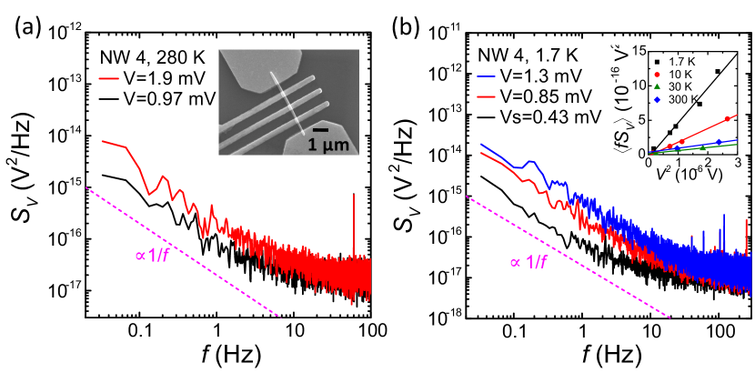
Our IrO2 NWs were grown via the metal-organic chemical vapor deposition method.Chen et al. (2004a); Lin et al. (2008) The single-crystalline rutile structure was characterized by selected-area electron diffraction patternsChen et al. (2004a) and X-ray diffraction (XRD) patterns.Chen et al. (2004b) To generate VO’s, the NWs were thermally annealed at 300∘C in vacuum. The annealing time was 3 h for NWs 1 to 3, and 4 h for NW 4. To facilitate electrical measurements, submicron Cr/Au (10/120 nm) electrodes attaching a NW device were fabricated by the electron-beam lithographic technique. The inset of Fig. 1 shows a scanning electron microscopy (SEM) image of a typical NW device. An ac method for 1/ noise measurement was applied.Scofield (1987) The background voltage noise PSD in our setup was V2/Hz, which was limited by the voltage preamplifier (Stanford Research model SR560). The relevant parameters of the four IrO2 NWs studied in the present work are listed in Table 1.
| Nanowire | (m) | (nm) | (m-3) | ||
|---|---|---|---|---|---|
| NW 1 | 1.9 | 143 | 0.074 | 0.0015 | |
| NW 2 | 1.0 | 123 | 0.020 | 0.0019 | |
| NW 3 | 0.75 | 125 | 0.037 | 0.0018 | |
| NW 4 | 0.90 | 147 | 0.065 | 0.0010 |
Power spectrum density and Hooge parameter . For an ohmic conductor under a small bias current , the measured voltage noise is usually expressed by the empirical formHooge (1969)
| (1) |
where is the Hooge parameter which characterizes the 1/ noise magnitude, is the total carrier number in the sample, is the voltage dropped on the sample.
Figures 1(a) and (b) show the measured of NW 4 at two representative temperatures 280 and 1.7 K, respectively. Above several tens Hz, the measured approaches a constant (). At lower frequencies, increases with decreasing , as well as with increasing . A dependence, with , is found for Hz. This dependence can be well described by Eq. (1). To extract the value, we rewrite Eq. (1) as , where denotes the average of the product of each discrete and in the data set in the regime. The inset of Fig. 1(b) shows that our data obey the dependence at our measurement temperatures. Thus, the value can be obtained from a linear fit of the slope , where , with m-3 being the carrier density of IrO2,Kawasaki et al. (2018) () the length (diameter) of the NW. The linear dependence suggests that the measured voltage noise originates from the resistance fluctuations in the NW, i.e., the (small) applied only acts as a sensitive electrical probe, while it does not drive the resistance fluctuations.Hooge (1969)
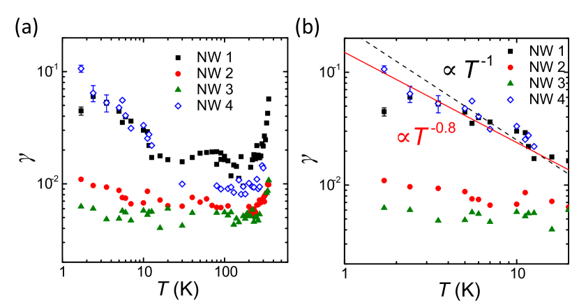
The extracted values as a function of between 1.7 and 350 K for four IrO2 NWs are plotted in Fig. 2(a). As decreases from 350 K, first decreases and then saturates below around 100 K. For example, the value of NW 4 decreases from 0.014 at 300 K to 0.009 at 100 K, and then remains constant until about 20 K. In this high- regime, we expect that the TLSs are thermally activated and the noise essentially follows the local-interference model.Pelz and Clarke (1987) In the rest of this Letter, we shall focus our discussion on the noise below 20 K, which results from the UCF in the NWs.
UCF-induced 1/ noise. The most interesting observation of this work is that, below about 20 K, our extracted values increase with decreasing in all NWs. This extraordinary behavior is particularly significant in NWs 1 and 4. In NW 4, the value of at 1.7 K is [] and is one order of magnitude larger than that at 30 K, and even larger than that at 300 K. Figure 2(b) shows that NW 1 has behavior similar to that of NW 4, except that the value saturates below 3 K. The low- increase of in NWs 2 and 3 is smaller than that in NWs 1 and 4.
The rapid and repeated switching of mobile defects or TLSs modifies (a large fraction of) the electron paths traversing the NW. The resulting quantum interference among the electron trajectories is sensitively altered. The interference effect becomes more pronounced at lower , where the electron dephasing time () well surpasses the electron elastic mean free time (), i.e., . This is the origin of the temporal UCF.Feng (1991); Giordano (1991) In 1991, Feng realized that UCF in turn could give rise to 1/ noise. He showed that the phenomenological Hooge parameter was directly connected with the variance of the conductance fluctuations, and given by,Feng (1991); Giordano (1991)
| (2) |
where () denotes the maximum (minimum) frequency of the mobile defects which are relevant in the measurement, is the conductance of the sample, and is the variance of the UCF. Because increases as the quantum-interference effect increases, grows with decreasing . An additional -dependence of may be due to the saturation of (i.e., becomes nearly independent of ) as .Lin and Bird (2002)
As the electron dephasing length , , where is the electron diffusion constant and is the Fermi velocity, our NWs are essentially three-dimensional (3D). We consider the UCF in the “saturated” regime, which is defined by , where is the number density of total (static and mobile) defects, is the electron elastic mean free path, and is the averaged electron scattering cross section. This is the regime that is pertinent to our NWs, see Table 1. The UCF theory predicts under these conditions the normalized varianceFeng (1991)
| (3) |
where is the Fermi wavenumber. Thus, the dependence is fully determined by the behavior of . In writing down Eq. (3), the thermal energy averaging effect has been ignored which presumably would introduce another characteristic length scale, the thermal diffusion length , into the cutoff of the UCF ( is the Planck constant divided by 2, and is the Boltzmann constant). We have previously found that the thermal energy averaging effect on the UCF magnitude was negligibly smaller than theoretically predicted.Yang et al. (2012) Thus, we take Eq. (3) to be sufficient for providing a good understanding of the data.
Figure 2(b) shows that below about 20 K, in NW 4. This dependence can be readily explained in terms of an electron dephasing rate , where the first term has been widely observed in experiments and is called the saturated electron dephasing rate as .Lin and Bird (2002) The second term is the electron-phonon scattering rate which dominates the inelastic scattering in weakly disordered metals.Zhong et al. (2010); Zhong and Lin (1998) In NW 1, shows a similar behavior until it saturates below about 3 K, indicating that is much larger in this NW than in NW 4.Trionfi, Lee, and Natelson (2007) The magnitudes of increase in NWs 2 and 3 are small, because these two NWs have comparatively small values (see below).
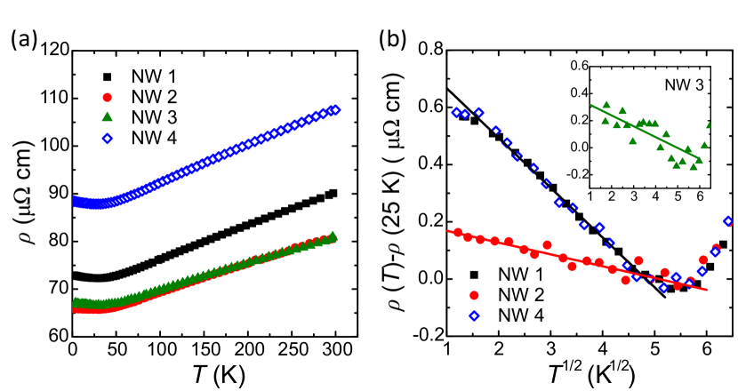
Identifying the origin and number density of mobile defects. We will now delve into the examination of the microscopic source of mobile defects responsible for inducing UCF and determining the 1/ noise magnitude in IrO2 NWs, including their number density. This is based on nonmagnetic orbital 2CK physics which was recently reported in this material. The 2CK effect in IrO2 causes a increase of at low . Figure 3(a) shows the variation of with for our NWs. reveals typical Boltzmann transport behavior until below about 25 K where it slightly increases with decreasing . Close inspection indicates that this increase obeys a dependence down to 2 K, Fig. 3(b). Between 2 and 25 K, the normalized increase is in our NWs. This amount of resistivity increase is more than one order of magnitude larger than what would be expected from the 3D weak localization and electron-electron interaction effects.Lee and Ramakrishnan (1985); Yeh et al. (2020) We have recently demonstrated that this increase obeys Affleck and Ludwig (1993)
| (4) |
where denotes the number density of 2CK scatterers, is the density of states at the Fermi energy per spin per channel, and is a characteristic temperature scale in the 2CK problem.
Oxygen vacancies frequently occur in IrO2 which assumes the rutile structure, depending on the sample preparation conditions.Yeh et al. (2020) Due to charge neutrality, a VO generates two “defect electrons” in IrO2. One of the two defect electrons, which occupies the doubly degenerate 5 or 5 iridium ion orbital, is strongly coupled to the two equivalent and independent spin-up and spin-down conduction-electron channels. This is the origin of the 2CK effect in IrO2.Yeh et al. (2020); Kirchner (2020) With the assumption that the density of VO’s, denoted by , is low enough to safely ignore any correlations between VO’s, we can estimate in each IrO2 NW.
To compare our data with Eq. (4), we take K, the temperature below which the behavior is found. Then, the value in each NW can be extracted from the fitted slope plotted in Fig. 3(b), using J-1 m-3 and m/s for IrO2.Lin et al. (1999); Yeh et al. (2020) These values are listed in Table 1. We see that NWs 1 and 4, which have the largest noise magnitudes , also show the largest resistivity increases (i.e., largest values), and NWs 2 and 3 have smaller noise magnitudes and simultaneously smaller resistivity increases (i.e., smaller values).
In practice, the mobile defects existing in a given sample may not all contribute to a given noise measurement, and will be given by the number of those defects having switching frequency . Then, . In the regime where the resistance fluctuations are governed by the local-interference (LI) mechanism and holds, we obtain an estimate for the switching TLS density . This is accomplished by applying a method developed earlier,Yeh et al. (2018) where can be estimated with the measured value through , where () is the electronic charge (effective mass). At 30 K, this gives in the present case m-3 for NWs 1 and 4, and m-3 for NWs 2 and 3. These extracted values scale with and are smaller than the values within a factor of 10, indicating the fluctuators at low are associated with the VO’s. Thus, in our NWs, we estimate has values m-3, being about one order of magnitude larger than that found in, e.g., Bi films.Birge, Golding, and Haemmerle (1989)
One possible explanation for this is the existence of an interstitial oxygen density that is (by and large) proportional to . Our thermal annealing studies suggest that this is not the reason for the proportionality between and , as an increase in annealing time in vacuum is expected to reduce the number density of oxygen interstituals while increasing . This leaves us with the more interesting alternative that the VO’s themselves are driving the 1/ noise.
The characteristic feature of the one-channel (two-channel) Kondo effect is the existence of a degenerate local level hybridizing with a band (two bands) of electron states. This leads to a characteristic energy scale known as the Kondo temperature () or equivalently a characteristic time scale .Hewson (1993) (In the present case, = .) On the other hand, 1/ noise is associated with a broad distribution of relaxation times of the mobile defects. To ensure that the 2CK effect can form in IrO2, the degeneracy between 5 and 5 has to remain intact even in the presence of such a broad distribution. Moreover, to guarantee that the flickering is not interfering with the formation of the 2CK effect, needs to hold. This is evidently satisfied, as can be inferred from Fig. 1 with K as is appropriate for IrO2 NWs. The necessary broad distribution of relaxation times of the fluctuators driving the 1/ noise implies a corresponding disorder distribution of the VO environment. That the value distribution in such a situation remains sharply peaked has been addressed before.Chakravarty and Nayak (2000) A microscopic model of how VO’s can drive an orbital Kondo effect and concomitantly 1/ noise at lower frequencies is left for future work. Intuitively, if different VO’s reside at varying distances to grain boundaries, and grain boundaries in the NW have differing orientations, a distribution of the relaxation times should naturally arise. NW surfaces (and the interface with substrate) could likely have similar effects on resulting in a distribution of relaxation times. In any case, our recent experiments have confirmed that the 1/ noise magnitude in a series of RuO2 films is controlled by , which can be reversely adjusted, i.e., increased or reduced, by annealing RuO2 in vacuum, air, or oxygen gas.Yeh et al. (2018) Since both RuO2 and IrO2 crystallize in the rutile structure and have similar physical propertiesLin et al. (2004) (except that RuO2 is antiferromagnetic which leads to an orbital one-channel Kondo effect at low , see Ref. Yeh et al., 2020), we expect that VO’s play a similar role in producing 1/ noise in IrO2.
Temporal resistance fluctuations. While the UCF-induced 1/ noise has been theoretically proposed in the 1980s,Feng, Lee, and Stone (1986) the predictions have not been widely tested. The reasons are that one needs to use microscale samples and measure the noise down to low . Otherwise, the quantum-interference effect will be negligible and the noise magnitude small and difficult to detect. To further check that the measured 1/ noise in IrO2 below 20 K is caused by the UCF mechanism, we have extracted the (normalized) variance of conductance fluctuations from an independent measurement, and compare it with that calculated from the measured value through Eq. (2).
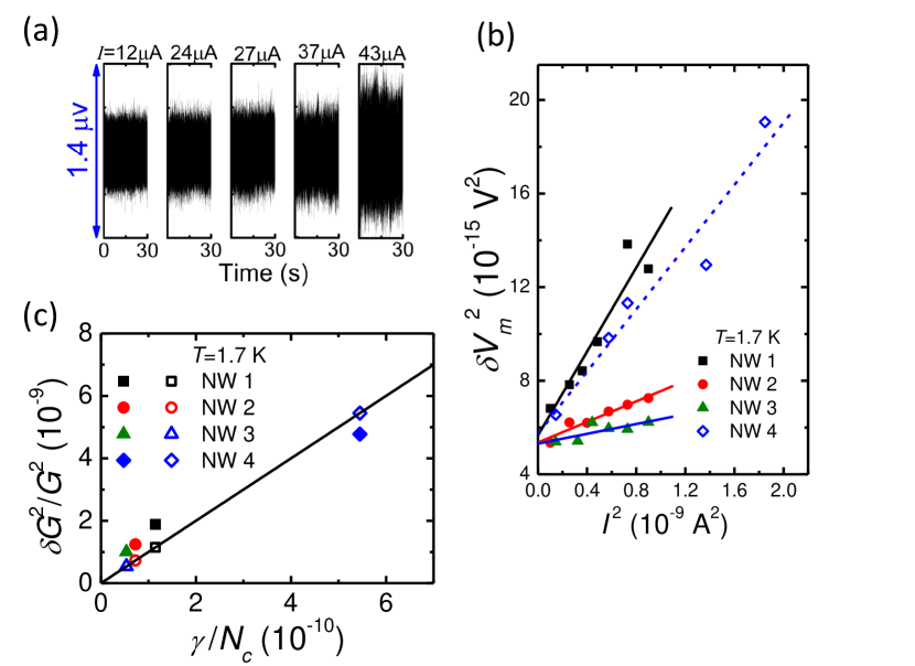
In our experimental method, a current is applied to the NW device and the total voltage fluctuations are measured, i.e., , where is the voltage noise of the NW, and is the input noise of the preamplifier. Figure 4(a) shows the measured at several values for NW 4 at 1.7 K. We see that the magnitude increases with increasing . The value of a NW can be obtained by subtracting out the background contribution . Because and are uncorrelated, we write for an ohmic conductor, where , , and denote the variances of , , and , respectively. Thus, the intrinsic resistance fluctuations of the NW can be obtained from a plot of versus . Figure 4(b) shows the variation of with for our NWs at 1.7 K. A linear dependence is observed for all NWs, with the fitted V2. Here we note that in our noise measurements, the sampling rate of the spectrum analyzer (Stanford Research model SR785) was set to be 1024 Hz and the measurement time was lasted for 30 s, corresponding to the relevant frequency range from Hz to Hz. This range leads to an estimated upper bound V2, being in good accord with our measurement.
Once value in each NW is obtained from the slope in Fig. 4(b), can be calculated. The calculated values (solid symbols) as a function of the normalized Hooge parameter are plotted in Fig. 4(c). Alternatively, we have calculated values (open symbols) from the measured (Fig. 2) through Eq. (2), by inserting . Figure 4(c) shows that the values obtained from the two independent methods agree to within a factor of 2. At = 1.7 K, and in NWs 1 and 4, respectively. We thus obtain 95 (81) nm in the former (the latter) through Eq. (3), where m-1.Lin et al. (1999) Therefore, we have and , justifying the application of Eq. (3).
The 1/ noise has previously been studied in a wide variety of metalsDutta and Horn (1981); Weissman (1988); Giordano (1991) and semiconductors,Fleetwood (2015) and recently, in 2D materials.Balandin (2013); Karnatak et al. (2017) UCF-induced 1/ noise were observed in polycrystalline Bi films,Birge, Golding, and Haemmerle (1989) Ag films,Meisenheimer and Giordano (1989); McConville and Birge (1993) Au wires,Trionfi, Lee, and Natelson (2007) RuO2 NWs,Lien et al. (2011) C-Cu composites,Garfunkel et al. (1988) and epitaxial graphene.Kalmbach et al. (2016) In Bi and Ag films, the UCF fell in the “unsaturated” regime where . The origins of the mobile defects were unspecified in those samples, while the diffusion of H atoms (the spin-glass freezing process) was identified as the cause in amorphous Ni-Zr filmsAlers et al. (1989) (narrow AuFe wiresNeuttiens et al. (2000)). In the present study, we are able to show that VO’s are rich and generate mobile defects in IrO2.
In summary, we have measured the 1/ noise of four IrO2 nanowires in the temperature range from 1.7 to 350 K. As temperature decreases from 350 K, the value decreases down to about 100 K and then remains constant, but as K increases with decreasing temperature. We explain this low-temperature increase in terms of the UCF-induced 1/ noise. We identify the mobile defects to be associated with oxygen vacancies in the IrO2 rutile structure. In combination with the orbital 2CK effect previously observed in this Dirac nodal line metal, we have extracted the number density of the mobile defects. The UCF origin of the 1/ noise is further confirmed by independent measurements of temporal conductance fluctuations in the nanowires.
ACKNOWLEDGMENTS
We thank C. W. Wu for experimental help. This work was supported by National Science and Technology Council of Taiwan through grant numbers 110-2112-M-A49-015 and 111-2119-M-007-005 (J.J.L.), and 110-2112-M-A49-033-MY3 (S.S.Y.).
REFERENCES
References
- Fujiwara et al. (2013) K. Fujiwara, Y. Fukuma, J. Matsuno, H. Idzuchi, Y. Niimi, Y. Otani, and H. Takagi, “5 iridium oxide as a material for spin-current detection,” Nat. Commun. 4, 2893 (2013).
- Dong et al. (2018) Q. Dong, D. Song, Y. Huang, Z. Xu, J. H. Chapman, W. S. Willis, B. Li, and Y. Lei, “High-temperature annealing enabled iridium oxide nanofibers for both non-enzymatic glucose and solid-state pH sensing,” Electrochim. Acta 281, 117 (2018).
- Yeh et al. (2020) S. S. Yeh, T. K. Su, A. S. Lien, F. Zamani, J. Kroha, C. C. Liao, S. Kirchner, and J. J. Lin, “Oxygen vacancy-driven orbital multichannel kondo effect in dirac nodal line metals IrO2 and RuO2,” Nat. Commun. 11, 4749 (2020).
- Kirchner (2020) S. Kirchner, “Two-channel Kondo physics: From engineered structures to quantum materials realizations,” Adv. Quantum Technol. 3, 1900128 (2020).
- Balandin (2013) A. A. Balandin, “Low-frequency noise in graphene devices,” Nat. Nanotechnol. 8, 549 (2013).
- Dutta and Horn (1981) P. Dutta and P. M. Horn, “Low-frequency fluctuations in solids: noise,” Rev. Mod. Phys. 53, 497 (1981).
- Weissman (1988) M. B. Weissman, “ noise and other slow, nonexponential kinetics in condensed matter,” Rev. Mod. Phys. 60, 537 (1988).
- Fleetwood (2015) D. M. Fleetwood, “ noise and defects in microelectronic materials and devices,” IEEE Trans. Nucl. Sci. 62, 1462 (2015).
- Giordano (1991) N. Giordano, “Conductance fluctuations and low-frequency noise in small disordered systems: experiment,” in Mesoscopic Phenomena in Solids, edited by B. L. Altshuler, P. A. Lee, and R. A. Webb (Elsevier, New York, 1991).
- Feng (1991) S. Feng, “Conductance fluctuations and noise magnitudes in small disordered structures: theory,” in Mesoscopic Phenomena in Solids, edited by B. L. Altshuler, P. A. Lee, and R. A. Webb (Elsevier, New York, 1991).
- Gupta (1994) M. S. Gupta, “Conductance fluctuations in mesoscopic conductors at low temperatures,” IEEE Trans. Electron Devices 41, 2093 (1994).
- Chen et al. (2004a) R. S. Chen, Y. S. Huang, Y. M. Liang, C. S. Hsieh, D. S. Tsai, and K. K. Tiong, “Field emission from vertically aligned conductive IrO2 nanorods,” Appl. Phys. Lett. 84, 1552 (2004a).
- Lin et al. (2008) Y. H. Lin, Y. C. Sun, W. B. Jian, H. M. Chang, Y. S. Huang, and J. J. Lin, “Electrical transport studies of individual IrO2 nanorods and their nanorod contacts,” Nanotechnology 19, 045711 (2008).
- Chen et al. (2004b) R. Chen, H. Chang, Y. Huang, D. Tsai, S. Chattopadhyay, and K. Chen, “Growth and characterization of vertically aligned self-assembled IrO2 nanotubes on oxide substrates,” J. Cryst. Growth 271, 105 (2004b).
- Scofield (1987) J. H. Scofield, “ac method for measuring low-frequency resistance fluctuation spectra,” Rev. Sci. Instrum. 58, 985 (1987).
- Hooge (1969) F. Hooge, “ noise is no surface effect,” Phys. Lett. A 29, 139 (1969).
- Kawasaki et al. (2018) J. K. Kawasaki, C. H. Kim, J. N. Nelson, S. Crisp, C. J. Zollner, E. Biegenwald, J. T. Heron, C. J. Fennie, D. G. Schlom, and K. M. Shen, “Engineering carrier effective masses in ultrathin quantum wells of IrO2,” Phys. Rev. Lett. 121, 176802 (2018).
- Pelz and Clarke (1987) J. Pelz and J. Clarke, “Quantitative "local-interference" model for noise in metal films,” Phys. Rev. B 36, 4479 (1987).
- Lin and Bird (2002) J. J. Lin and J. P. Bird, “Recent experimental studies of electron dephasing in metal and semiconductor mesoscopic structures,” J. Phys.: Condens. Matter 14, R501 (2002).
- Yang et al. (2012) P. Y. Yang, L. Y. Wang, Y. W. Hsu, and J. J. Lin, “Universal conductance fluctuations in indium tin oxide nanowires,” Phys. Rev. B 85, 085423 (2012).
- Zhong et al. (2010) Y. L. Zhong, A. Sergeev, C. D. Chen, and J. J. Lin, “Direct observation of electron dephasing due to inelastic scattering from defects in weakly disordered AuPd wires,” Phys. Rev. Lett. 104, 206803 (2010).
- Zhong and Lin (1998) Y. L. Zhong and J. J. Lin, “Observation of a linear mean-free-path dependence of the electron-phonon scattering rate in thick AuPd films,” Phys. Rev. Lett. 80, 588 (1998).
- Trionfi, Lee, and Natelson (2007) A. Trionfi, S. Lee, and D. Natelson, “Time-dependent universal conductance fluctuations in mesoscopic Au wires: Implications,” Phys. Rev. B 75, 104202 (2007).
- Lee and Ramakrishnan (1985) P. A. Lee and T. V. Ramakrishnan, “Disordered electronic systems,” Rev. Mod. Phys. 57, 287 (1985).
- Affleck and Ludwig (1993) I. Affleck and A. W. W. Ludwig, “Exact conformal-field-theory results on the multichannel Kondo effect: Single-fermion green’s function, self-energy, and resistivity,” Phys. Rev. B 48, 7297 (1993).
- Lin et al. (1999) J. J. Lin, W. Xu, Y. L. Zhong, J. H. Huang, and Y. S. Huang, “Electron-electron scattering times in low-diffusivity thick RuO2 and IrO2 films,” Phys. Rev. B 59, 344 (1999).
- Yeh et al. (2018) S. S. Yeh, K. H. Gao, T. L. Wu, T. K. Su, and J. J. Lin, “Activation energy distribution of dynamical structural defects in RuO2 films,” Phys. Rev. Appl. 10, 034004 (2018).
- Birge, Golding, and Haemmerle (1989) N. O. Birge, B. Golding, and W. H. Haemmerle, “Electron quantum interference and noise in bismuth,” Phys. Rev. Lett. 62, 195 (1989).
- Hewson (1993) A. C. Hewson, The Kondo Problem to Heavy Fermions (Cambridge University Press, Cambridge, 1993).
- Chakravarty and Nayak (2000) S. Chakravarty and C. Nayak, “A Kondo impurity in a disordered metal: Anderson’s theorem revisited,” Int. J. Mod. Phys. B 14, 1421 (2000).
- Lin et al. (2004) J. J. Lin, S. M. Huang, Y. H. Lin, T. C. Lee, H. Liu, X. X. Zhang, R. S. Chen, and Y. S. Huang, “Low temperature electrical transport properties of RuO2 and IrO2 single crystals,” J. Phys. Condens. Matter 16, 8035 (2004).
- Feng, Lee, and Stone (1986) S. Feng, P. A. Lee, and A. D. Stone, “Sensitivity of the conductance of a disordered metal to the motion of a single atom: Implications for noise,” Phys. Rev. Lett. 56, 1960 (1986).
- Karnatak et al. (2017) P. Karnatak, T. Paul, S. Islam, and A. Ghosh, “ noise in van der Waals materials and hybrids,” Adv. Phys.: X 2, 428 (2017).
- Meisenheimer and Giordano (1989) T. L. Meisenheimer and N. Giordano, “Conductance fluctuations in thin silver films,” Phys. Rev. B 39, 9929 (1989).
- McConville and Birge (1993) P. McConville and N. O. Birge, “Weak localization, universal conductance fluctuations, and noise in Ag,” Phys. Rev. B 47, 16667 (1993).
- Lien et al. (2011) A. S. Lien, L. Y. Wang, C. S. Chu, and J. J. Lin, “Temporal universal conductance fluctuations in RuO2 nanowires due to mobile defects,” Phys. Rev. B 84, 155432 (2011).
- Garfunkel et al. (1988) G. A. Garfunkel, G. B. Alers, M. B. Weissman, J. M. Mochel, and D. J. VanHarlingen, “Universal-conductance-fluctuation noise in a metal-insulator composite,” Phys. Rev. Lett. 60, 2773 (1988).
- Kalmbach et al. (2016) C. C. Kalmbach, F. J. Ahlers, J. Schurr, A. Müller, J. Feilhauer, M. Kruskopf, K. Pierz, F. Hohls, and R. J. Haug, “Nonequilibrium mesoscopic conductance fluctuations as the origin of noise in epitaxial graphene,” Phys. Rev. B 94, 205430 (2016).
- Alers et al. (1989) G. B. Alers, M. B. Weissman, R. S. Averback, and H. Shyu, “Resistance noise in amorphous Ni-Zr: Hydrogen diffusion and universal conductance fluctuations,” Phys. Rev. B 40, 900–906 (1989).
- Neuttiens et al. (2000) G. Neuttiens, C. Strunk, C. Van Haesendonck, and Y. Bruynseraede, “Universal conductance fluctuations and low-temperature noise in mesoscopic AuFe spin glasses,” Phys. Rev. B 62, 3905 (2000).