Second Quantization: Gating a Quantum Dot Through the Sequential Removal of Single Electrons from a Nanoscale Floating Gate
Abstract
We use the tip of an atomic force microscope (AFM) to charge floating metallic gates defined on the surface of a Si/SiGe heterostructure. The AFM tip serves as an ideal and movable cryogenic switch, allowing us to bias a floating gate to a specific voltage and then lock the charge on the gate by withdrawing the tip. Biasing with an AFM tip allows us to reduce the size of a quantum dot floating gate electrode down to . Measurements of the conductance through a quantum dot formed beneath the floating gate indicate that its charge changes in discrete steps. From the statistics of the single-electron leakage events, we determine the floating gate leakage resistance - a value immeasurable by conventional means.
I Introduction
Spin qubits in gate-defined quantum dots (QDs) have recently demonstrated two qubit gates with fidelities exceeding fault-tolerant thresholds [1, 2, 3]. Spin qubits have also been integrated with microwave cavities, enabling dispersive spin state readout, coherent spin-photon coupling, and microwave-mediated spin-spin interactions [4, 5, 6, 7, 8]. Long coherence times [9], compatibility with industrial fabrication techniques [10, 11], and the potential for integration with classical silicon electronics [12] make them one of the most promising platforms for quantum computing [13, 14].
As quantum processors increase in complexity, many solid state qubit platforms will soon face the challenge of delivering a growing number of room temperature control signals to the cryogenic environment of the chip. Since most quantum error correction protocols require qubits to be arranged in two-dimensional (2D) arrays [15], qubit interconnect crowding is an outstanding issue [16]. For semiconductor spin qubits, where qubits are only separated by 100 nm, the interconnect challenge is further exacerbated [17, 18].
A primary approach that is being pursued to reduce the number of room temperature control lines is charge-locking [19, 20, 21]. Charge locking is conceptually related to classical dynamic random access memory [22]. In the case of gate-defined QDs, the concept is to electrically detach the QD gate electrode from the control line. If the electrical isolation of the gate is high, it will retain its charge for a sufficiently long time, allowing other gates on the device to be manipulated with the same room temperature control line. In the perfect case, the so-called “sample-and-hold” circuit [23], a zero-resistance switch is desired to dynamically charge and lock the floating node as shown in Fig. 1(a). Practically it is quite challenging to realize a mechanical switch for mesoscopic devices. To date only field-effect transistors (FETs), integrated both on-chip and off-chip, have been used to isolate gates from room temperature signals in GaAs [21, 24], Si/SiGe [25, 26], and CMOS [27, 28] QDs.
Interconnect crowding in 2D qubit arrays can be significantly eased by vertically bringing electrical connections out of the device plane. Air bridges [29] and thru-silicon vias with indium bumps have been successfully implemented for superconducting qubits [30, 31]. Flip-chip bonding is being pursued for cavity-coupled Si spin qubits [32]. A CMOS-compatible device architecture incorporating nanoscale vias was recently introduced [33], but its application has so far been limited to small linear arrays of Si/SiGe QDs [34].
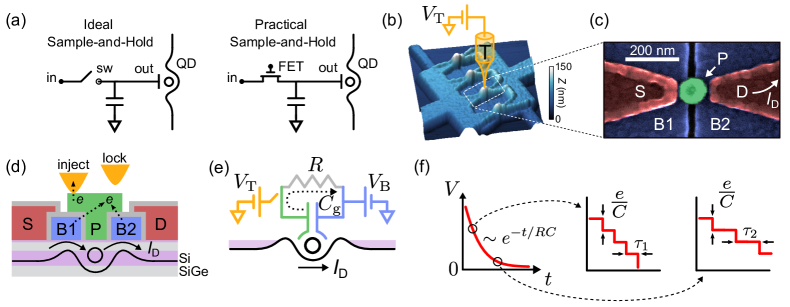
Inspired by the potential of via-based 3D integration [33, 34], we explore the nanoscale limit of the floating gate approach by fabricating isolated gates with diameter . We attempt to realize the ideal sample-and-hold circuit by using the tip of an atomic force microscope (AFM) as a movable voltage node [35, 36]. The floating gate can then be electrically charged by contacting it with a voltage-biased AFM tip. Withdrawing the AFM tip locks the charge on the floating gate. We probe the charge retention of the floating gate by measuring the conductance through a QD defined in a Si quantum well beneath the floating gate. The true floating gate design and its small 100 nm diameter eliminates problems typical for FET-based charge-locking, such as charge leaking through the FET channel due to a finite on-off ratio [27].
We first demonstrate that the AFM tip can be used as a stationary vertical gate while in continuous electrical contact with the metallic floating gate. By sweeping the dc tip voltage, , we can tune the QD charge occupancy as in a conventional QD device. Then, by withdrawing the biased tip, we show that the electric charge is locked on the floating gate over a time-scale set by the leakage resistance to other gates on the device. We confirm the non-destructive character of the injection/locking process by repeating it multiple times on a single gate and obtaining a reproducible charge-sensor response down to individual electron tunneling events.
The nanoscale dimensions of our floating gate allows us to explore an intriguing “second quantized” operating regime since the voltage resolution of the gate is fundamentally limited by the quantization of electric charge [37]. Due to a sub-fF total capacitance of the gate, only a few hundred electrons have to be removed from the gate to induce a few-electron QD beneath it. In addition, we directly probe the retention time of the charge locked on the floating gate. We utilize the QD induced in the quantum well under the floating gate as a highly sensitive charge sensor [38, 39] to extract values of and . In devices with a single layer of gates, we show that charge can stay locked for several hours.
II Experimental setup
Our accumulation-mode device is fabricated on an undoped Si/SiGe heterostructure consisting of a thick Si quantum well (QW) that is buried under a thick layer of Si0.7Ge0.3 and a thick Si cap. To form a QD in the plane of the QW, we utilize a gate stack consisting of three overlapping layers as shown in Figs. 1(c,d). Two Al layers form barrier (B1, B2) and accumulation (S, D) gates, while the Pd disc on top serves as a floating plunger gate. Pd is used for the final layer as it enables good electric contact to the AFM tip [40]. In this work we focus on a small section of the device, indicated by the white dashed line in Fig. 1(b), while other sections of the device show similar behavior.
During charge injection [Fig. 1(d)], the tip stays in contact with the floating gate and . Charge-locking takes place when the biased tip is lifted away from the device ( above the gate). After the AFM tip is extracted, the charge trapped on the floating gate can leak to the Si/SiGe substrate or the Al barrier gates (B1, B2). We measure the current through the QD induced beneath the P-gate to sense the real-time dynamics of the locked charge. The equivalent circuit is shown in Fig. 1(e) where the switch denotes the tip, while the tunnel junction between the floating gate and barriers is depicted as an circuit capacitively coupled to the Si/SiGe QD.
In a classical discharging circuit, the time constant can be extracted from the exponential decay of voltage across the capacitor as shown in the left panel of Fig. 1(f). However, the individual values of and remain unknown. Nevertheless, and can be extracted independently if the electrometer is sensitive and fast enough to resolve single electron tunneling events, as sketched in Fig. 1(f) [41]. The capacitance is directly related to the size of the discrete voltage steps . At the same time the resistance can be extracted from the electric current , where is the average waiting time before the next tunneling event. Note that in this model increases linearly as decreases.
III AFM-based charge-locking
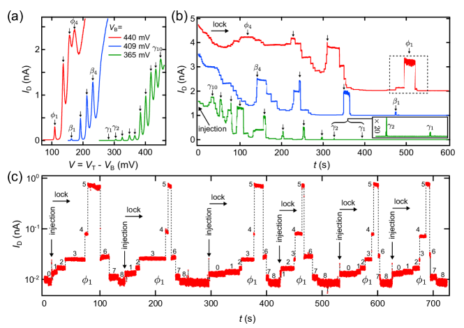
We begin by measuring Coulomb peaks with the tip in contact with the floating gate, such that = . Figure 2(a) shows through the QD induced in the QW as a function of the voltage difference between the floating gate and barrier gates . For these experiments the barrier gates are kept at the same potential = = . Three traces are acquired with different to cover a broader range of and . We mark each visible Coulomb peak: , and for the red, blue, and green curves respectively.
By suddenly lifting the tip from the floating gate and monitoring , we study the retention of the locked charge for three values of as shown in Fig. 2(b). These data sets are color-matched to a corresponding curve in Fig. 2(a). Just before the tip was lifted around (injection), for each curve was slightly exceeding the last prominent CBP in Fig. 2(a) (, and ). As time passes, the floating gate discharges and retraces the series of Coulomb peaks shown in Fig. 2(a). In contrast to continuous injection, where the AFM tip is in contact with the floating gate, discharge occurs in discrete steps. In Fig. 2(c), we show that single-electron tunneling is the dominant process here and the jumps are solely related to the electrostatic environment around the QD and are not just random measurements artifacts due to noise. Here we sequentially repeat injection and locking of charge around the CBP , as highlighted by the dashed square in Fig. 2(b). After each injection, the current evolves through the same sequence of discrete steps marked from 0 to 8, the number of additional electrons that have tunneled to the floating gate. The reproducibility of the plateaus in implies that the rates of all higher-order tunneling processes are much slower. Note that we work at differential voltages that are much larger than the superconducting gap of Al. However, very rarely [e.g. for 2 out of 50 events in Fig. 2(c)], the waiting time between two tunneling events appears to be shorter than the integration time () making these events indistinguishable from two-electron tunneling. As a result, the measured total capacitance of the floating gate, which can be extracted directly from the time traces [42] as described below, acquires imprecision due to these counting errors.
IV Capacitance measurement by counting electrons
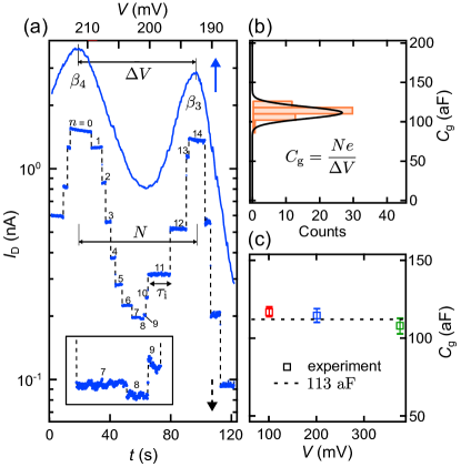
In Fig. 3(a) we plot side-by-side the pair of CBPs and [marked by blue shading in Figs. 2(a, b)] as a function of (top axis) and time (bottom axis). For clarity, the upper data set is offset by 1 nA. The voltage difference between the peaks can be alternatively covered by electrons tunneling to the floating gate such that . By definition the total capacitance can be measured through single electron counting. We repeat the injection-locking cycle multiple times for three different differential voltages between and , and , and and from Figs. 2(a, b) and plot the histogram of measured ’s in Fig. 3(b). The narrow distribution implies a single dominant tunneling process, which is slightly widened towards lower capacitance by two-electron processes and towards higher capacitance by large charge noise events that are interpreted as electron tunneling events.
The extracted is plotted as a function of differential voltage in Fig. 3(c). As expected, shows no dependence on since the capacitance is determined only by the device geometry. The error in originates from both the confidence interval of the mean value in Fig. 3(b) and from the systematic one-electron uncertainty between and . It should be noted that the measured value is the total capacitance of the floating gate, which can be further broken into the sum of tunnel junction (TJ) and floating gate-to-QD capacitances: . The latter can be estimated simply as .
AFM-based charge locking allows us to reduce the footprint and stray capacitance of the floating node by a factor of 700 – 7000 compared to previous FET-based experiments [27, 26]. From a metrological perspective, our approach allows a direct measurement of the sub-fF total capacitance of an isolated object by counting electrons using a QD charge sensor. In previous work [42], the capacitance standard based on counting electrons was 16,000 larger.
V Tunneling statistics and resistance
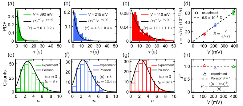
From time traces similar to the one shown in Fig. 3(a), we can directly extract the statistical properties of sequential electron transport to the floating gate [39] and confirm it’s uncorrelated nature. In Figs. 4(a–c), we plot probability density functions (PDF) of the waiting time distribution between adjacent tunneling events at various differential voltages. As expected for the uncorrelated transport of particles through the highly non-transparent TJ [43], the waiting times are distributed exponentially [44] , where is the mean time interval between tunneling events. Additionally, we can extract the time correlation transport properties as shown in Figs. 4(e–g). Here we plot the distribution of the number of events during a given time window , which is chosen to fit roughly the same average number of events . We checked that this choice does not affect the results. The theoretical Poisson distributions (solid lines) , where the occurrence rate is determined experimentally by the mean time, match the experimental data very well, given that no fitting parameters are used. The second central moment (shot-noise) of the distribution , known as the Fano factor [44] closely fits the tunnel junction limit [43, 45] as shown in Fig. 4(h).
The extracted mean time interval between tunneling events can be converted [46] to the average electrical current , plotted in Fig. 4(d) as a function of differential voltage. The resulting curve originates at the origin, confirming the statement that the charge leaks solely through the barrier gates. From the linear fit, we can extract the resistance of the TJ: . Such a high value is immeasurable by conventional means and the FET-based charge locking technique. The latter is because even a lower estimate of the typical FET stray capacitance of [26, 28] i) results in an almost infinite time constant (taking the data for Fig. 4(d) would have taken months) and ii) the QD sensor must be highly sensitive to catch voltage jumps of . We addressed this limitation by dramatically reducing the stray capacitance of the floating gate (1000 times) to achieve a feasible time constant of .
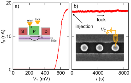
To cross-check our findings about the origin of the charge leakage in multilayer devices, we fabricated a single-layer device. Here, seven floating gates sit strictly on the Si/SiGe substrate, which now is the only path for charge to leak. Since all floating gates behave similarly, we present charge retention data from one of them, as shown in the inset of Fig. 5(b).
We start in the continuous injection mode sketched in Fig. 5(a), when the tip constantly touches the floating gate. As before, we measure the current between the two ohmic contacts under the wide accumulation gates while applying a positive voltage to the floating gate. The transistor-like turn-on curve shown in Fig. 5(a) lacks Coulomb oscillations due to the limited control of the confinement potential in single layer devices. Figure 5(a) shows the current measured as a function of time after the charge was locked with . In contrast to the multilayer device data presented above, we do not observe any charge leakage or tunneling events over several hours. As expected, the tunneling rate to the Si substrate is orders of magnitudes slower than the tunneling rate between overlapping gate layers.
VI Conclusion and outlook
In conclusion, we realized the ideal sample-and-hold circuit with a floating metallic gate fabricated on the surface of a Si/SiGe heterostucture. Utilizing the AFM tip as a switch allows us to reduce the plunger gate footprint down to 100 nm. The resulting stray capacitance of the floating gate is 2–3 orders of magnitude lower than in previous FET-based charge locking studies. The reduction of the stray capacitance allows us to probe much higher junction resistances through single electron counting than in previous studies. We find the average gate discharge tunneling rate to be of the order of one electron every few seconds in the overlapping gate architecture and multiple hours for single-layer devices. It follows that single-layer floating gates that do not require fast operation, such as those defining charge sensors, could be biased using the sample-and-hold approach, thereby significantly reducing the number of room temperature control lines per qubit. Looking forward, the AFM charging approach demonstrated here could be combined with tip-based dispersive readout [47], enabling us to in-situ tune and drag tip-induced QDs across the chip [48].
Acknowledgements.
Supported by Army Research Office grant W911NF-15-1-0149 and the Gordon and Betty Moore Foundation’s EPiQS Initiative through Grant No. GBMF4535. The authors thank V. Khrapai, M. F. Gonzalez-Zalba and A. Sachrajda for useful discussions. The authors thank F. Borjans and A. Mills for technical contributions to device fabrication and HRL Laboratories for providing the Si/SiGe heterostructures.References
- Mills et al. [2022] A. R. Mills, C. R. Guinn, M. J. Gullans, A. J. Sigillito, M. M. Feldman, E. Nielsen, and J. R. Petta, Two-qubit silicon quantum processor with operation fidelity exceeding 99%, Sci. Adv. 8, eabn5130 (2022).
- Xue et al. [2022] X. Xue, M. Russ, N. Samkharadze, B. Undseth, A. Sammak, G. Scappucci, and L. M. K. Vandersypen, Quantum logic with spin qubits crossing the surface code threshold, Nature 601, 343 (2022).
- Noiri et al. [2022] A. Noiri, K. Takeda, T. Nakajima, T. Kobayashi, A. Sammak, G. Scappucci, and S. Tarucha, Fast universal quantum gate above the fault-tolerance threshold in silicon, Nature 601, 338 (2022).
- Mi et al. [2018] X. Mi, M. Benito, S. Putz, D. M. Zajac, J. M. Taylor, G. Burkard, and J. R. Petta, A coherent spin–photon interface in silicon, Nature 555, 599 (2018).
- Landig et al. [2018] A. J. Landig, J. V. Koski, P. Scarlino, U. C. Mendes, A. Blais, C. Reichl, W. Wegscheider, A. Wallraff, K. Ensslin, and T. Ihn, Coherent spin–photon coupling using a resonant exchange qubit, Nature 560, 179 (2018).
- Samkharadze et al. [2018] N. Samkharadze, G. Zheng, N. Kalhor, D. Brousse, A. Sammak, U. C. Mendes, A. Blais, G. Scappucci, and L. M. K. Vandersypen, Strong spin-photon coupling in silicon, Science 359, 1123 (2018).
- Borjans et al. [2020] F. Borjans, X. G. Croot, X. Mi, M. J. Gullans, and J. R. Petta, Resonant microwave-mediated interactions between distant electron spins, Nature 577, 195 (2020).
- Harvey-Collard et al. [2022] P. Harvey-Collard, J. Dijkema, G. Zheng, A. Sammak, G. Scappucci, and L. M. K. Vandersypen, Coherent spin-spin coupling mediated by virtual microwave photons, Phys. Rev. X 12, 021026 (2022).
- Tyryshkin et al. [2012] A. M. Tyryshkin, S. Tojo, J. J. L. Morton, H. Riemann, N. V. Abrosimov, P. Becker, H.-J. Pohl, T. Schenkel, M. L. W. Thewalt, K. M. Itoh, and S. A. Lyon, Electron spin coherence exceeding seconds in high-purity silicon, Nat. Mater. 11, 143 (2012).
- Maurand et al. [2016] R. Maurand, X. Jehl, D. Kotekar-Patil, A. Corna, H. Bohuslavskyi, R. Laviéville, L. Hutin, S. Barraud, M. Vinet, M. Sanquer, and S. De Franceschi, A CMOS silicon spin qubit, Nat. Commun. 7, 13575 (2016).
- Zwerver et al. [2022] A. M. J. Zwerver, T. Krähenmann, T. F. Watson, L. Lampert, H. C. George, R. Pillarisetty, S. A. Bojarski, P. Amin, S. V. Amitonov, J. M. Boter, R. Caudillo, D. Correas-Serrano, J. P. Dehollain, G. Droulers, E. M. Henry, R. Kotlyar, M. Lodari, F. Lüthi, D. J. Michalak, B. K. Mueller, S. Neyens, J. Roberts, N. Samkharadze, G. Zheng, O. K. Zietz, G. Scappucci, M. Veldhorst, L. M. K. Vandersypen, and J. S. Clarke, Qubits made by advanced semiconductor manufacturing, Nat. Electron. 5, 184 (2022).
- Xue et al. [2021] X. Xue, B. Patra, J. P. G. van Dijk, N. Samkharadze, S. Subramanian, A. Corna, B. Paquelet Wuetz, C. Jeon, F. Sheikh, E. Juarez-Hernandez, B. P. Esparza, H. Rampurawala, B. Carlton, S. Ravikumar, C. Nieva, S. Kim, H.-J. Lee, A. Sammak, G. Scappucci, M. Veldhorst, F. Sebastiano, M. Babaie, S. Pellerano, E. Charbon, and L. M. K. Vandersypen, CMOS-based cryogenic control of silicon quantum circuits, Nature 593, 205 (2021).
- Loss and DiVincenzo [1998] D. Loss and D. P. DiVincenzo, Quantum computation with quantum dots, Phys. Rev. A 57, 120 (1998).
- Burkard et al. [ress] G. Burkard, T. D. Ladd, J. M. Nichol, A. Pan, and J. R. Petta, Semiconductor spin qubits, Rev. Mod. Phys. (in press).
- Fowler et al. [2012] A. G. Fowler, M. Mariantoni, J. M. Martinis, and A. N. Cleland, Surface codes: Towards practical large-scale quantum computation, Phys. Rev. A 86, 032324 (2012).
- Borsoi et al. [2022] F. Borsoi, N. W. Hendrickx, V. John, S. Motz, F. van Riggelen, A. Sammak, S. L. de Snoo, G. Scappucci, and M. Veldhorst, Shared control of a 16 semiconductor quantum dot crossbar array, (2022), arXiv:2209.06609 .
- Zajac et al. [2015] D. M. Zajac, T. M. Hazard, X. Mi, K. Wang, and J. R. Petta, A reconfigurable gate architecture for Si/SiGe quantum dots, Appl. Phys. Lett. 106, 223507 (2015).
- Zajac et al. [2016] D. M. Zajac, T. M. Hazard, X. Mi, E. Nielsen, and J. R. Petta, Scalable gate architecture for a one-dimensional array of semiconductor spin qubits, Phys. Rev. Applied 6, 054013 (2016).
- Vandersypen et al. [2017] L. M. K. Vandersypen, H. Bluhm, J. S. Clarke, A. S. Dzurak, R. Ishihara, A. Morello, D. J. Reilly, L. R. Schreiber, and M. Veldhorst, Interfacing spin qubits in quantum dots and donors—hot, dense, and coherent, npj Quantum Inf. 3, 34 (2017).
- Veldhorst et al. [2017] M. Veldhorst, H. G. J. Eenink, C. H. Yang, and A. S. Dzurak, Silicon CMOS architecture for a spin-based quantum computer, Nat. Commun. 8, 1766 (2017).
- Pauka et al. [2019] S. J. Pauka, K. Das, R. Kalra, A. Moini, Y. Yang, M. Trainer, A. Bousquet, C. Cantaloube, N. Dick, G. C. Gardner, M. J. Manfra, and D. J. Reilly, A cryogenic interface for controlling many qubits (2019), arXiv:1912.01299 .
- Keeth et al. [2007] B. Keeth, R. J. Baker, B. Johnson, and F. Lin, DRAM Circuit Design: Fundamental and High-Speed Topics, (2007).
- Horowitz and Hill [2015] P. Horowitz and W. Hill, The art of electronics; 3rd ed. (Cambridge University Press, Cambridge, 2015).
- Puddy et al. [2015] R. K. Puddy, L. W. Smith, H. Al-Taie, C. H. Chong, I. Farrer, J. P. Griffiths, D. A. Ritchie, M. J. Kelly, M. Pepper, and C. G. Smith, Multiplexed charge-locking device for large arrays of quantum devices, Appl. Phys. Lett. 107, 143501 (2015).
- Ward et al. [2013] D. R. Ward, D. E. Savage, M. G. Lagally, S. N. Coppersmith, and M. A. Eriksson, Integration of on-chip field-effect transistor switches with dopantless Si/SiGe quantum dots for high-throughput testing, Appl. Phys. Lett. 102, 213107 (2013).
- Xu et al. [2020] Y. Xu, F. K. Unseld, A. Corna, A. M. J. Zwerver, A. Sammak, D. Brousse, N. Samkharadze, S. V. Amitonov, M. Veldhorst, G. Scappucci, R. Ishihara, and L. M. K. Vandersypen, On-chip integration of Si/SiGe-based quantum dots and switched-capacitor circuits, Appl. Phys. Lett. 117, 144002 (2020).
- Schaal et al. [2018] S. Schaal, S. Barraud, J. J. L. Morton, and M. F. Gonzalez-Zalba, Conditional Dispersive Readout of a CMOS Single-Electron Memory Cell, Phys. Rev. Applied 9, 054016 (2018).
- Schaal et al. [2019] S. Schaal, A. Rossi, V. N. Ciriano-Tejel, T.-Y. Yang, S. Barraud, J. J. L. Morton, and M. F. Gonzalez-Zalba, A CMOS dynamic random access architecture for radio-frequency readout of quantum devices, Nat. Electron. 2, 236 (2019).
- Chen et al. [2014] Z. Chen, A. Megrant, J. Kelly, R. Barends, J. Bochmann, Y. Chen, B. Chiaro, A. Dunsworth, E. Jeffrey, J. Y. Mutus, P. J. J. O’Malley, C. Neill, P. Roushan, D. Sank, A. Vainsencher, J. Wenner, T. C. White, A. N. Cleland, and J. M. Martinis, Fabrication and characterization of aluminum airbridges for superconducting microwave circuits, Appl. Phys. Lett. 104, 052602 (2014).
- Rosenberg et al. [2017] D. Rosenberg, D. Kim, R. Das, D. Yost, S. Gustavsson, D. Hover, P. Krantz, A. Melville, L. Racz, G. O. Samach, S. J. Weber, F. Yan, J. L. Yoder, A. J. Kerman, and W. D. Oliver, 3D integrated superconducting qubits, npj Quantum Inf. 3, 42 (2017).
- Mallek et al. [2021] J. L. Mallek, D.-R. W. Yost, D. Rosenberg, J. L. Yoder, G. Calusine, M. Cook, R. Das, A. Day, E. Golden, D. K. Kim, J. Knecht, B. M. Niedzielski, M. Schwartz, A. Sevi, C. Stull, W. Woods, A. J. Kerman, and W. D. Oliver, Fabrication of superconducting through-silicon vias, (2021), arXiv:2103.08536 .
- Holman et al. [2021] N. Holman, D. Rosenberg, D. Yost, J. L. Yoder, R. Das, W. D. Oliver, R. McDermott, and M. A. Eriksson, 3D integration and measurement of a semiconductor double quantum dot with a high-impedance TiN resonator, npj Quantum Inf. 7, 137 (2021).
- Ha et al. [2022] W. Ha, S. D. Ha, M. D. Choi, Y. Tang, A. E. Schmitz, M. P. Levendorf, K. Lee, J. M. Chappell, T. S. Adams, D. R. Hulbert, E. Acuna, R. S. Noah, J. W. Matten, M. P. Jura, J. A. Wright, M. T. Rakher, and M. G. Borselli, A Flexible Design Platform for Si/SiGe Exchange-Only Qubits with Low Disorder, Nano Lett. 22, 1443 (2022).
- Weinstein et al. [ress] A. J. Weinstein, M. D. Reed, A. M. Jones, R. W. Andrews, D. Barnes, J. Z. Blumoff, L. E. Euliss, K. Eng, B. Fong, S. D. Ha, R. R. Hulbert, C. Jackson, M. Jura, T. E. Keating, J. Kerckhoff, A. A. Kiselev, J. Matten, G. Sabbir, A. Smith, J. Wright, M. T. Rakher, T. D. Ladd, and M. G. Borselli, Universal logic with encoded spin qubits in silicon, Nature (in press), arXiv:2202.03605 .
- Oh et al. [2021] S. W. Oh, A. O. Denisov, P. Chen, and J. R. Petta, Cryogen-free scanning gate microscope for the characterization of Si/Si0.7Ge0.3 quantum devices at milli-Kelvin temperatures, AIP Adv. 11, 125122 (2021).
- Denisov et al. [2022] A. O. Denisov, S. W. Oh, G. Fuchs, A. R. Mills, P. Chen, C. R. Anderson, M. F. Gyure, A. W. Barnard, and J. R. Petta, Microwave-Frequency Scanning Gate Microscopy of a Si/SiGe Double Quantum Dot, Nano Lett. 22, 4807 (2022).
- Guo et al. [1997] L. Guo, E. Leobandung, and S. Y. Chou, A silicon single-electron transistor memory operating at room temperature, Science 275, 649 (1997).
- Lu et al. [2003] W. Lu, Z. Ji, L. Pfeiffer, K. W. West, and A. J. Rimberg, Real-time detection of electron tunnelling in a quantum dot, Nature 423, 422 (2003).
- Gustavsson et al. [2006] S. Gustavsson, R. Leturcq, B. Simovič, R. Schleser, T. Ihn, P. Studerus, K. Ensslin, D. C. Driscoll, and A. C. Gossard, Counting statistics of single electron transport in a quantum dot, Phys. Rev. Lett. 96, 076605 (2006).
- le Sueur et al. [2008] H. le Sueur, P. Joyez, H. Pothier, C. Urbina, and D. Esteve, Phase controlled superconducting proximity effect probed by tunneling spectroscopy, Phys. Rev. Lett. 100, 197002 (2008).
- Gustavsson et al. [2009] S. Gustavsson, R. Leturcq, M. Studer, I. Shorubalko, T. Ihn, K. Ensslin, D. Driscoll, and A. Gossard, Electron counting in quantum dots, Surf. Sci. Rep. 64, 191 (2009).
- Keller et al. [1999] M. W. Keller, A. L. Eichenberger, J. M. Martinis, and N. M. Zimmerman, A capacitance standard based on counting electrons, Science 285, 1706 (1999).
- Birk et al. [1995] H. Birk, M. J. M. de Jong, and C. Schönenberger, Shot-noise suppression in the single-electron tunneling regime, Phys. Rev. Lett. 75, 1610 (1995).
- Blanter and Büttiker [2000] Y. Blanter and M. Büttiker, Shot noise in mesoscopic conductors, Phys. Rep. 336, 1 (2000).
- Spietz et al. [2003] L. Spietz, K. W. Lehnert, I. Siddiqi, and R. J. Schoelkopf, Primary electronic thermometry using the shot noise of a tunnel junction, Science 300, 1929 (2003).
- Pioro-Ladrière et al. [2005] M. Pioro-Ladrière, J. H. Davies, A. R. Long, A. S. Sachrajda, L. Gaudreau, P. Zawadzki, J. Lapointe, J. Gupta, Z. Wasilewski, and S. Studenikin, Origin of switching noise in lateral gated devices, Phys. Rev. B 72, 115331 (2005).
- Vigneau et al. [2022] F. Vigneau, F. Fedele, A. Chatterjee, D. Reilly, F. Kuemmeth, F. Gonzalez-Zalba, E. Laird, and N. Ares, Probing quantum devices with radio-frequency reflectometry, (2022), arXiv:2202.10516 .
- Shim et al. [2019] Y.-P. Shim, R. Ruskov, H. M. Hurst, and C. Tahan, Induced quantum dot probe for material characterization, Appl. Phys. Lett. 114, 152105 (2019).