Uncovering the Structural Evolution Arsenene on SiC Substrate
Abstract
Two-dimensional arsenic allotropes have been grown on metallic surfaces, while topological properties have been theoretically described on strained structures. Here we experimentally grow arsenene by molecular beam epitaxy over the insulating SiC substrate. The arsenene presents a flat structure with a strain field that follows the SiC surface periodicity. Our ab initio simulations, based on the density functional theory, corroborate the experimental observation. The strained structure presents a new arsenene allotrope with a triangular structure, rather than the honeycomb previously predicted for other pnictogens. This strained structure presents a Peierls-like transition leading to an indirect gap semiconducting behavior.
I Introduction
Strain engineering has become a powerful method to tailor atomically-thin bidimensional materials (2DMs) electronic and optical properties [1; 2; 3]. Theoretical and experimental studies have demonstrated a variety of phenomena related to the strain engineering of different 2DMs that range from the tuning of existing properties, e.g., the modulation of photoluminescence in monolayer MoS2 [4; 5; 6], up to the appearance of new or exotic effects, such as pseudo quantum Hall effect in graphene [7; 8]. All these efforts have sparked a tremendous rush for novel 2DMs exhibiting unique or enhanced properties that can be controlled by the application of an appropriate mechanical strain [1; 2; 3]. In seeking novel 2DMs that exhibit properties enabled by strain engineering, the group VA (pnictogens) has gained tremendous attention lately [9; 10; 11; 12]. In particular, monoelemental arsenic layers (arsenene) have been predicted to exhibit a phase transition from normal to topological insulator upon appropriate strain [13]. Arsenene exhibits two allotropes, namely buckled (gray arsenic phase) and puckered (black arsenic phase) layers [9]. Puckered and buckled arsenene are indirect bandgap semiconductors, with and eV bandgap, respectively [13]. Small strains have been reported to lead a transition to a direct bandgap semiconductor in puckered arsenene [13; 13], with tunable bandgap energy and effective mass upon strain variation [14]. Previous density functional theory (DFT) calculations show that tensile strains exceeding can make both arsenene polytypes behave as quantum spin hall (QSH) insulators [15]. Larger strains or , have also been claimed to allow a semiconductor-to-metallic transition in both puckered and buckled arsenene [14]. Such a large flexibility to manipulate different states and related properties of arsenene by means of strain can enable the development of a multitude of applications, including new-concept devices and quantum technologies [16].
Despite several theoretical studies on strained arsenene [15; 13; 14], experimental investigations remain very limited. Arsenene layers have been extensively produced by different methods, such as mechanical exfoliation, liquid-phase exfoliation, and chemical vapor deposition (CVD) [9], the main limitation referring to the strain application. Axial strain in 2DMs is usually applied via extrinsic methods, by using elastic substrates or controlling the 2DM thermal expansion [2; 7; 17]. These approaches are typically limited to small strains [2] and the relatively weak interactions between 2DMs and most of the substrates make the application of large extrinsic tensions very challenging.
In this paper, to tackle the challenge of producing highly strained arsenene, molecular beam epitaxy (MBE) was employed to grow arsenic onto a silicon carbide (SiC) surface. Due to the high control of the molecular beam flux and the growth temperature, MBE allows the production of high-quality 2DMs where large intrinsic strains can be achieved via the lattice mismatch between the target 2DM and the selected substrate [1]. SiC was chosen as substrate due to its high chemical and thermal stability [18; 19], and crystal structure that allows lattice mismatch induced strain with arsenene. We experimentally observed the formation of few-layer arsenene onto SiC, where the first monolayer covalently binds to the substrate, yielding an in-plane tensile strain of . The combined experimental and density functional theory results allow the interpretation of a new arsenene triangular allotrope. The ab initio calculations show the energetically favorable formation of a highly strained arsenene first layer, depicting also a decoupled nature of further arsenene layer staking. The reported system put in evidence strategies towards the development of highly strained 2DMs.
II Methods
The As deposition was carried out in a customized MBE chamber from Dr. Eberl MBE-Komponenten dedicated to growing III–V compounds. A commercial epi-polished 6H-SiC(0001) n-dopped wafer (miscut on-axis ), Si-terminated, was cleaved in pieces of mm and used as substrate. The SiC surface is characterized by nm high Si-C bilayer terraces ( nm wide), exhibiting an overall nm surface roughness (over wafer area). The SiC substrate pieces were attached to a Si wafer using eutectic gallium-indium liquid metal alloy on a holder facing down the As4 flux. To remove residual impurities from the surface, the substrate was annealed for h at C and dry-etched in an ultra-high vacuum (UHV) using a hydrogen beam. The etching procedure used a thermal cracker to source an ion-free atomic hydrogen gas beam toward the substrate surface that was heated at C and exposed to a hydrogen background pressure of mbar for min. Prior to the As epitaxial growth, the substrate was annealed at C in the deposition chamber (base pressure mbar) to remove the inert chemical H-termination and consequently uncover the SiC dangling bonds. The substrate was cooled down to C and exposed to As4 molecular beam flux. A low-temperature effusion cell was used to sublimate arsenic solid source ( purity metallic arsenic from Furukawa Denshi Co., LDT.) at C to reach the desired beam equivalent pressure (BEP) measured by a hot‑filament ionization gauge placed in front of the beam.
A thin Al capping layer was deposited in situ immediately after the arsenene growth for the analysis of the sample cross-section via an external high-resolution transmission electron microscope (HRTEM). The HRTEM specimens were prepared by focused ion beam (FIB) and imaged using a Thermo Fisher FEI Titan HRTEM operating at kV. Atomic force microscopy (AFM) characterization was carried out in a Bruker Multimode instrument in peak force tapping mode using a ScanAsyst-Air (Bruker) tip with N/m spring constant operating at room temperature and in a nitrogen-rich atmosphere. Chemical ex-situ analyses were carried out by X-ray photoemission spectroscopy (XPS) at room temperature using a Thermo Scientific K-alpha spectrometer with Al K micro-focused monochromator (energy eV). The X-ray spot size was settled at m. Wide-scan surveys of all elements and high-resolution spectra for As, Al, Si, C, and O were recorded at a base pressure of mbar. AFM and XPS analyses were carried out in arsenene samples absent of the Al capping layer. The oxide formed on arsenene was removed in the XPS chamber using Ar ion beam at keV.
DFT calculation was performed in the plane wave basis Viena Ab initio Simulation Package (VASP) [20; 21]. All plane waves with energy below eV were taken into consideration in the base. The electron-ion coupling is included through the projected augmented wave (PAW) method, where all atoms were allowed to relax their position until all forces become lower than meV/Å. The exchange-correlation term was described using the generalized gradient approximation (GGA-PBE) [22]. The total energy was sampled in a 2D Brillouin zone with a k-point density of 619 Å2. We considered van der Waals interactions in all calculations within the nonlocal vdW-DF functional [23]. The SiC substrate surface was described by a slab method considering six atomic layers [24]. Unless otherwise stated, all arsenene calculations was performed on top of a SiC slab. The periodic image interaction was avoided by using at least Å vaccum perpendicular to the surface.
III Results
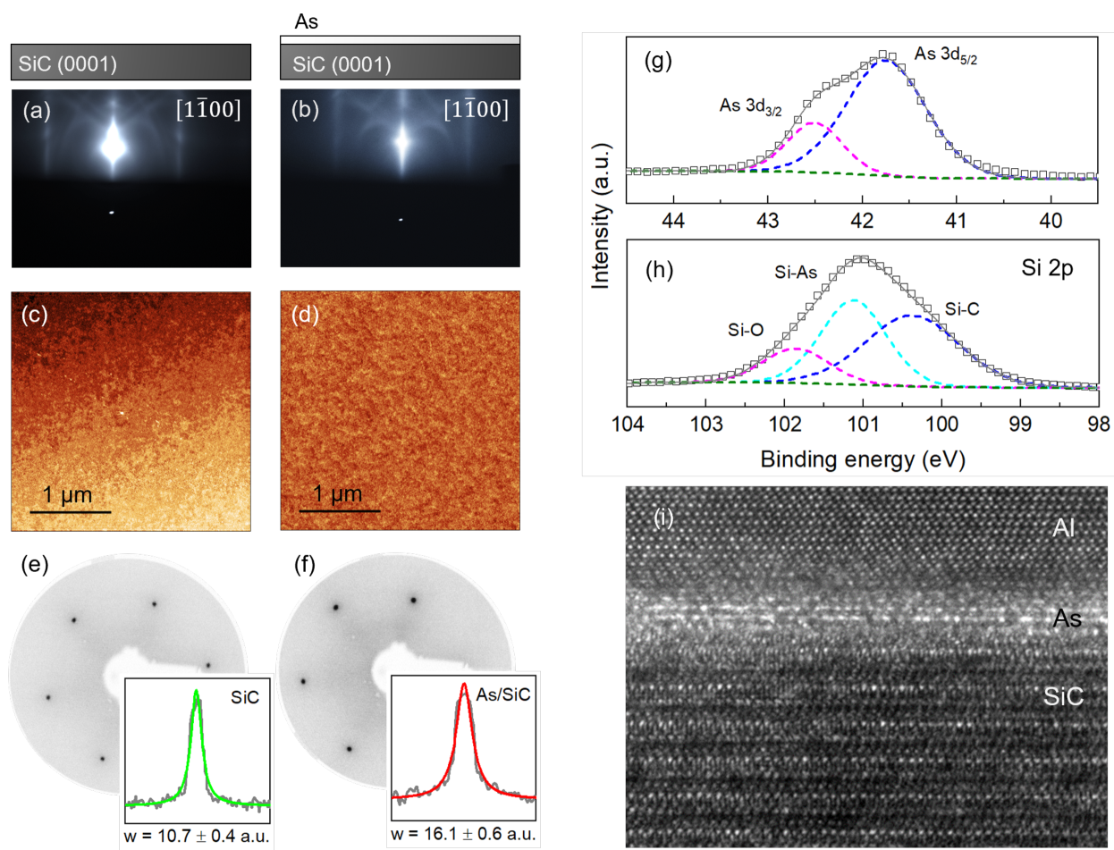
Figure 1(a) shows the RHEED pattern of bare SiC. The typical SiC surface step array is characterized by both the observed diffraction streaks and the splitting of the specular point. For substrate miscut angle lower than , the beam splitting can be seen at any azimuthal direction but parallel to the terrace edge [25]. In addition, Kikuchi lines from the SiC bulk are observed evidencing the high crystalline quality of the substrate. The presence of more than one specular spot due to the SiC terraces causes the central region in Fig. 1(a) to be broad and highly bright. After the As deposition, the central spot becomes thinner [Fig. 1(b)] indicating the vanishing of the SiC terraces. This result is corroborated by AFM images which exhibit clear terraces on the bare SiC [Fig. 1(c)] and a stepless homogeneous surface after As deposition [Fig. 1(d)]. The surface roughness of the deposited As shown in Fig. 1(d) was found nm rms over a scanned area. No significant differences in the RHEED streak distances were observed during and after the As deposition, suggesting a layer-by-layer growth mechanism for the deposited arsenene. To allow layer-by-layer growth, the As bond with substrate should be stronger than the As-As interaction [26], yielding arsenene to be formed on SiC. Indeed, our ab initio calculations confirm an exothermic process of As4 bonding to SiC surface. Free-standing planar arsenene has been predicted to not be dynamically stable [13; 27].
LEED patterns were also recorded prior to and after the As deposition. As shown in Fig. 1(e), sharp LEED spots in a low diffuse background were observed for bare SiC. This pattern, from the unreconstructed SiC after annealing at C, indicates a high-quality (smooth and well-organized) substrate surface. After the As deposition, no reconstruction was observed [Fig. 1(f)], corroborating that the arsenic layers grow with the same orientation of the SiC unit cell. The LEED spot profiles [inset in Fig. 1(e) and (f)] show a significant broadening of the diffraction peak from a.u. to a.u. for the full width at half maximum (w) when As is deposited. Such an increase can be related to the overlap of the diffraction spots of the SiC substrate and that of the grown arsenene, indicating a slight increase of the surface disorder upon the As deposition. Finally, from the distances between dots on the LEED pattern, we find that the lattice constant (a) of the deposited arsenene is Å. This value is very similar to that reported in the literature for bare hexagonal SiC ( Å) [28]. This result clearly indicates that the epitaxially deposited arsenene follows the very same surface structure of the SiC. Here it is worth noticing that arsenene is in contrast with the honeycomb reconstruction observed on SiC bismuthene, which can be understood by our ab initio results below. From the lattice mismatch between 6H-SiC nearest neighbor sites (d Å) and that of freestanding two-dimensional buckled arsenene (d Å) [13; 28] the induced tensile strain on the deposited arsenene can be estimated as .
Highly strained arsenene could be epitaxially grown thanks to the strong As interaction with SiC. In order to examine such an interaction, XPS analyses have been carried out. Fig. 1(g) and (h) show the respective high-resolution As 3d and Si 2p XPS spectra of the sample after etching at the XPS chamber. As 3d3/2 and As 3d5/2 peaks are observed at and eV, respectively [29]. The absence of a third peak at eV typically ascribed to oxidized As (e.g. As2O3) [30; 31; 32] demonstrate that the etching procedure efficiently removed the As oxide layer. Concerning the Si 2p XPS spectrum, the peaks identified correpond to SiC, SiAs and SiO, at eV, eV and eV[29], respectively [Fig. 1(h)]. The presence of SiO may refer to the remaning oxygen passivation layer onto SiC not completely removed during the hydrogen etching. The identification of the Si-As peak is evidence of the covalent bonding formation between SiC and arsenene. The covalent bonding between Si and As has been corroborated by DFT calculations, as discussed hereafter. Finally, the epitaxial growth of arsenene on SiC has also been probed by HRTEM cross-section imaging as shown in Fig. 1(i). The HRTEM image shows a few-layer arsenene sandwiched between the SiC substrate and the Al capping layer. From Fig. 1(i), however, no distinction between the common arsenene allotropes (viz. planar, buckled, and puckered) is possible. The uppermost interface of the arsenene layers is not sharp likely due to the energetic Al atoms deposited during the capping layer preparation. Additionally, the arsenene/SiC interface is subject to the substrate roughness.
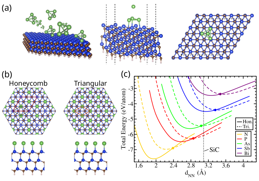
Despite flat antimonene and bismuthene experimental growth on SiC surfaces their flat As counterparts were grown and theoretically explored on metallic surfaces [33; 34]. Here, in our MBE experiments, a flux of As4 molecules is directed to the SiC substrate. Our ab-initio calculations indicate an energetically favorable binding energy of the As4 molecule on the SiC surface, with a binding energy of eV/As. In Fig. 2(a) we show the final configuration of As4 on the SiC surface, indicating a possible triangular structure, as the As binds to the nearest-neighbor Si surface lone-pairs. Our experimental electron diffraction results indicate that the presence of the As on the SiC surface does not lead to reconstruction, that is, the As layer follows the bare SiC surface periodicity. A different scenario is described in the literature for the Sb and Bi cases, where a honeycomb lattice reconstruction is observed [35; 36]. We have calculated the formation energy () of a honeycomb and a triangular phase of As on SiC [Fig. 2(b)]
| (1) |
where final/initial systems are the SiC slab with/without the arsenic first layer, is the total energy of an isolated As4 molecule, and the number of As per unit cell in the first layer. The triangular phase is energetically favored by eV/As, with and eV/As for honeycomb and triangular, respectively. Here we can understand the deviating behavior of As compared to Sb and Bi structures by comparing the energetics of a honeycomb lattice and a triangular lattice for the pnictogen family as a function of the interatomic distance. Notice here that in order to capture the substrate effect we have replaced the SiC slab with passivation of the bottom part of each layer with hydrogen, which is shown to correctly capture the pnictogen/SiC systems properties [37; 11]. In Fig. 2(c) the vertical dashed line marks the SiC surface lattice nearest-neighbor (NN) distance. For the Sb and Bi atoms, which present a larger atomic radius, the lower site density honeycomb lattice, is more stable on the SiC lattice parameter. However, for the lower atomic radius pnictogens, a lattice with a higher site density is more stable, stabilizing the triangular reconstruction. Interestingly such analysis is consistent with the observed honeycomb lattice of As on Cu, Ag, and Au (111) surfaces [33; 34], which presents dNN between and Å, that is, in the region where the honeycomb lattice is energetically favorable, Fig. 2(c).
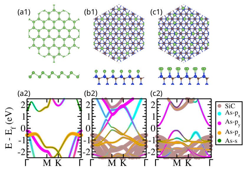
From the electronic perspective, the freestanding arsenene in its buckled structure [Fig. 3(a1)] is known for being a topologically trivial semiconductor, Fig. 3(a2). Previous studies have discussed that tensile strain over in arsenene a topological trivial non-trivial transition would be present [27]. However, as discussed the arsenene system goes through a structural phase transition [honeycomb triangular] in strain, Fig. 2(c). Here, the arsenene bands neatly lie within the SiC band gap, Fig. 3(b2) and (c2). The symmetric triangular structure presents a metallic phase with a vanish velocity band (high density of states) resonant with the Fermi energy along the dispersion, Fig. 3(b2). This electronic picture gives rise to a Peierls-like structural transition where a gap of eV is opened on the As-p states, Fig. 3(c2). Such Peierls-like trimerization presents an atomic distortion with average atomic dislocation of Å, and an energetic preference of eV/As [Fig. 3(c1)].
| interface | (eV/As) | (meV/As) |
|---|---|---|
| 1.99 | -32 | |
| 0.05 | -9 | |
| 0.36 | -20 | |
| 1.00 | -45 | |
| 0.36 | -22 | |
| -0.22 | -52 | |
| 0.06 | 0 | |
| 0.80 | -59 | |
| 0.78 | -59 | |
| 1.73 | 1 |
The experimental results are also suggesting that the system does not grow thicker arsenene slabs. We have explored the multilayer arsenene system supported by SiC. Note that the first arsenene layer is bonded covalently with the SiC substrate in a triangular structure with exfoliation energy of meV/Å2. In order to understand the energetically stable second layer we have explored different cell mismatches both in a Triangular/Triangular interface as well as a Triangular/Hexagonal interface, which we summarize in Table 1, where the first Triangular layer is constrained with the SiC lattice periodicity. We have found that a second layer hexagonal cell [] matched with an triangular cell [] interface, namely , is the most stable system explored. We can understand such preference arising both from the lower strain in the second layer [], as well as an increased interaction energy meV/As. The interaction energy is inferred from the second layer formation energy, ruled by interaction plus strain energy, , being the interaction energy always negative, attractive vdW coupling, while the strain energy is always positive. Although in the smaller commensurable system and a stronger binding energy is achieved, the lower strain presented on the dictates the favorable formation energy. From the results, we can understand that a perfectly decoupled second layer is the more stable configuration.
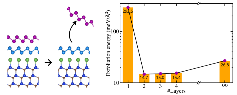
The decoupled character of the second layer present a binding energy ruled by vdW interaction giving a exfoliation energy of only meV/Å2. Such scale of values is maintained for 3 and 4 stacked layers, with the exfoliation energy of the top-most layer being, for instance, lower than that calculated for graphene meV/Å2. In contrast, the gray arsenic bulk presents a exfoliation energy of meV/Å2 [Fig. 4]. Here we can expect that, despite gray arsenic being stable, few layers arsenene presents a lower interlayer interaction leading to a possible self limited growth.
IV Conclusions
In summary, we reported the experimental synthesis of 2D arsenene supported by SiC. Our electron diffraction results predict a new triangular arsenene allotrope which was confirmed by our ab initio calculations. The strain field arising in the arsenene first layer over silicon carbide drives a structure transition from the honeycomb freestanding system to the supported triangular. The silicon carbide, beyond serving as a generator of the strain field, with its insulating electronic character allows for the relevant arsenene state to neatly lie within its energy gap. Such a new triangular allotrope, present a Peierls-like distortion, leading to an indirect semiconducting character with a eV. Our ab initio results also indicate a possible self-limited epitaxial growth of a few layers arsenene given its decoupling of the second non-covalent layer.
Acknowledgements.
The authors acknowledge financial support from the São Paulo Research Foundation FAPESP (Grant numbers 21/06238-5, 19/14949-9, 19/20857-0, and 17/02317-2), INCT-Nanocarbono, INCT-Materials Informatics, and Laboratório Nacional de Computação Científica for computer time (project ScafMat2). R.F.O. acknowledges additional support from INCT/INEO.References
- Ahn et al. [2017] G. H. Ahn, M. Amani, H. Rasool, D.-H. ien, J. P. Mastandrea, J. W. Ager III, M. Dubey, D. C. Chrzan, A. M. Minor, and A. Javey, “Strain-engineered growth of two-dimensional materials,” Nature Communications 8, 608 (2017).
- Dai, Liu, and Zhang [2019] Z. Dai, L. Liu, and Z. Zhang, “Strain Engineering of 2D Materials: Issues and Opportunities at the Interface,” Advanced Materials 31, 1805417 (2019).
- Kim et al. [2022] J. M. Kim, M. F. Haque, E. Y. Hsieh, S. M. Nahid, I. Zarin, K.-Y. Jeong, J.-P. So, H.-G. Park, and S. Nam, “Strain Engineering of Low-Dimensional Materials for Emerging Quantum Phenomena and Functionalities,” Advanced Materials , 2107362 (2022).
- Conley et al. [2013] H. J. Conley, B. Wang, J. I. Ziegler, R. F. J. Haglund, S. T. Pantelides, and K. I. Bolotin, “Bandgap Engineering of Strained Monolayer and Bilayer MoS2,” Nano Letters 13, 3626–3630 (2013).
- Chowdhury et al. [2021] T. Chowdhury, K. Jo, S. B. Anantharaman, T. H. Brintlinger, D. Jariwala, and T. J. Kempa, “Anomalous Room-Temperature Photoluminescence from Nanostrained MoSe2 Monolayers,” ACS Photonics 8, 2220–2226 (2021).
- Lin et al. [2022] C. Lin, L. Cai, J.-H. Fu, S. Sattar, Q. Wang, Y. Wan, C.-C. Tseng, C.-W. Yang, A. Aljarb, K. Jiang, K.-W. Huang, L.-J. Li, C. M. Canali, Y. Shi, and V. Tung, “Direct Band Gap in Multilayer Transition Metal Dichalcogenide Nanoscrolls with Enhanced Photoluminescence,” ACS Materials Letters 4, 1547–1555 (2022).
- Peng et al. [2020] Z. Peng, X. Chen, Y. Fan, D. J. Srolovitz, and D. Lei, “Strain engineering of 2D semiconductors and graphene: from strain fields to band-structure tuning and photonic applications,” Light: Science & Applications 9, 190 (2020).
- Guinea, Katsnelson, and Geim [2010] F. Guinea, M. I. Katsnelson, and A. K. Geim, “Energy gaps and a zero-field quantum Hall effect in graphene by strain engineering,” Nature Physics 6, 30–33 (2010).
- Hu et al. [2022] Y. Hu, J. Liang, Y. Xia, C. Zhao, M. Jiang, J. Ma, Z. Tie, and Z. Jin, “2D Arsenene and Arsenic Materials: Fundamental Properties, Preparation, and Applications,” Small 18, 2104556 (2022).
- Zhang et al. [2018] S. Zhang, S. Guo, Z. Chen, Y. Wang, H. Gao, J. Gómez-Herrero, P. Ares, F. Zamora, Z. Zhu, and H. Zeng, “Recent progress in 2D group-VA semiconductors: from theory to experiment,” Chem. Soc. Rev. 47, 982–1021 (2018).
- Costa et al. [2019] M. Costa, G. R. Schleder, M. Buongiorno Nardelli, C. Lewenkopf, and A. Fazzio, “Toward Realistic Amorphous Topological Insulators,” Nano Letters 19, 8941–8946 (2019).
- Focassio et al. [2021] B. Focassio, G. R. Schleder, M. Costa, A. Fazzio, and C. Lewenkopf, “Structural and electronic properties of realistic two-dimensional amorphous topological insulators,” 2D Materials 8, 025032 (2021).
- Kamal and Ezawa [2015] C. Kamal and M. Ezawa, “Arsenene: Two-dimensional buckled and puckered honeycomb arsenic systems,” Phys. Rev. B 91, 085423 (2015).
- Wang et al. [2016] C. Wang, Q. Xia, Y. Nie, M. Rahman, and G. Guo, “Strain engineering band gap, effective mass and anisotropic Dirac-like cone in monolayer arsenene,” AIP Advances 6, 035204 (2016).
- Zhang, Ma, and Chen [2015] H. Zhang, Y. Ma, and Z. Chen, “Quantum spin hall insulators in strain-modified arsenene,” Nanoscale 7, 19152–19159 (2015).
- [16] A. Pal, S. Zhang, T. Chavan, K. Agashiwala, C.-H. Yeh, W. Cao, and K. Banerjee, “Quantum-Engineered Devices Based on 2D Materials for Next-Generation Information Processing and Storage,” Advanced Materials , 2109894.
- Roldán et al. [2015] R. Roldán, A. Castellanos-Gomez, E. Cappelluti, and F. Guinea, “Strain engineering in semiconducting two-dimensional crystals,” Journal of Physics: Condensed Matter 27, 313201 (2015).
- Matsunami [2004] H. Matsunami, “Technological Breakthroughs in Growth Control of Silicon Carbide for High Power Electronic Devices,” Japanese Journal of Applied Physics 43, 6835 (2004).
- Xu et al. [2018] W.-W. Xu, F. Xia, L. Chen, M. Wu, T. Gang, and Y. Huang, “High-temperature mechanical and thermodynamic properties of silicon carbide polytypes,” Journal of Alloys and Compounds 768, 722–732 (2018).
- Kresse and Hafner [1993] G. Kresse and J. Hafner, “Ab initio molecular dynamics for open-shell transition metals,” Phys. Rev. B 48, 13115–13118 (1993).
- Kresse and Furthmüller [1996] G. Kresse and J. Furthmüller, “Efficient iterative schemes for ab initio total-energy calculations using a plane-wave basis set,” Phys. Rev. B 54, 11169–11186 (1996).
- Perdew, Burke, and Ernzerhof [1996] J. P. Perdew, K. Burke, and M. Ernzerhof, “Generalized Gradient Approximation Made Simple,” Phys. Rev. Lett. 77, 3865–3868 (1996).
- Dion et al. [2004] M. Dion, H. Rydberg, E. Schröder, D. C. Langreth, and B. I. Lundqvist, “Van der Waals Density Functional for General Geometries,” Phys. Rev. Lett. 92, 246401 (2004).
- Padilha et al. [2019] J. Padilha, R. Pontes, F. C. de Lima, R. Kagimura, and R. Miwa, “Graphene on the oxidized SiC surface and the impact of the metal intercalation,” Carbon 145, 603–613 (2019).
- hong Zhu, Brunner, and Abstreiter [1999] J. hong Zhu, K. Brunner, and G. Abstreiter, “Step characterization on vicinal Si surfaces by reflection high-energy electron diffraction at arbitrary azimuths,” Applied Surface Science 137, 191–196 (1999).
- Lozovoy et al. [2020] K. A. Lozovoy, A. G. Korotaev, A. P. Kokhanenko, V. V. Dirko, and A. V. Voitsekhovskii, “Kinetics of epitaxial formation of nanostructures by Frank–van der Merwe, Volmer–Weber and Stranski–Krastanow growth modes,” Surface and Coatings Technology 384, 125289 (2020).
- Rahman, Mahmood, and García-Suárez [2019] G. Rahman, A. Mahmood, and V. M. García-Suárez, “Dynamically stable topological phase of arsenene,” Scientific Reports 9, 7966 (2019).
- Jones [2008] K. Jones, “Structural analyses for sic and algan grown on off-axis 4h- and 6h-sic,” Journal of Crystal Growth 310, 2417–2426 (2008).
- Rochet et al. [1995] F. Rochet, C. Poncey, G. Dufour, H. Roulet, W. Rodrigues, M. Sauvage, J. Boulliard, F. Sirotti, and G. Panaccione, “The As-terminated Si(001) surface and its oxidation in molecular oxygen: an Si 2p and As 3d core-level study with synchrotron radiation,” Surface Science 326, 229–242 (1995).
- Chen et al. [2021] C. Chen, C. Li, Q. Yu, X. Shi, Y. Zhang, J. Chen, K. Liu, Y. He, and K. Zhang, “Bandgap opening in layered gray arsenic alloy,” APL Materials 9, 041102 (2021).
- Antonatos et al. [2020] N. Antonatos, V. Mazánek, P. Lazar, J. Sturala, and Z. Sofer, “Acetonitrile-assisted exfoliation of layered grey and black arsenic: contrasting properties,” Nanoscale Adv. 2, 1282–1289 (2020).
- [32] “NIST X-ray Photoelectron Spectroscopy Database,” .
- Shah et al. [2020] J. Shah, W. Wang, H. M. Sohail, and R. I. G. Uhrberg, “Experimental evidence of monolayer arsenene: an exotic 2D semiconducting material,” 2D Materials 7, 025013 (2020).
- Kang, Noh, and Han [2019] J. Kang, S. H. Noh, and B. Han, “First-principles computational design of unknown flat arsenene epitaxially grown on copper substrate,” Applied Surface Science 467-468, 561–566 (2019).
- Reis et al. [2017] F. Reis, G. Li, L. Dudy, M. Bauernfeind, S. Glass, W. Hanke, R. Thomale, J. Schafer, and R. Claessen, “Bismuthene on a SiC substrate: A candidate for a high-temperature quantum spin Hall material,” Science 357, 287–290 (2017).
- Shao et al. [2018] Y. Shao, Z.-L. Liu, C. Cheng, X. Wu, H. Liu, C. Liu, J.-O. Wang, S.-Y. Zhu, Y.-Q. Wang, D.-X. Shi, K. Ibrahim, J.-T. Sun, Y.-L. Wang, and H.-J. Gao, “Epitaxial Growth of Flat Antimonene Monolayer: A New Honeycomb Analogue of Graphene,” Nano Letters 18, 2133–2139 (2018).
- Hsu et al. [2015] C.-H. Hsu, Z.-Q. Huang, F.-C. Chuang, C.-C. Kuo, Y.-T. Liu, H. Lin, and A. Bansil, “The nontrivial electronic structure of Bi/Sb honeycombs on SiC(0001),” New Journal of Physics 17, 025005 (2015).