The NectarCAM Timing System
Abstract
NectarCAM is a Cherenkov camera which is going to equip the Medium-Sized Telescopes (MST) of the northern site of the Cherenkov Telescope Array Observatory (CTAO). NectarCAM is equipped with 265 modules, each consisting of 7 photo-multiplier tubes (PMTs), a Front-End Board and a local camera trigger system used for data acquisition. This paper addresses the timing performance of NectarCAM which are crucial to reduce the noise in shower images and improve image cleaning as well as to discriminate between gamma-ray photons and cosmic-ray background and finally to allow coincidence identification with neighbouring telescopes for stereoscopic operations. Verification tests of the system have been performed in a dark room using various light sources to illuminate the first NectarCAM unit. The resulting timing precision and accuracy of the trigger arrival relative to a laser source, of individual and multiple pixel signals have been studied and are shown to comply to CTAO requirements.
keywords:
NectarCAM , gamma ray , Cherenkov , CTAO , timing resolution , PMT transit time , trigger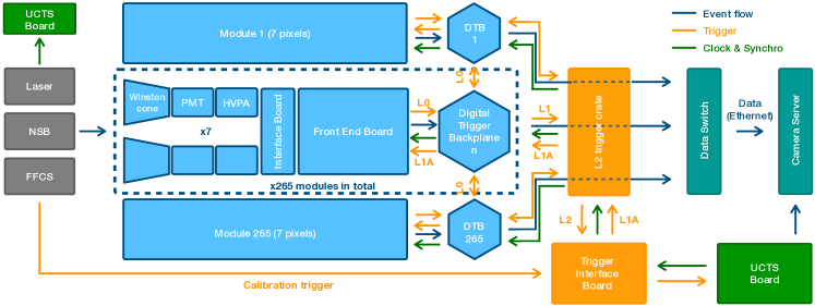
1 Introduction
The imaging atmospheric Cherenkov technique is one of the major methods for observations of very-high energy gamma rays on Earth, the other being the water Cherenkov technique [1, 2]. In the imaging atmospheric Cherenkov technique, gamma rays are detected indirectly via the Cherenkov light produced in particle cascades (showers) generated when they interact in the atmosphere. Images of the shower in one or several telescopes are analyzed to provide cosmic-ray background suppression and to reconstruct primary gamma-ray parameters.
CTAO is the major future facility in the field of astroparticle physics and high-energy astrophysics exploiting the imaging atmospheric Cherenkov technique [3]. The CTA Observatory will explore the high-energy universe with gamma rays between 20 GeV and 300 TeV [4]. It consists of several tens of telescopes distributed over two sites, in La Palma (Spain) and in Paranal (Chile), in three different sizes: Small-Sized Telescope (SST), Medium-Sized Telescope (MST) and Large-Sized Telescope (LST). The telescopes consist of tessellated mirrors which focus the Cherenkov photons arriving within a few nanoseconds onto fast-recording, pixelated cameras. In order to properly combine the spatial and temporal information of these short light pulses from all the telescope cameras and accurately reconstruct the properties of the observed air shower, precise knowledge of the shower image timing is mandatory.
In this paper, we present the timing performance of NectarCAM, the camera designed to equip the MST telescopes at the CTA-North site [5]. The Cherenkov signal arrives in individual pixels in a time interval of 2–4 ns. The relative timing of individual pixels can be used to reduce the night sky background for low-energy gamma-ray showers, which give signals in just a few pixels in the camera. On the other hand, high-energy showers can give images with a time gradient in the camera that can last up to several tens of ns. The relative timing information between pixels can be used to calculate the shower time gradient. Finally, stereoscopy allows to reduce the camera trigger and acquisition rate by rejecting events that are not seen by several telescopes. For this, the relative time between telescopes must be known with an accuracy of tens of ns, but in addition the geometry of the Cherenkov wavefront can be measured if an accuracy of a few ns is achieved. Therefore, there are three types of timing uncertainty that need to be characterized: the single pixel precision, limited by the quantization noise of the chip responsible for the signal read-out; the total camera timing precision, which takes into account the timing difference between each pair of pixels, and the timing accuracy associated to the camera trigger timestamp. Each of these timing uncertainties has been quantified with the first NectarCAM camera unit in the darkroom at the integration and test facility at CEA (Commissariat à l’Énergie Atomique et aux Énergies Alternatives) Paris-Saclay. These tests are also required by CTAO since it follows a verification-based product acceptance procedure, according to which all products must fulfill a list of performance requirements before their deployment on site.
In the following, the timing accuracy and systematic uncertainties are presented for both single pixels and the full camera together with the overall performance of the camera trigger.
2 NectarCAM
NectarCAM has a modular design, with a basic element (“module”) consisting of a focal plane module (FPM) and a front-end board (FEB). The FPM [6] is composed of seven 1.5” R12992-100-05 Hamamatsu photomultiplier tubes (PMTs) associated with high voltage and pre-amplification boards (HVPA) sitting in the FEB, and equipped with Winston cone light concentrators [7].
2.1 Camera readout
Cherenkov light impinging on the camera is converted into an electrical signal by the PMTs and preamplified into two (high and low gain) signals. The Amplifier for CTA (ACTA) [8] application specific integrated circuit (ASIC) chip of the FEB amplifies again the high gain signal and splits the output into the high gain signal input to the NECTAr chip [9] and the trigger level 0 (L0), while the low gain signal is simply amplified to enter another channel of the NECTAr chip. The latter comprises a switched capacitor array which samples the signal at 1 GHz , and a 12-bit analogue-to-digital converter (ADC), responsible for the digitization of each sample once the trigger signal is received. The NECTAr chip acts as a circular buffer which holds 1 microsecond of data until a camera trigger occurs. The camera is triggered in a multistep process (see the following section for details). When the trigger conditions are met, the photon signal is digitized, and the full waveform for every pixel sent to a camera server through an ethernet-based data acquisition system. The camera server is a remote machine located outside the camera frame, in the CTAO on-site data center farm running the NectarCAM acquisition software. The data are transferred via 10 Gbps optical fibres. An absolute time-stamp is also assigned to the trigger signal (see 2.3 below), so that images from multiple telescopes can be later combined.
2.2 Camera trigger
NectarCAM is triggered when it receives a significant amount of light in a compact region of the detection plane within a short period of time (typically a few ns) [10]. Translated in terms of camera hardware, this means that several neighboring pixels will see photon signals within a few nanoseconds. A schematic of the hardware architecture of the digital trigger of NectarCAM is shown in Figure 1\xspace.
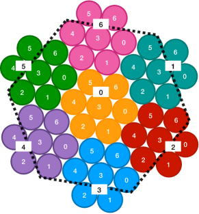
The first trigger level (level 0 trigger or L0) [11] occurs in each FEB in an ASIC: it processes the analogue signals coming from the seven individual PMTs in each module, by comparing each pixel amplitude with a threshold value. If the signal in a pixel exceeds the settable threshold, a digital L0 signal is produced for that pixel. The L0 digital signal is then sent to an FPGA located on the digital trigger backplane (DTB) of that module, where the level 1 (L1) trigger signal is formed by processing the L0 signals of that module and signals from the nearest 5 of the 7 PMTs in the 6 neighboring modules, forming a 37-pixel region, as indicated by the area contained within the dashed black line in Figure 2\xspace. Each module’s DTB uses the 3 nearest neighbours (3NN) algorithm [10] implemented in its FPGA to form a L1 trigger signal out of the 37 L0 signals. The 3NN algorithm was tested with simulations and real data [12].
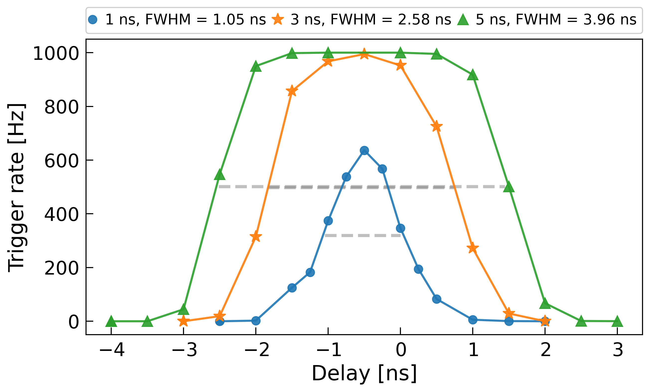
The FPGA distributes the L0 signals of a module to its six neighbours and in parallel receives their L0 outputs (see Figure 2\xspace). The delay of each of the 37 L0 signals can be adjusted digitally in steps of 50 ps, before entering the trigger chain. The 3NN trigger algorithm generates a trigger, if within the 37 pixel area 3 adjacent pixels within a 3 ns discrete time window are above a discrimination threshold. The time window width of 3 ns is the default value on the first NectarCAM. This is justified by the study illustrated in Figure 3\xspace, which shows the rate of occurring L1 triggers within three different time windows. The delay on the horizontal axis has been obtained by directly injecting light into three connected pixels (either oriented inline or triangular) belonging to three neighboring modules with optical fibers. The optical fibers produce a short duration pulse approximately 5 ns wide (full-width half-maximum, FWHM), with around 3 ns rise time (from 10% to 90% of full amplitude) [13]. The delay of one fiber with respect to the others has been changed and three different values of time window (1 ns, 3 ns and 5 ns) have been tried. As can be seen in Figure 3\xspace, the 1 ns time-window misses more than 40% of the triggers. The 3 ns time-window is more than 95% efficient in the interval -1 ns to 0 ns and integrates less noise than the 5 ns time-window.
The L1 signals of each DTB (265 in total) are delivered to an L2-crate (L2C) where they are combined in an OR operation to generate the L2 trigger, i.e., the camera trigger, which is then sent to the trigger interface board (TIB) [14]. Depending on the configuration parameters and camera status, the TIB ignores the L2 or delivers it back as a L1 accepted (L1A) signal all the way back to the FEBs. At this point, the 1 GHz sampling of the NECTAr chips is stopped, the full 60 ns waveform for every pixel is digitized and transferred over ethernet to a camera server where the different components of the camera event are combined in an Event Builder process. In addition, the TIB delivers the camera trigger signal and the corresponding trigger-class bit associated to a type of event (e.g. pedestal, calibration, internal) to the Unified Clock distribution and Trigger time-Stamping (UCTS) module, where the event is time-stamped, as described below.
2.3 Camera absolute time-stamping system
The UCTS module contains primarily a timing and clock stamping (TiCkS) board [16], a node of a White Rabbit timing system [17], in order to provide an absolute time-stamp for the camera triggers. The White Rabbit system, developed initially at CERN, is an “Open Hardware” development for sub-nanosecond accuracy time-transfer, along with data transfer, by extending Synchronous ethernet with PTP (Precision Time Protocol) [18]. The TiCkS board is connected to a commercial White Rabbit Ethernet switch by a dedicated fibre, which is used for data and timing signal transmission in both directions at different wavelengths. The White Rabbit Switch receives absolute time from NTP (Network Time Protocol) combined with GPS time (Global Positioning System), and this time is transported to the White Rabbit nodes’ internal clocks.
The TiCkS internal clock is therefore continually kept at this distributed absolute time to within the CTA requirement of RMS relative to other CTA telescopes, thanks to the White Rabbit protocol. When it receives camera trigger signals from the TIB, over two low-voltage differential signalling pairs – for read-out or busy events222An event is flagged as busy when the TIB cannot send triggers to the FEBs because they are digitizing an event., respectively – it increments the respective event counter and stores the absolute time-stamp of that camera trigger, along with the trigger-class and other additional information on the event provided by the TIB over an SPI link (Serial Peripheral Interface) 333https://onlinedocs.microchip.com/pr/GUID-835917AF-E521-4046-AD59-DCB458EB8466-en-US-1/index.html?GUID-E4682943-46B9-4A20-A62C-33E8FD3343A3. The resulting trigger, counter, and camera information is sent in bunches as UDP (user datagram protocol)444https://www.rfc-editor.org/rfc/rfc768.txt packets over the White Rabbit fibre, and which are then combined with the camera pixel data based on the common event counters. This is carried out in the camera event builder process running on the camera server.
Also contained in the UCTS module is a Raspberry-Pi555https://www.raspberrypi.org based “Remote Programming Board” whose only function is to allow the firmware update of the TiCkS board over a JTAG link (Joint Test Action Group) [19], by connecting through the standard Camera ethernet switches to the Raspberry-pi processor, without the need to physically access the UCTS module.
3 Camera test setup
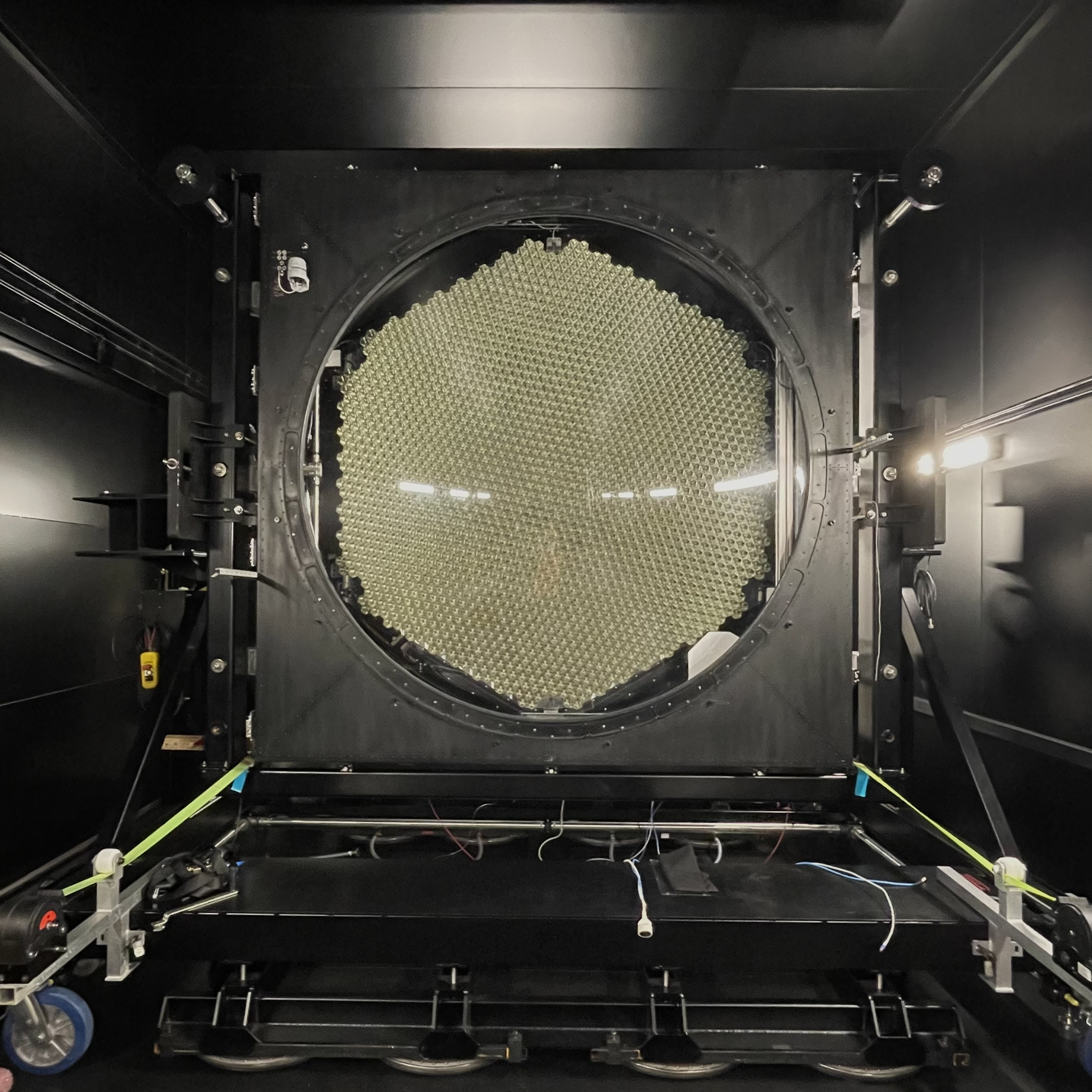
The first NectarCAM unit has been integrated at the integration and test facility of CEA Paris-Saclay. The test facility housing the camera consists of a m long temperature controlled dark room equipped with all camera services and calibration light sources, connected to a control room in which the full data acquisition (DAQ), storage and run control systems are located. The camera is equipped with the complete readout electronics consisting of 265 modules (1855 pixels), and with an entrance window, as can be seen in Figure 4\xspace. The readout data are sent by UDP to a dedicated camera server [20] through four pairs of 10 Gb/s optical links. A fifth optical fiber pair is used to control all camera devices from the control room using a graphical user interface running on a separate camera slow control server.
Three light sources are used to evaluate the camera at realistic intensities between roughly 1 and 12000 photons per pixel, corresponding to 0.25 and 3000 photoelectrons (p.e.) after conversion in the PMTs (using 25% collection efficiency). The charge versus number of photoelectrons measurement is linear to a very good approximation [21]. The three light sources are a flat field calibration pulsed light source (FFCLS), a continuous night sky background (NSB) emulating light, and a pulsed laser source. The FFCLS and the NSB sources are also controlled from the graphical interface in the control room. Once the camera is on-site, the FFCLS and the NSB sources are going to be used for calibration. However, a laser source is also used in the dark room to perform precise timing measurements.
The FFCLS consists of 13 light emitting diodes (LEDs), emitting pulsed light at 390 nm wavelength (FWHM of 3.3 ns) to reproduce the maximum of the received UV Cherenkov spectrum. A holographic filter is mounted in front of the LEDs in order to obtain a diffuse and uniform light emission on the camera. The intensity of the FFCLS can also be adjusted using transmission filters. An optical fiber connects the FFCLS directly to the TIB of the camera to give the possibility to trigger externally. Moreover, the flat-field calibration source can be triggered in internal mode periodically or by an external random generator. The random generator is made with a stable light source and a H12386 Hamamatsu photon counting head device666https://www.hamamatsu.com/content/dam/hamamatsu-photonics/sites/documents/99_SALES_LIBRARY/etd/H12386_TPMO1073E.pdf, which consists of a photomultiplier tube, a high-speed photon counting circuit, and a high-voltage power supply circuit. The photon counting output provides a random arrival time which is used for the generation of a random trigger. The uniformity of the FFCLS light emission across the camera has been measured to be better than 2%.
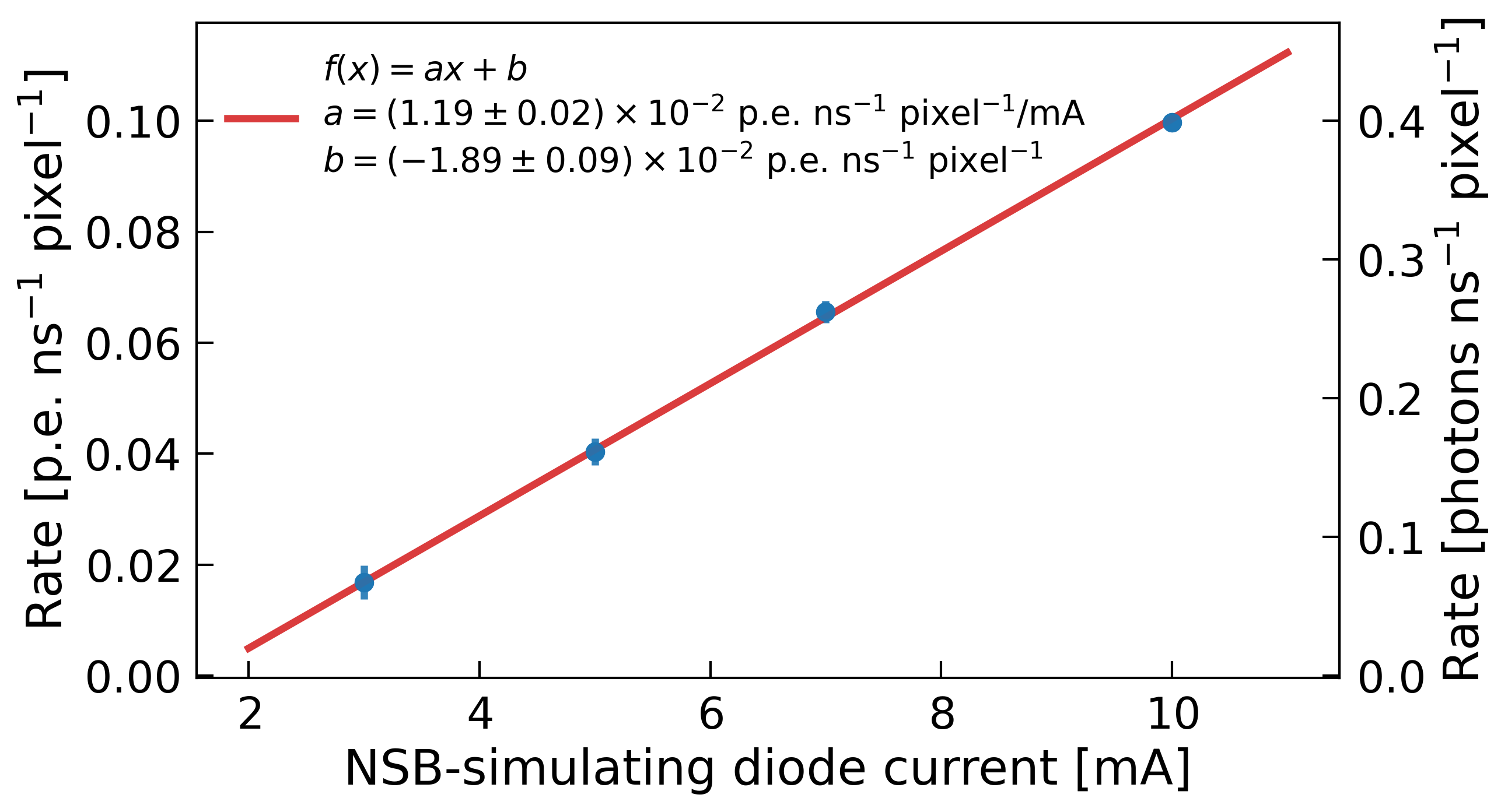
The NSB light source is used in order to reproduce the median photoelectron rate of the typical night sky spectrum. The light is created by a 519 nm LED in combination with a tunable diaphragm, resulting in a light output with spatial uniformity at the camera level better than 5% RMS. The NSB source has been calibrated by illuminating the camera with a low energy flux and counting the number of photons in the full 60 ns waveform length for each camera pixel. The result of the calibration is shown in Figure 5\xspace, where the number of photoelectrons measured per nanosecond and pixel is plotted as a function of the NSB current.
The laser source is a pulsed diode (Picoquant LDH-IB-375-B777https://www.picoquant.com/images/uploads/downloads/18451-ldh-i_series.pdf, ps width) creating a uniform illumination of the full camera at a wavelength of 373 nm. The light from the laser is attenuated and sent to the camera through a diaphragm. The total attenuation was measured to be 38. The laser is also connected to a UCTS board that records the timestamp of the photon laser pulse through a TiCkS board, allowing to perform precise measurements of the camera timing performance. According to the manufacturer, the jitter of the laser is ps (FWHM), therefore it is going to be considered negligibly small in the rest of the paper.
All light sources are at a distance of 12 m from the center of NectarCAM.
4 Time of Maximum
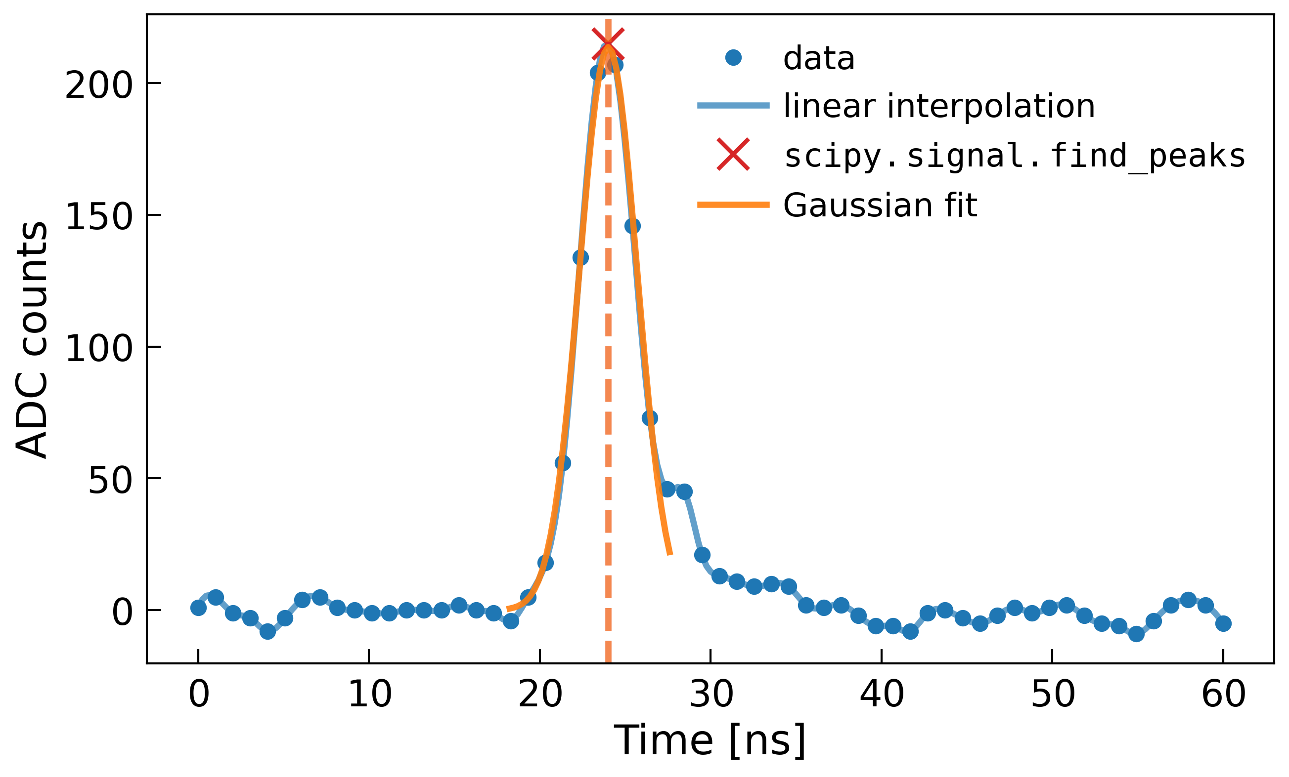
The temporal information of a PMT signal is sampled every nanosecond for a total window of 60 ns. The reconstructed arrival time of the pulse signal is given by the temporal position of the pulse maximum in the sampled window. This variable is called time of maximum (TOM).
The TOM is estimated from the waveform after subtracting the pedestal. Two methods have been used (see Figure 6\xspace). The first consists in identifying the position of the largest peak of the waveform using the function signal.find_peaks from the scipy python package [22]. The result was then cross-checked by performing a Gaussian fit of the largest peak of the waveform using as initialization value the position of the peak obtained from the first method.
5 Single pixel timing precision
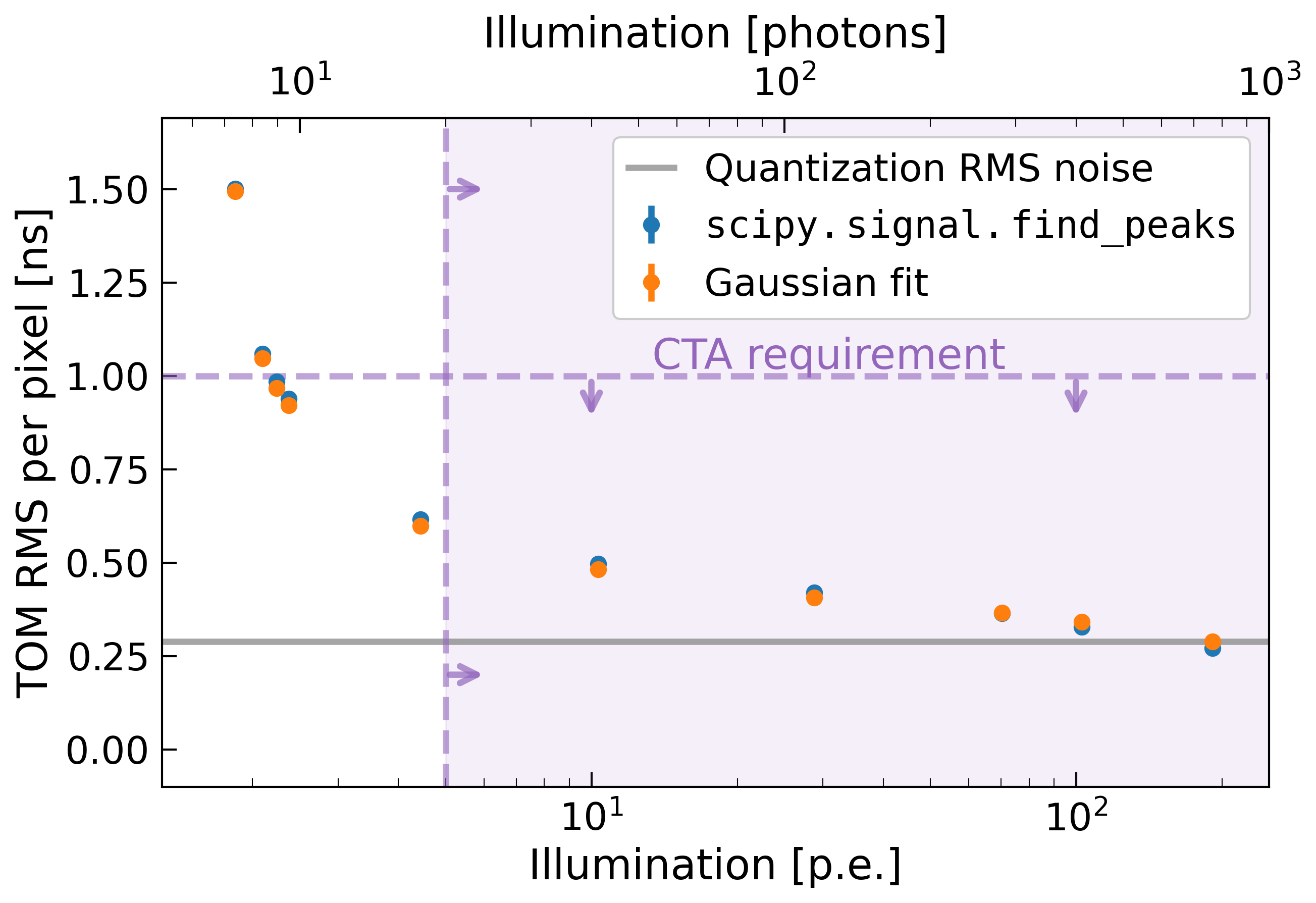
According to CTA requirements, NectarCAM needs to have a single pixel timing precision better than 1 ns for a light illumination larger than 20 photons (i.e., 5 p.e.). To estimate the single pixel timing precision, we illuminate the camera with a uniform light created by the laser source at a frequency of 1 kHz with pulsed energies between 8 pJ and 20 pJ, and we measure the TOM of each pulse for each pixel. Laser energies per pulse of 8 pJ and 20 pJ correspond to expected numbers of photons of p.e. and p.e. per pixel, respectively. The 2.5-fold difference in laser power displayed on the laser driver corresponds to a 200-fold difference in photoelectrons measured in the camera due to the non-linearity of the laser output. The TOM of individual events has been calculated using both methods described in Section 4\xspace and are in agreement within 50 ps. As explained later, the dispersion of the TOM of events for a given pixel gets a contribution from the random starting time of the NECTAr chip readout. The systematic timing uncertainty of each pixel can be estimated by the root mean square (RMS) of the obtained TOM distributions. Figure 7\xspace shows the weighted mean of the RMS over all the pixels as a function of the illumination charge. The results from both methods are shown. The weight is given by the inverse of the square of the standard deviation of the TOM distribution of each pixel. For an incoming light of intensity above photons, both methods show that the time precision is better than 1 ns, fulfilling the CTA requirement according to which the RMS uncertainty on the mean relative reconstructed arrival time in every pixel must not exceed 1 ns for amplitudes in the range 20 to 2000 photons (see violet dashed line and area). However, already at a light illumination of 800 photons, the pixel time precision limit is reached, as shown by the gray dashed line. This limit is due to the quantization of the L1A trigger acceptance signal by the NECTAr chip. This is due to the asynchronous arrival of the LA1 trigger with respect to the NECTAr chip clock. Since the NECTAr chip samples at 1 GHz, this corresponds to an RMS of ps.
6 PMT transit time
Prior to the estimation of the camera global timing precision, it is necessary to perform a relative calibration of the TOM over all the 1855 pixels. Two systematic effects combine to generate offsets. The first one is caused by the different arrival times of a L1A trigger signal from the TIB to the modules due to a different jitter in the FPGA of each DTB [23]. The L1A signal is sent by the TIB to the front end modules to stop the GHz sampling of the NECTAr chips and start acquiring the waveform data. The time dispersion due to L1A delay between modules can be corrected by tuning a delay in each digital backplane. The method is similar to the more complex PMT transit time calibration, which will be described in this paragraph, except that the former can be corrected during data taking while the latter can only be corrected at the analysis stage.
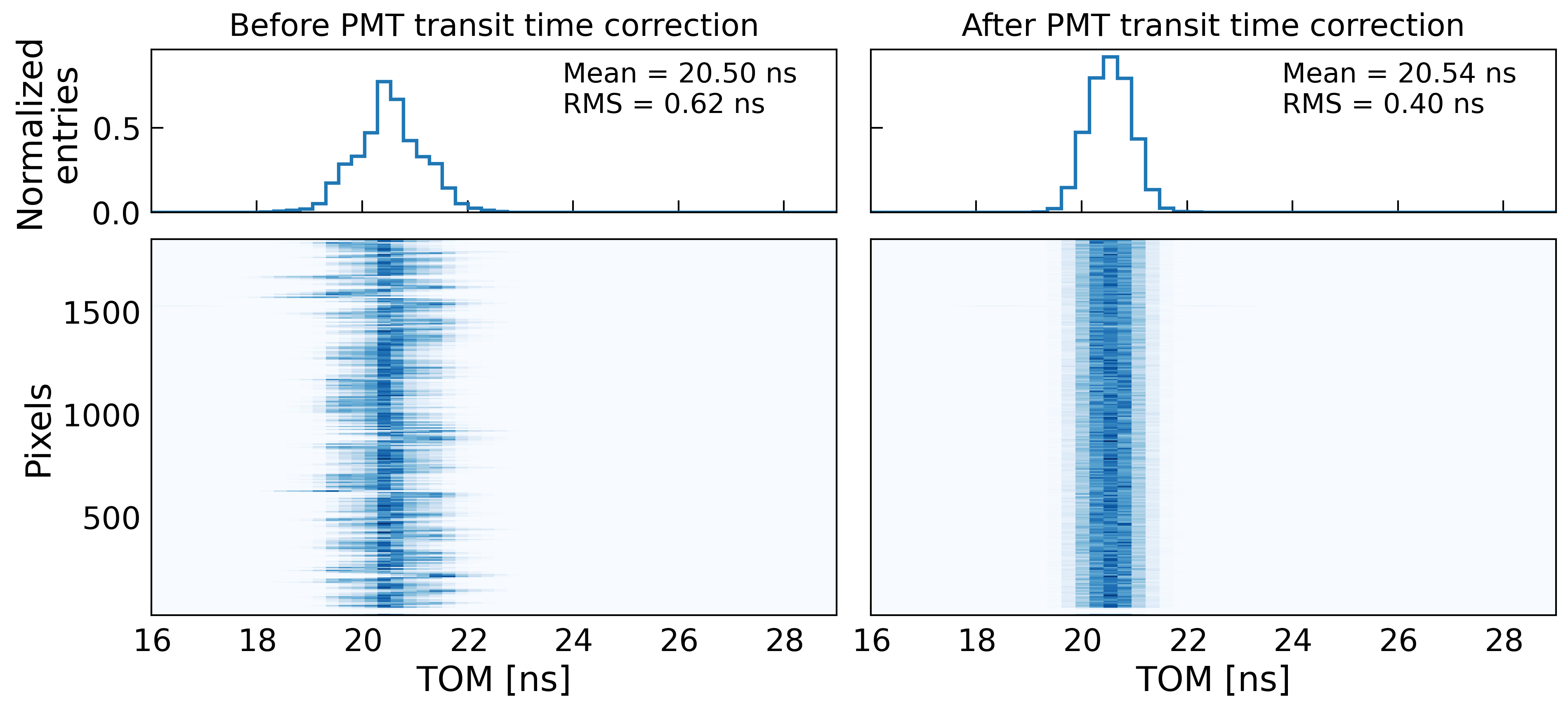
The second effect is the PMT transit time, which is the transfer time of the electron avalanche in the PMT [24] and depends on the high voltage applied to the dynodes. However, the high voltages also determine the amplitude of the output pulses of the PMTs. Therefore, since they are selected for each pixel in order to have the same nominal gain of 40000 over all the camera detection plane, the PMTs will introduce different delays, typically degrading the trigger performance. The drop in telescope performance in terms of effective area due to the PMT transit time becomes especially noticeable for gamma-ray energies smaller than 100 GeV [25]. However, this time offset between pixels can be corrected at the analysis level in order to improve the time resolution of the camera. The effect of the transit time spread between pixels is illustrated by the left panel of Figure 8\xspace, showing that the mean TOM distributions for all pixels do not overlap but are shifted in time.
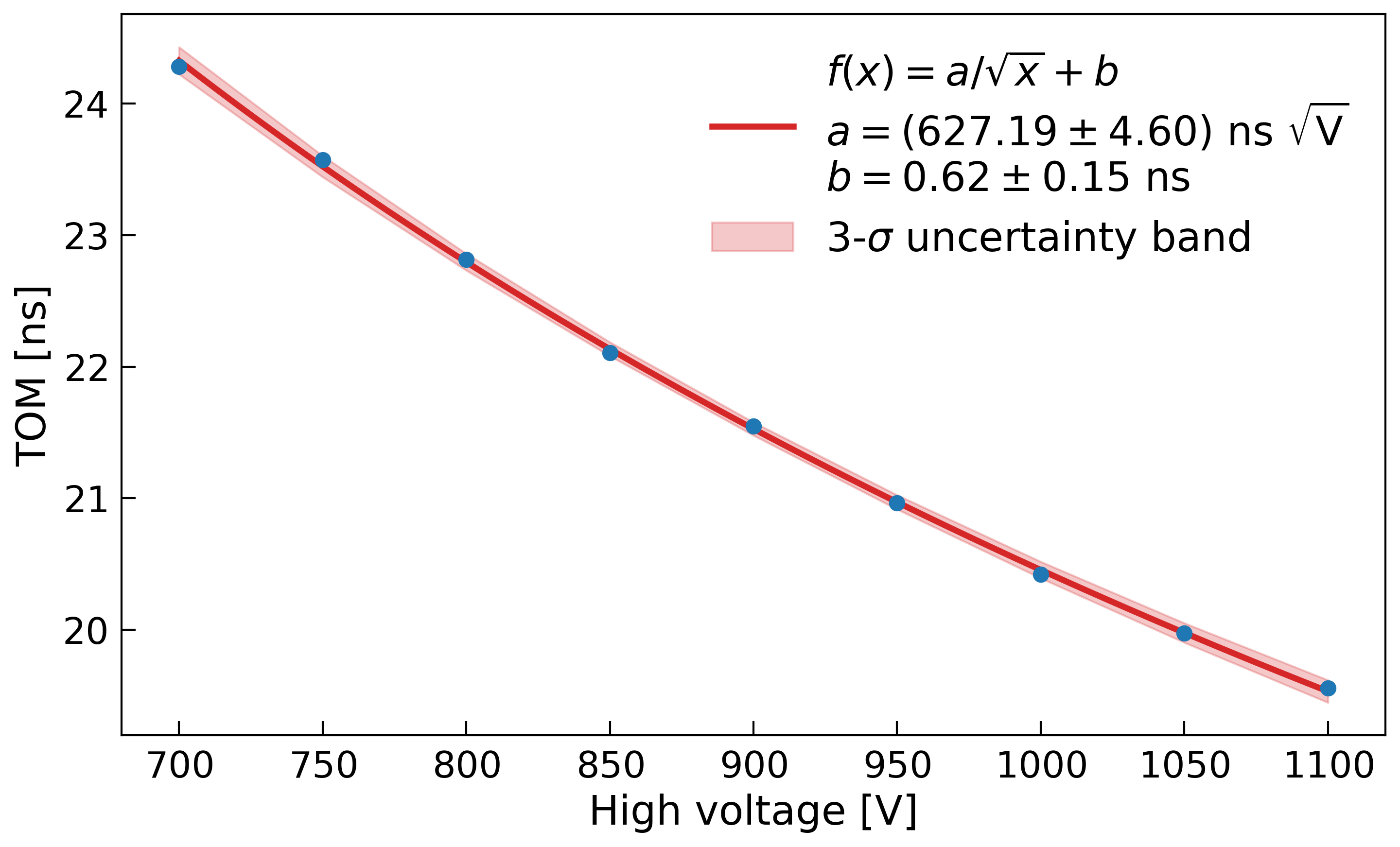
In order to correct for the PMT transit time effect, all pixels in the camera have been set to the same voltage between 700 V and 1100 V and illuminated with different intensities of the 13 LEDs of the FFCLS. For each light intensity, we have calculated the average TOM for each pixel using the scipy.signal.find_peaks method described in Section 4\xspace. A least-squares method fit has been performed for all pixels, using the function , where are the PMT voltages. This function parametrizes the time required by an electron to be accelerated by the electric field of the PMT. Figure 9\xspace shows the fit for a single pixel. The data points show the mean of the TOM over 1000 events. The results of the fit of each pixel are then used to correct for the PMT transit time effect. After calculating the fit value for each pixel at 1000 V, the TOM is shifted to the overall average of all pixel values at the same voltage. The result of the correction is shown in the right panel of Figure 8\xspace, where the mean TOM distributions of all pixels are now synchronized. The quality of the PMT transit time correction is shown by the RMS of the distribution the mean TOM for all pixels which is reduced from 0.62 ns before correction to 0.40 ns after correction. For each pixel, the fit parameters and the PMT transit time correction with respect to the average value at 1000 V are saved in a database, which will be used in the future for the calibration of the camera. In this way, if the nominal voltage of each pixel changes, we will be able to recalibrate the pixel timing to correct for the PMT transit time effect. In fact, the correction of the PMT transit time effect will take place offline, by shifting the measured TOM for each pixel to the corrected one using the aforementioned fit parameters. Due to PMT aging, the high voltage of each PMT will be adjusted to the nominal gain. Therefore, the PMT transit time is expected to change during operation time.
7 Global camera timing precision
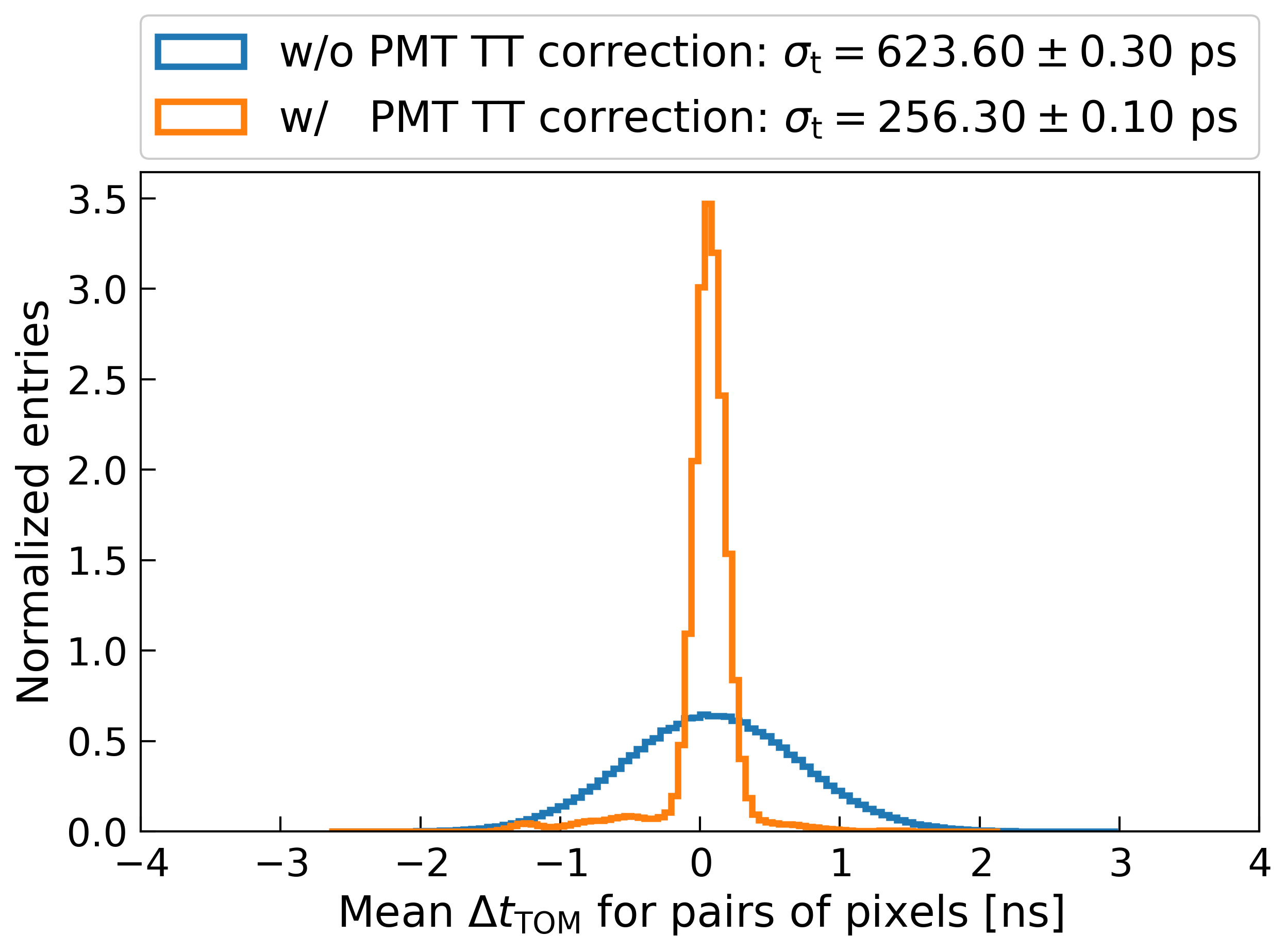
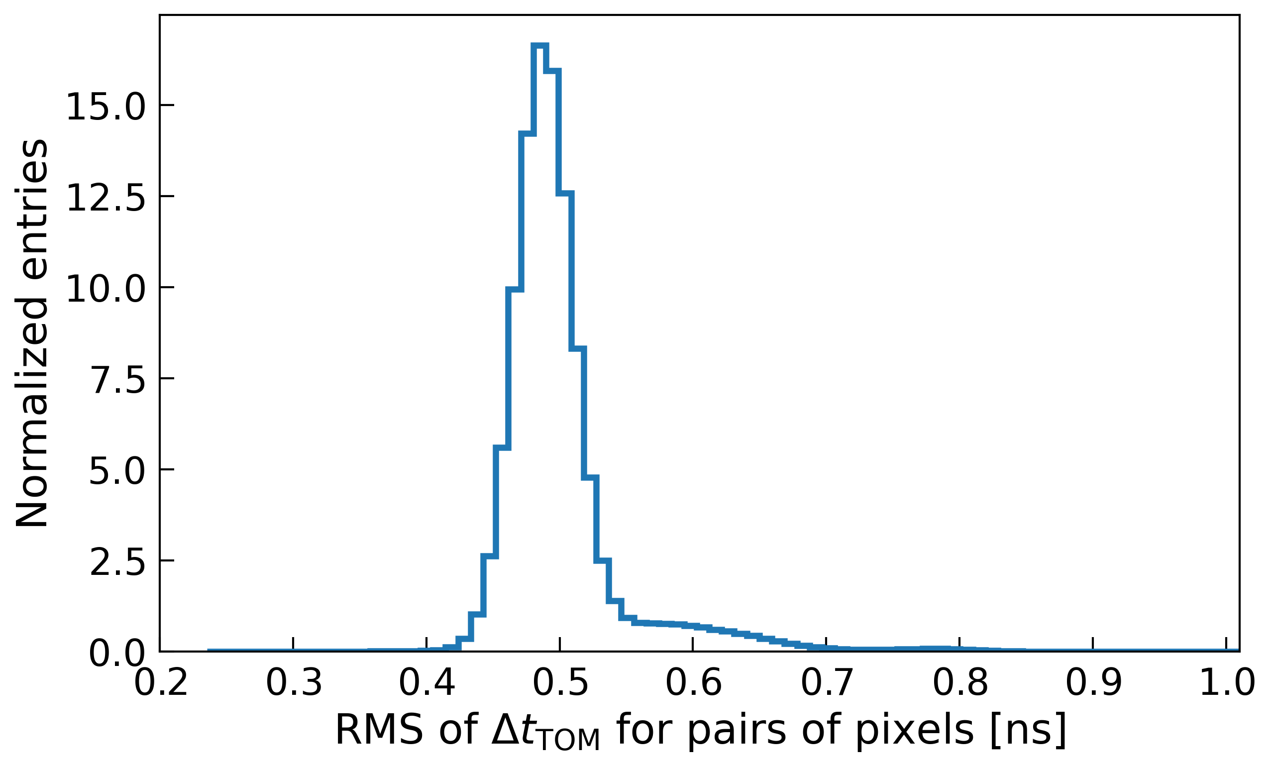
After correcting for the PMT transit time, the timing resolution of the camera can be evaluated. This measurement is performed by illuminating the camera with a uniform light at p.e. generated by the laser source. Since the measurement is performed in internal trigger mode888The internal trigger mode is the standard trigger for cosmic data taking., the calculation already takes into account the difference in distances travelled by the light before reaching any two pixels pair in the whole camera, no matter the position of the pixels in the camera. This is because the laser light source which has travel time differences between pixels is also used to perform the L1A calibration. Therefore, no geometrical correction is needed. The TOM difference between all pairs of pixels is then calculated with and without PMT transit time correction. The difference is calculated for each pair of pixels and for all events in the dataset. The final mean distribution over all events for each pair of pixels is plotted in Figure 10\xspace, with and without PMT transit time correction. After calibration, the mean of the TOM difference distribution for any two simultaneously illuminated pixels is reduced from ps to ps. Moreover, the RMS distribution of the for pair of pixels can as be computed, as shown in Figure 11\xspace. This distribution is below the 2 ns CTA requirement on the global camera timing precision.
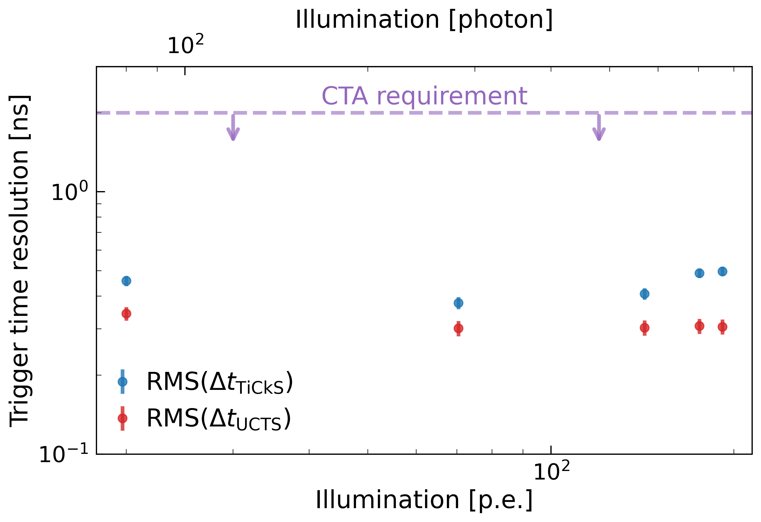
8 Camera trigger timing accuracy
The camera events are timestamped in the TiCkS board of the UCTS module. The timestamp will then be used by the CTA central trigger process to correlate the triggers of the different telescopes of the CTA array. The trigger time is required to be measured with a 2 ns accuracy.
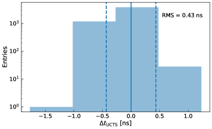
To quantify the RMS of the timestamp distribution, we have illuminated the full camera using the laser source at 1 kHz with different intensities ranging from p.e. up to p.e. For each measurement, the start time of the laser flashes are recorded with an external TiCkS board. In this way, it is possible to measure directly the time difference between the light arrival in the detection plane and the output of the timestamp to the CTA central trigger (). This method has been compared with the distribution of the time difference of two consecutive events, which gives an upper limit on the accuracy of the timestamps for a perfectly periodic input signal. Given the 1kHz frequency, the time difference between two consecutive camera trigger events is expected to be ns, as shown in Figure 12\xspace. The pixel charge for every trigger is analyzed in order to filter out the cosmic rays events, producing a histogram from which the RMS uncertainty is obtained. Figure 13\xspace shows the RMS values for every configuration used. The resulting trigger timing accuracy is better than 0.5 ns with both methods, and thus below the CTA requirements of 2 ns.
9 Conclusions
The first unit of NectarCAM has been integrated at the integration and test facility of CEA Paris-Saclay. The first timing performance verifications have shown that the camera fulfills the CTA requirements. For the test, two pulsed light sources have been used prior to calibration: a flat-field calibration light source and a laser. The single pixel timing precision has been measured to be less than 1 ns for an incoming light of intensity between and photons, making it suitable for CTA usage. The global camera timing precision has also been studied by analyzing the difference in pulse-time reconstruction between pairs of pixels. After correcting for the PMT transit time of each pixel, the time precision of the camera is reduced to 0.5 ns (Figure 11\xspace), in line with the CTA demand. Furthermore, the trigger performance has been tested. The timing accuracy that comes from the trigger timestamp of the camera relative to the time of arrival of light at the detection plane has been measured to be below 0.5 ns for the illumination range between p.e. and p.e., using two different methods. Therefore, it complies with the CTA requirements.
10 Acknowledgements
We thank the anonymous referees for carefully reading the manuscript and providing helpful suggestions that improved the clarity of the text. This work was conducted in the context of the CTA Consortium. We gratefully acknowledge financial support from the following agencies and organizations: Ministry of Higher Education and Research, CNRS-INSU and CNRS-IN2P3, CEA-Irfu, ANR, Regional Council Ile de France, Labex ENIGMASS, OCEVU, OSUG2020 and P2IO, France; DESY, Helmholtz Association, Germany; Spanish Research State Agency (AEI) through the grant PID2019-104114RB-C32.
References
- [1] A. U. Abeysekara, et al., Observation of the Crab Nebula with the HAWC Gamma-Ray Observatory, Astrophys. J. 843 (1) (2017) 39. arXiv:1701.01778, doi:10.3847/1538-4357/aa7555.
- [2] F. Aharonian, et al., The observation of the Crab Nebula with LHAASO-KM2A for the performance study, Chin. Phys. C 45 (2) (2021) 025002. arXiv:2010.06205, doi:10.1088/1674-1137/abd01b.
- [3] B. Acharya, et al., Introducing the CTA concept, Astroparticle Physics 43 (2013) 3–18, Seeing the High-Energy Universe with the Cherenkov Telescope Array - The Science Explored with the CTA. doi:https://doi.org/10.1016/j.astropartphys.2013.01.007.
- [4] K. Bernlöhr, et al., Monte Carlo design studies for the Cherenkov Telescope Array, Astroparticle Physics 43 (2013) 171–188, Seeing the High-Energy Universe with the Cherenkov Telescope Array - The Science Explored with the CTA. doi:https://doi.org/10.1016/j.astropartphys.2012.10.002.
- [5] J.-F. Glicenstein, NectarCAM : a camera for the medium size telescopes of the Cherenkov Telescope Array, PoS ICRC2015 (2016) 937. doi:10.22323/1.236.0937.
- [6] A. Tsiahina, et al., Measurement of performance of the NectarCAM photodetectors, Nuclear Instruments and Methods in Physics Research A 1007 (2021) 165413. doi:10.1016/j.nima.2021.165413.
- [7] F. Hénault, et al., Design of light concentrators for Cherenkov telescope observatories, in: R. Winston, J. Gordon (Eds.), Nonimaging Optics: Efficient Design for Illumination and Solar Concentration X, Vol. 8834 of Society of Photo-Optical Instrumentation Engineers (SPIE) Conference Series, 2013, p. 883405. doi:10.1117/12.2024049.
- [8] D. Gascon, et al., Wideband pulse amplifier with 8 GHz GBW product in a 0.35 m CMOS technology for the integrated camera of the Cherenkov Telescope Array, Journal of Instrumentation 5 (12) (2010) C12034. doi:10.1088/1748-0221/5/12/C12034.
- [9] E. Delagnes, et al., NECTAr0, a new high speed digitizer ASIC for the Cherenkov Telescope Array, in: 2011 IEEE Nuclear Science Symposium Conference Record, 2011, pp. 1457–1462. doi:10.1109/NSSMIC.2011.6154348.
- [10] U. Schwanke, et al., A versatile digital camera trigger for telescopes in the Cherenkov Telescope Array, Nuclear Instruments and Methods in Physics Research Section A: Accelerators, Spectrometers, Detectors and Associated Equipment 782 (2015) 92–103. doi:https://doi.org/10.1016/j.nima.2015.01.096.
- [11] D. Gascon, et al., Reconfigurable ASIC for a low level trigger system in Cherenkov Telescope Cameras, Journal of Instrumentation 11 (11) (2016) P11017. doi:10.1088/1748-0221/11/11/P11017.
- [12] T. Armstrong, et al., Monte Carlo Simulations and Validation of NectarCAM, a Medium Sized Telescope Camera for CTA, in: 37th International Cosmic Ray Conference, 2022, p. 747. doi:10.22323/1.395.0747.
-
[13]
J. Kapustinsky, R. DeVries, N. DiGiacomo, W. Sondheim, J. Sunier, H. Coombes,
A
fast timing light pulser for scintillation detectors, Nuclear Instruments
and Methods in Physics Research Section A: Accelerators, Spectrometers,
Detectors and Associated Equipment 241 (2) (1985) 612–613.
doi:https://doi.org/10.1016/0168-9002(85)90622-9.
URL https://www.sciencedirect.com/science/article/pii/0168900285906229 - [14] L. A. Tejedor, J. A. Barrio, P. Peñil, A. Pérez, D. Herranz, J. Martín, A trigger interface board for the large and medium sized telescopes of the cherenkov telescope array, Nuclear Instruments and Methods in Physics Research Section A: Accelerators, Spectrometers, Detectors and Associated Equipment 1027 (2022) 166058. doi:https://doi.org/10.1016/j.nima.2021.166058.
- [15] B. Biasuzzi, et al., Design and characterization of a single photoelectron calibration system for the nectarcam camera of the medium-sized telescopes of the cherenkov telescope array, Nuclear Instruments and Methods in Physics Research Section A: Accelerators, Spectrometers, Detectors and Associated Equipment 950 (2020) 162949. doi:https://doi.org/10.1016/j.nima.2019.162949.
- [16] C. Champion, et al., TiCkS: A Flexible White-Rabbit Based Time-Stamping Board, in: 16th International Conference on Accelerator and Large Experimental Physics Control Systems, 2018, p. TUPHA090. doi:10.18429/JACoW-ICALEPCS2017-TUPHA090.
- [17] M. Lipiński, et al., White rabbit: a ptp application for robust sub-nanosecond synchronization, in: 2011 IEEE International Symposium on Precision Clock Synchronization for Measurement, Control and Communication, 2011, pp. 25–30. doi:10.1109/ISPCS.2011.6070148.
- [18] Ieee standard for a precision clock synchronization protocol for networked measurement and control systems, IEEE Std 1588-2019 (Revision ofIEEE Std 1588-2008) (2020) 1–499doi:10.1109/IEEESTD.2020.9120376.
- [19] Ieee standard for test access port and boundary-scan architecture - redline, IEEE Std 1149.1-2013 (Revision of IEEE Std 1149.1-2001) - Redline (2013) 1–899.
- [20] D. Hoffmann, et al., 40 gbps data acquisition system for nectarcam, Journal of Physics: Conference Series 898 (3) (2017) 032015. doi:10.1088/1742-6596/898/3/032015.
- [21] F. Bradascio, Improved performances of the NectarCAM, a Medium-Sized Telescope Camera for the Cherenkov Telescope Array, 2022, p. 25. doi:10.58027\%2Fx1th-cw93.
- [22] P. Virtanen, et al., SciPy 1.0: fundamental algorithms for scientific computing in python, Nature Methods 17 (3) (2020) 261–272. doi:10.1038/s41592-019-0686-2.
- [23] T. Tavernier, et al., Status and performance results from NectarCAM – a camera for CTA medium sized telescopes, PoS ICRC2019 (2020) 805. doi:10.22323/1.358.0805.
- [24] W. R. Leo, Techniques for nuclear and particle physics experiments: a how-to approach; 2nd ed., Springer, Berlin, 1994. doi:10.1007/978-3-642-57920-2.
- [25] L. A. Tejedor, et al., An Analog Delay Compensation System to Reduce the Effect of Variable Transit Time in PMTs, IEEE Transactions on Nuclear Science 60 (4) (2013) 2905–2911. doi:10.1109/TNS.2013.2271300.