[a]Tamas Almos Vami
Simulated performance and calibration of CMS Phase-2 Upgrade Inner Tracker sensors
Abstract
The next upgrade of the Large Hadron Collider (LHC) is planned from 2026 when the collider will move to its High Luminosity phase (HL-LHC). The CMS detector needs to be substantially upgraded during this period to exploit the fourfold increase in luminosity provided by the HL-LHC. This upgrade is referred to as the CMS Phase-2 Upgrade. A program of laboratory and beam test measurements, and performance studies based on the detailed simulation of the detector was carried out to support the decision of the technology of the sensors to be adopted in the different regions of the detector for the Phase-2 Upgrade. Among the various options considered, CMS chose to use 3D sensors with a 25 100 m2 pixel cell in the innermost layer of the barrel and planar sensors with a 25 100 m2 pixel cell elsewhere. In this paper, we detail the simulation studies that were carried out to choose the best sensor design. These studies include a detailed standalone simulation of the sensors made with PixelAV and the expected performance on high level observables obtained with the simulation and reconstruction software of the CMS experiment.
1 Introduction
The Large Hadron Collider (LHC) will be upgraded to its High Luminosity phase (HL-LHC) in the shutdown period from 2026. The HL-LHC will reach the instantaneous luminosity of which is four times the Run-2 value of . The number of simultaneous proton-proton interactions per 25 ns bunch crossing (pileup) is expected to be between 140 and 200, which is a similar fourfold increase with respect to the current value of 55. The current detectors would not be able to operate in such conditions, which motivates the need to upgrade them. This is referred to as the Phase-2 Upgrade of CMS.
The upgraded CMS tracker detector [1] will provide increased acceptance for tracking up to and significantly reduced mass through the use of carbon fiber mechanics, and cooling. The layout of the upgraded tracker is shown in Fig. 1. It consists of two parts, the Outer Tracker (OT) and the Inner Tracker (IT). The OT has six barrel layers and five pairs of forward disks, while the IT has four barrel layers and twelve pairs of forward disks.
The IT has 3900 hybrid modules which use either two or four read out chips per module. The read out chips are designed by the RD53 collaboration [2]. Sensors are bump bonded to the readout chip in a 50 50 pattern. The active thickness of the sensors is 150 m for all the scenarios considered. This paper details the sensors properties used in the IT, such as the pixel dimensions and technologies used.
2 PixelAV simulation description
PixelAV simulations use a charge deposition model based on the Bichsel pion-Si cross sections [5]. The delta-ray range is calculated using the continuously slowing-down approach with NIST ESTAR dE/dx data [6]. The carrier transport on a given charge (q) is based on the Runge-Kutta integration of the saturated drift velocity (v). The velocity is calculated as shown in Equation 1 for a given electric (E) and magnetic (B) field, where is the mobility and is the Hall factor.
| (1) |
The electric field is derived from an ISE TCAD simulation of a pixel cell. The TCAD simulations include effects for charge trapping, diffusion, and induction on implants. After this, there is an electronics simulation, where we apply noise, linearity, thresholds, and miscalibration effects.
Irradiation simulations for the Phase-2 sensors are based on models developed for the 2018 Phase-1 detector (based on data corresponding to a fluence of ), but are scaled to the fluence expected from the HL-LHC. The read-out chip threshold is 1000 electrons for all cases discussed below.
Cross talk with neighboring pixels depends on the geometry; pixel size of 25 100 generates 10% crosstalk, while the 50 50 generates no crosstalk. The bias voltage assumptions for the 25 100 sensors start with 350 V, and for 50 50 start with 100 V. In both cases, the bias voltage (HV) is increased to to maximize the signal efficiency.
Simulations are evaluated by comparing detector resolution as a function of track angle (). We use the same calibrations and reconstruction algorithm as used in CMSSW. Resolution is obtained by taking the RMS of the residual distribution between measured and expected hit positions, which better accounts for non-Gaussian tails. These measurements are performed in two charge bins: 0 < < 1 and 1 < < 1.5, where is the charge and is the average charge produced by the hit.
Another important parameter is the charge collection efficiency (CCE) which is defined as the ratio of collected charge to all charge generated.
3 Pixel size studies
In this section, we compare the pixel size options of 50 50 and 25 100 . Figure 2 shows the resolution (RMS) as a function of the track angle for unirradiated sensors in both the coordinate (along the beam), and the coordinate (azimuthal angle). Red lines correspond to the 50 50 choice, while the blue lines correspond to the 25 100 choice. The CCE for the unirradiated case is 100%.
We observe that the 50 50 performs better in the beam direction, while the 25 100 performs better in the azimuth direction. The local maxima of the curve is at boundaries when transitioning from a single pixel cluster to a double pixel cluster, or higher cluster sizes.
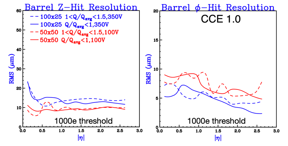
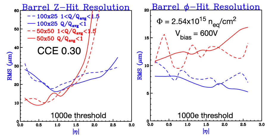
Figure 3 shows the resolutions but for irradiated sensors after 3000 fb-1, which corresponds to the end of HL-LHC running and a fluence of . In this case the bias voltage is increased to 600 V to maximise the signal efficiency.
The situation is very different from the unirradiated case. Now the 50 50 case only performs better in the low regions, but breaks down at high . On the other hand, the 25 100 still performs better in the azimuth direction. Based on these results the 25 100 is the better choice in terms of the pixel dimensions.
4 Sensor technology studies
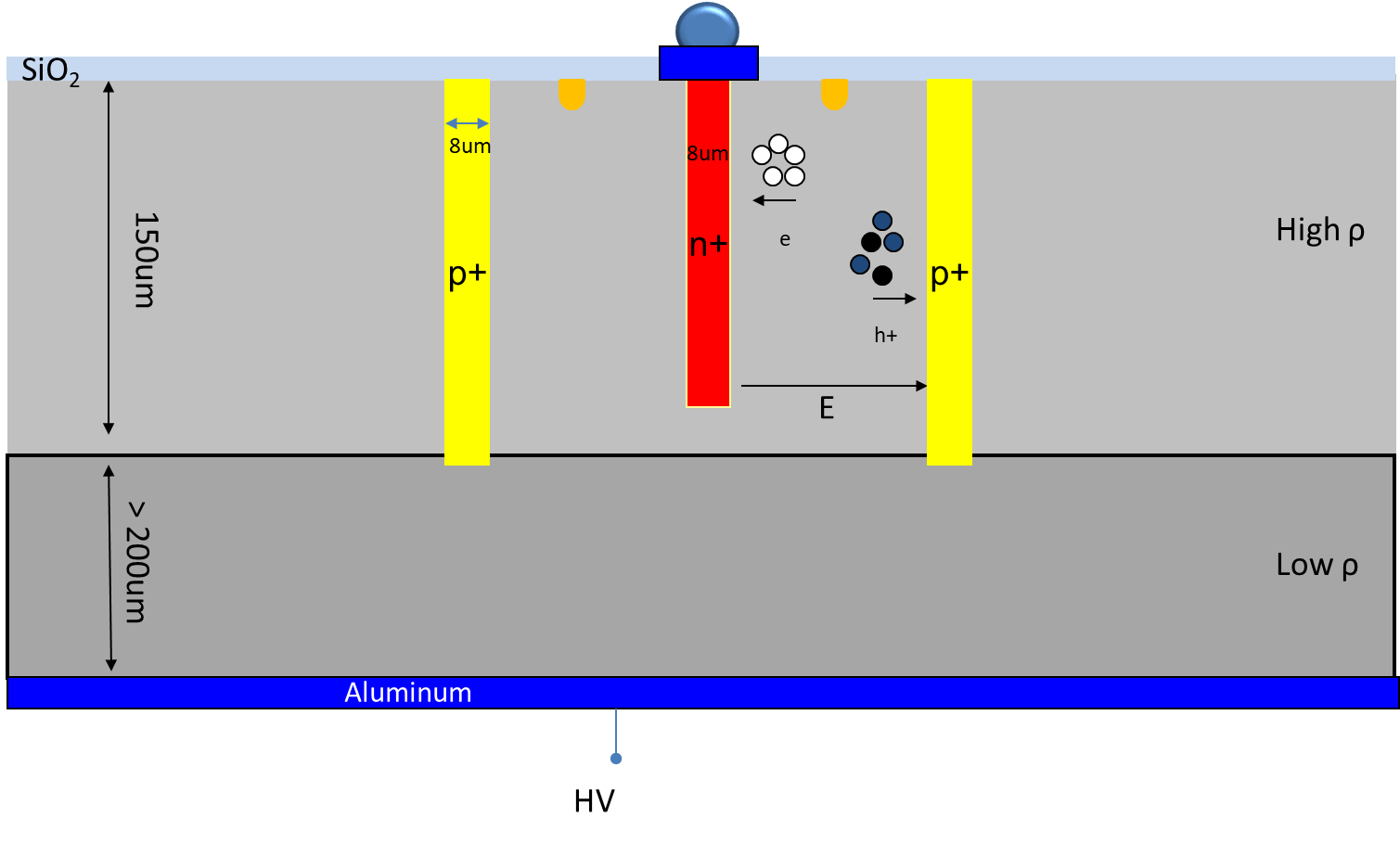
Besides planar sensors, the possibility of 3D sensors was considered. Figure 4 shows how 3D sensors differ from planar sensors by collecting charge on columnar implants that penetrate the substrate.
The original version of PixelAV used a segmented parallel plate capacitor model to estimate the signal induced by trapped carriers. While this works well for planar sensors, it cannot be used to describe more complex, less symmetric implant geometries. PixelAV was therefore modified to use a lookup table based implementation of the Ramo-Shockley weighting potential. This is a general method that works for 3D sensors as well.
The potential function is the solution of Laplace’s equation for a system of electrodes with , , and for as shown in Fig. 5.
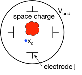
Charge on electrode () induced by carrier at is
| (2) |
where the is the weighting potential and is the charge of the carrier.
One further complication for 3D sensors is that TCAD 9.0 does not support meshing across region boundaries to calculate the weighting potential. To resolve this, we place equipotential conducting "contacts" on the inside surfaces of square voids to represent the implants in a 2.5 x 2.5 pixel array.
After these modifications, the electric field maps generated by TCAD for the 3D sensors can be seen in Fig. 6.
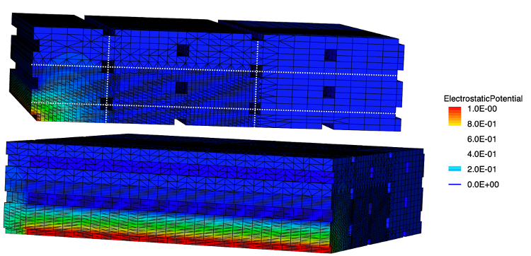
Figure 7 shows the residuals as a function of the track angle for the 3D sensor case for three irradiation scenarios; dark blue corresponds to new sensors operated at 40 V, turquoise corresponds to sensors operated at 75 V, after 370 fb-1 irradiation, and magenta is for 150 V with irradiation after 2000 fb-1.
We can observe that the 3D sensors after 370 fb-1 perform similarly to unirradiated sensors, while at 2000 fb-1 the resolutions show the effect of charge loss. The CCE is reduced to 84% for irradiation after 370 fb-1 and to 32% for irradiation after 2000 fb-1.
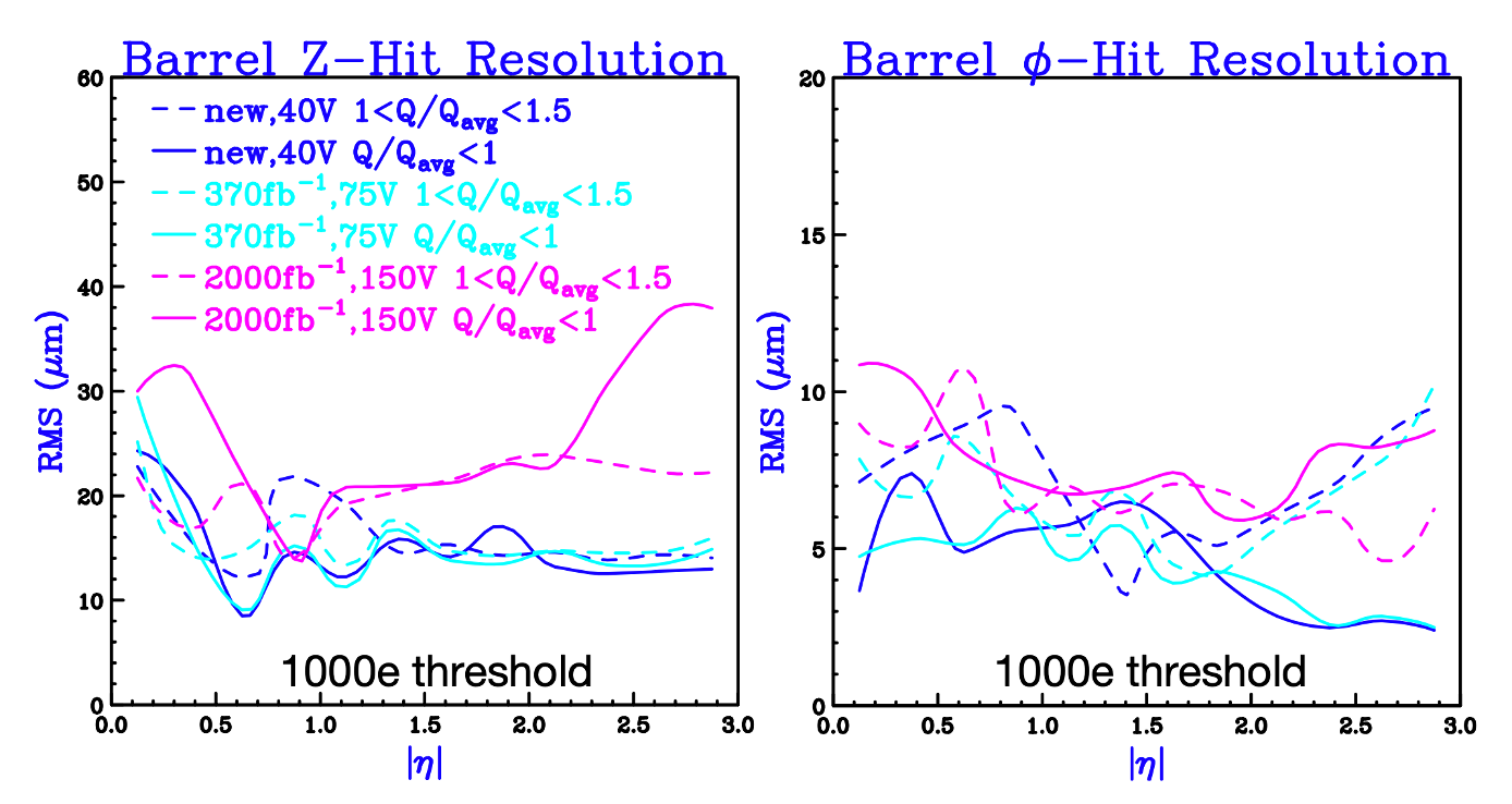
Table 1 shows the summary of different irradiation scenarios for the 3D sensors and their performance. The sensors after irradiation at 2000 fb-1 need 150 V bias voltage (HV) setting, otherwise significant cluster breakage is observed. Resolutions in the beam and azimuth directions are averaged over all pseudorapidity.
| Scenario | New | 370 fb-1 | 2000 fb-1 |
|---|---|---|---|
| Fluence | 0 | ||
| Bias | 40 V | 75 V | 150 V |
| Resolution (Z) | 13.9 m | 14.3 m | 22.5 m |
| Resolution () | 5.6 m | 5.9 m | 9.8 m |
| CCE | 0.96 | 0.84 | 0.39 |
In summary, 3D sensors have excellent performance after irradiation with resolutions comparable to current detector performance. Based on these plots 3D sensors are a better choice for the first layer of the IT.
5 Simulation of avalanche gain effect
The avalanche gain effect is non-negligible for high bias voltage values for the Phase-2 planar sensors. This section details how to include this effect in the PixelAV simulations using test beam data from DESY. The test beam data corresponds to an irradiation of (denoted as "Data 40x") and contains several bias voltage settings. We studied the charge profiles, i.e. the path length normalized pixel charge as a function of the sensor depth, using each setting. We observe that lower bias voltage settings (less than 600 V) are better described by the simulations, while for the higher bias voltage settings, the peak charge and the total charge both deviate from the predictions of the simulation.
In order to improve on this, PixelAV was updated to include a gain factor when collecting electrons. We performed a scan for each sample with a gain factor variation and selected the gain factor that describes the charge profile of the data the best. Figure 8 shows the selected gain factors as a function of the peak electric field extracted from TCAD. The uncertainty of the gain factor value is estimated to be 0.01. Reference [7] suggests the function g(E):
| (3) |
where is the coefficient of the impact ionization for electrons/holes, and is the parameter for the breakdown electric field.
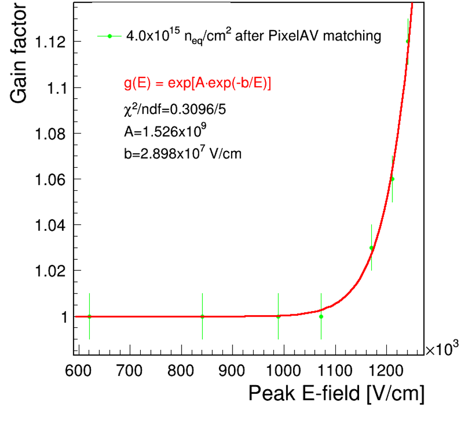
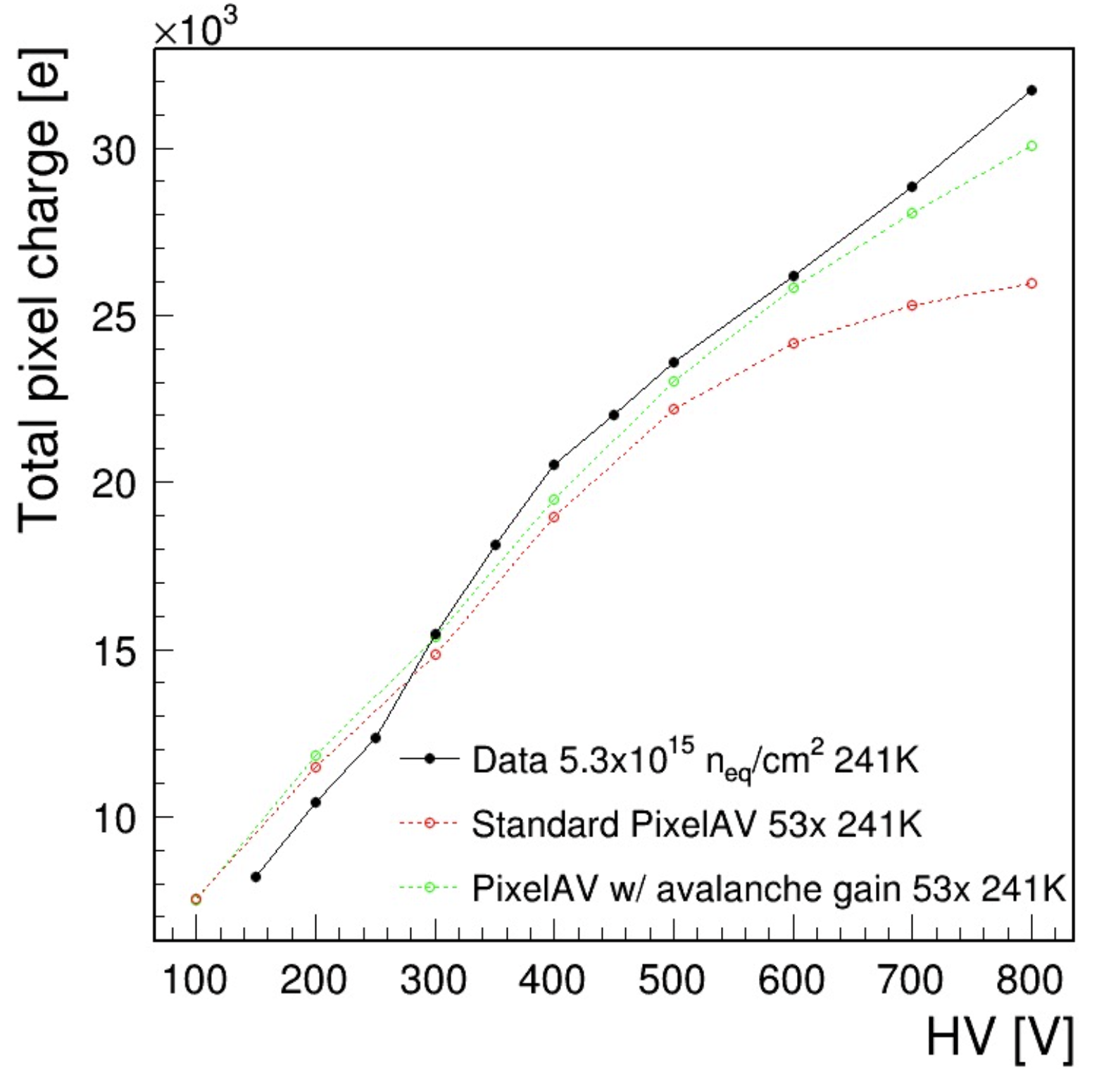
To validate this procedure, we used test beam data with sensors irradiated at and compared against simulations in which we included the avalanche gain effect with the parameterization from the data studies. The results are shown in Fig. 8. Black points correspond to the test beam data, the red points are the standard PixelAV simulation and the green points are PixelAV with the avalanche gain effect. For the PixelAV simulations (red and green) we rescaled the fluences to .
The charges in the simulation without avalanche gain effect deviate from the data at higher bias voltages, while the simulation including avalanche gain effect is better at describing the test beam data.
6 CMSSW full simulations
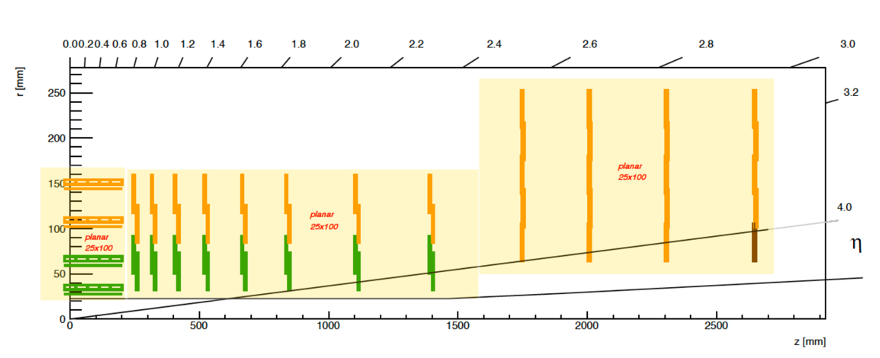
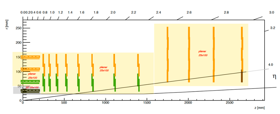
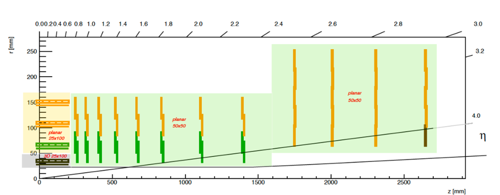
This section compares the scenarios detailed in the above sections using CMSSW. It should be noted that there is no radiation simulation yet in CMSSW, so all these results correspond to unirradiated sensors. Physics performance was evaluated for three layouts of the IT, which are shown in Fig. 9. These layouts sketch a quarter of the Inner Tracker in the r-z view generated using the tkLayout tool [8]. Modules with 1x2 readout chips are shown in green, modules with 2x2 readout chips are shown in orange. The three layouts are defined as:
-
•
T21: 25 100 in the both the barrel and the endcaps.
-
•
T25: 25 100 in the both the barrel and the endcaps, but 3D sensors in the first barrel layer.
-
•
T26: 25 100 in the barrel, with 3D sensors in the first barrel layer, and 50 50 planar sensors the endcaps.
We used two different samples of 80 000 simulated events at :
-
•
Single-track (muon) events for tracking performance studies, consisting of a flat spectrum of [1, 200] GeV, without smearing of the primary vertex.
-
•
events with pileup of 200 for heavy flavor tagging studies, generated with an approximately 4 cm Gaussian smearing of the beamspot along the beamline.
In terms of tracking performance, the resolution on the track impact parameter as a function of track angle is shown in Fig. 10. Blue points correspond to the T21 geometry, green to the T25 geometry and the red to the T26 geometry. Resolution is computed for tracks which have at least one-hit in the IT. The result from T21 layout is used as the reference (denominator) in the ratio plots.
The comparison of 25 100 planar (T21) and 25 100 3D sensors (T25 and T26) for barrel-only tracks, , shows that the resolution on track impact parameter, both in the transverse dimension () and the longitudinal dimension (), is the same when the first barrel layer is built with planar or 3D sensors. Comparison for endcap-only tracks, , shows that the improvement of the resolution in one projection is approximately of the same amount as the deterioration in the other.
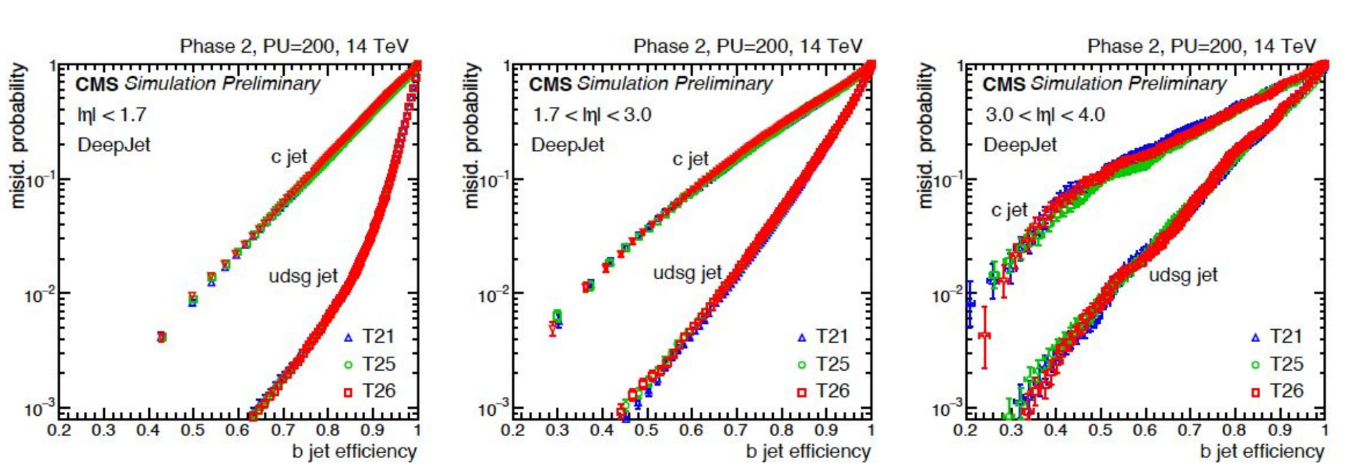
Heavy flavor tagging performance is shown in Fig. 11, where ROC curves describe light-/charm-jet contamination as a function of b-jet efficiency for the “DeepJet” tagger [9] in three regions of : , , . The edges of the bins were defined to minimize migration effects. The corresponding number of jets per bin is 360k , 105k and 15k, respectively.
.
For central jets (|| < 3.0), Fig. 11 shows that there is no difference in performance between the three geometries. This result is expected as the simulated impact parameter resolution for single muons is identical for each layout. For forward jets (|| > 3.0) however, the performance differential between T26 and T21/T25 geometries is minor and suggests that pixel sizes of 25 100 could be used throughout the Inner Tracker.
These finding are in line with the simulations of the irradiated sensors discussed in the earlier chapters. With all these considerations, the final design choice is T25, i.e. 3D sensors in the first layer, and planar sensors everywhere else, with a pixel size of 25 100 .
7 Conclusions
In this paper, the HL-LHC and CMS Phase-2 Inner Tracker project was introduced. PixelAV, TCAD simulations were detailed, especially concentrating on how they are used to simulate irradiated sensors. Different pixel sizes (50 50 and 25x100 ) and sensor technologies (planar and 3D sensors) were studied. The development in PixelAV to simulate 3D sensors using the Ramo–Shockley theorem and weighting potentials was presented. Simulations to DESY test beam data were compared and the avalanche gain effect for planar sensors was characterized. The tracking and heavy flavor tagging performance of three layouts in CMSSW were studied. Following these and other studies, the decision has been made to use 3D sensors in the first layer of the barrel, and use planar sensors in everywhere else. The decision for the size of the pixels is to use 25x100 .
References
- [1] CMS Collaboration, The Phase-2 Upgrade of the CMS Tracker, CERN-LHCC-2017-009, CMS-TDR-014 (2017) .
- [2] J.C. Chistiansen and M.L. Garcia-Sciveres, RD Collaboration Proposal: Development of pixel readout integrated circuits for extreme rate and radiation, CERN-LHCC-2013-008, LHCC-P-006 (2013) .
- [3] CMS Collaboration, Technical design report volume 1: Detector performance and software, CERN-LHCC-2006-001, CMS-TDR-8-1 (2006) .
- [4] V. Chiochia et al., Simulation of the CMS prototype silicon pixel sensors and comparison with test beam measurements, IEEE Trans. Nucl. Sci. 52 (2005) 1067.
- [5] H. Bichsel, Straggling in thin silicon detectors, Rev. Mod. Phys. 60 (1988) 663.
- [6] M. Berger, J. Coursey and M. Zucker, ESTAR, PSTAR, and ASTAR: Computer programs for calculating stopping-power and range tables for electrons, protons, and helium ions, NIST (1992) .
- [7] Y. Serezhkin and A. Shesterkina, Carrier multiplication in silicon p-n junctions, Semiconductors 37 (2003) 1085.
- [8] S. Mersi, D. Abbaneo, N. de Maio and G. Hall, Software package for the characterization of tracker layouts, Astroparticle, Particle, Space Physics, Radiation Interaction, Detectors and Medical Physics Applications 7 (2012) 1015.
- [9] E. Bols, J. Kieseler, M. Verzetti, M. Stoye and A. Stakia, Jet flavour classification using DeepJet, Journal of Instrumentation 15 (2020) P12012.